 | –≠–ª–µ–∫—Ç—Ä–æ–Ω–Ω—ã–π –∫–æ–º–ø–æ–Ω–µ–Ω—Ç: STPS3045C | –°–∫–∞—á–∞—Ç—å:  PDF PDF  ZIP ZIP |
1/9
STPS3045CT/CG/CR/CP/CPI/CW/CFP
Æ
July 2003 - Ed: 6E
POWER SCHOTTKY RECTIFIER
I
F(AV)
2 x 15 A
V
RRM
45 V
T
j
(max)
175 ∞C
V
F
0.57 V
MAIN PRODUCT CHARACTERISTICS
s
VERY SMALL CONDUCTION LOSSES
s
NEGLIGIBLE SWITCHING LOSSES
s
EXTREMELY FAST SWITCHING
s
LOW THERMAL RESISTANCE
s
INSULATED PACKAGE: TOP-3I
Insulating voltage = 2500V RMS
Capacitance = 12pF
s
AVALANCHE CAPABILITY SPECIFIED
FEATURES AND BENEFITS
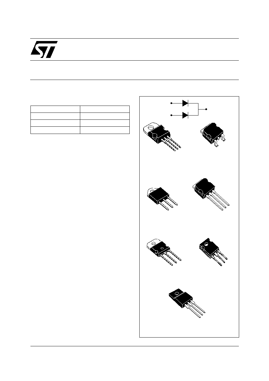
Dual center tap Schottky rectifier suited for
SwitchMode Power Supply and high frequency DC
to DC converters.
Packaged either in TO-220AB, TO-220FPAB,
D
2
PAK, I
2
PAK, TO-247, SOT93 or TOP-3I, this
device is especially intended for use in low volt-
age, high frequency inverters, free wheeling and
polarity protection applications.
DESCRIPTION
D
2
PAK
STPS3045CG
A2
A1
K
A1
A2
K
TO-220AB
STPS3045CT
A1
A2
K
SOT-93
STPS3045CP
Insulated
TOP-3I
STPS3045CPI
TO-220FPAB
STPS3045CFP
K
A1
A2
K
A1
A2
A1
K
A2
A1
A2
K
I
2
PAK
STPS3045CR
A1
K
A2
TO-247
STPS3045CW

STPS3045CT/CG/CR/CP/CPI/CW/CFP
2/9
Symbol
Parameter
Value
Unit
R
th(j-c)
Junction to case
TO-220AB / D
2
PAK / I
2
PAK
Per diode
Total
1.60
0.85
∞C/W
SOT-93 / TO-247
Per diode
Total
1.5
0.8
TO-220FPAB
Per diode
Total
4
3.2
TOP-3I
Per diode
Total
2.2
1.6
R
th(c)
TO-220AB / D
2
PAK / I
2
PAK
SOT-93 / TO-247
Coupling
0.10
TO-220FPAB
Coupling
2.5
TOP-3I
Coupling
1.0
When the diodes 1 and 2 are used simultaneously:
Tj (diode 1) = P (diode1) x R
th(j-c)
(per diode) + P (diode 2) x R
th(c)
THERMAL RESISTANCES
Symbol
Parameter
Value
Unit
V
RRM
Repetitive peak reverse voltage
45
V
I
F(RMS)
RMS forward current
30
A
I
F(AV)
Average forward
current
= 0.5
TO-220AB / D
2
PAK /
I
2
PAK / SOT-93 / TO-247
Tc = 155∞C
Per diode
Per de-
vice
15
30
A
TO-220FPAB
Tc = 130∞C
TOP-3I
Tc = 150∞C
I
FSM
Surge non repetitive forward current
t
p
= 10 ms sinusoidal
220
A
I
RRM
Repetitive peak reverse current
t
p
= 2 µs square
F = 1kHz
1
A
I
RSM
Non repetitive peak reverse current
tp = 100 µs square
3
A
P
ARM
Repetitive peak avalanche power
tp = 1µs
Tj = 25∞C
6000
W
T
stg
Storage temperature range
-65 to +175
∞C
T
j
Maximum operating junction temperature *
175
∞C
dV/dt
Critical rate of rise of reverse voltage
10000
V/µs
ABSOLUTE RATINGS (limiting values, per diode)
* :
dPtot
dTj
Rth j
a
<
-
1
(
)
thermal runaway condition for a diode on its own heatsink
Symbol
Parameter
Tests Conditions
Min.
Typ.
Max.
Unit
I
R
*
Reverse leakage current
Tj = 25∞C
V
R
= V
RRM
200
µA
Tj = 125∞C
11
40
mA
V
F
*
Forward voltage drop
Tj = 125
∞
C
I
F
= 15 A
0.5
0.57
V
Tj = 25
∞
C
I
F
= 30 A
0.84
Tj = 125∞C
I
F
= 30 A
0.65
0.72
STATIC ELECTRICAL CHARACTERISTICS (Per diode)
Pulse test :
* tp = 380 µs,
< 2%
To evaluate the conduction losses use the following equation :
P = 0.42 x I
F(AV)
+ 0.01 I
F
2
(RMS)
STPS3045CT/CG/CR/CP/CPI/CW/CFP
3/9
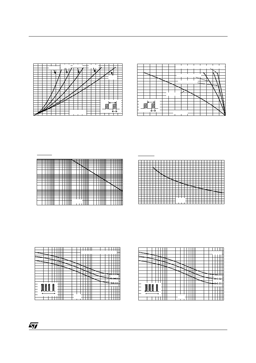
P
(W)
F(AV)
0
1
2
3
4
5
6
7
8
9
10
11
12
0
2
4
6
8
10
12
14
16
18
20
= 0.05
= 0.1
= 0.2
= 0.5
= 1
I
(A)
F(AV)
T
=tp/T
tp
Fig. 1: Average forward power dissipation versus
average forward current (per diode).
I
(A)
F(AV)
0
2
4
6
8
10
12
14
16
18
0
25
50
75
100
125
150
175
T
(∞C)
amb
T
=tp/T
tp
R
=15∞C/W
th(j-a)
R
=R
(TO-220FPAB)
th(j-a)
th(j-c)
R
=R
(TOP-3I)
th(j-a)
th(j-c)
R
=R
(TO-220AB, I PAK, D PAK, SOT-93, TO-247)
th(j-a)
th(j-c)
2
2
Fig.
2:
Average
current
versus
ambient
temperature (
= 0.5, per diode).
I (A)
M
0
20
40
60
80
100
120
140
160
180
200
1.E-03
1.E-02
1.E-01
1.E+00
I
M
t
=0.5
t(s)
TO-220AB, I2PAK, D PAK, SOT-93, TO-247
2
T =75∞C
C
T =100∞C
C
T =125∞C
C
Fig. 5-1: Non repetitive surge peak forward current
versus overload duration (maximum values, per
diode).
0
20
40
60
80
100
120
140
160
1.E-03
1.E-02
1.E-01
1.E+00
I (A)
M
I
M
t
=0.5
t(s)
TOP-3I
T =75∞C
C
T =100∞C
C
T =125∞C
C
Fig. 5-2: Non repetitive surge peak forward current
versus overload duration (maximum values, per
diode).
0
0.2
0.4
0.6
0.8
1
1.2
0
25
50
75
100
125
150
T (∞C)
j
P
(t )
P
(25∞C)
ARM p
ARM
Fig. 4: Normalized avalanche power derating
versus junction temperature.
0.001
0.01
0.1
0.01
1
0.1
10
100
1000
1
t (µs)
p
P
(t )
P
(1µs)
ARM p
ARM
Fig. 3: Normalized avalanche power derating
versus pulse duration.
STPS3045CT/CG/CR/CP/CPI/CW/CFP
4/9
0
20
40
60
80
100
120
1.E-03
1.E-02
1.E-01
1.E+00
I (A)
M
I
M
t
=0.5
t(s)
TO-220FPAB
T =75∞C
C
T =100∞C
C
T =125∞C
C
Fig. 5-3: Non repetitive surge peak forward current
versus overload duration (maximum values, per
diode).
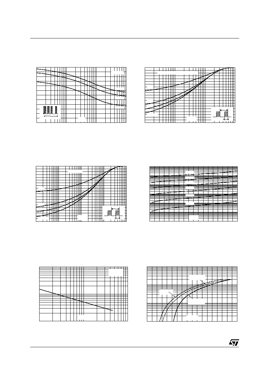
Z
/R
th(j-c)
th(j-c)
0.0
0.1
0.2
0.3
0.4
0.5
0.6
0.7
0.8
0.9
1.0
1.E-03
1.E-02
1.E-01
1.E+00
1.E+01
t (s)
p
T
=tp/T
tp
= 0.5
= 0.2
= 0.1
Single pulse
TO-220FPAB
Fig. 6-2: Relative variation of thermal transient
impedance junction to case versus pulse duration.
1.E-01
1.E+00
1.E+01
1.E+02
1.E+03
1.E+04
1.E+05
0
5
10
15
20
25
30
35
40
45
I (µA)
R
V (V)
R
T =150∞C
j
T =125∞C
j
T =100∞C
j
T =75∞C
j
T =50∞C
j
T =25∞C
j
Fig. 7: Reverse leakage current versus reverse
voltage applied (typical values, per diode).
C(nF)
100
1000
10000
1
10
100
V (V)
R
F=1MHz
V
=30mV
T =25∞C
OSC
RMS
j
Fig. 8: Junction capacitance versus reverse
voltage applied (typical values, per diode).
I
(A)
FM
1
10
100
1000
0.0
0.2
0.4
0.6
0.8
1.0
1.2
1.4
1.6
1.8
V
(V)
FM
T =125∞C
(maximum values)
j
T =125∞C
(typical values)
j
T =25∞C
(maximum values)
j
Fig. 9: Forward voltage drop versus forward
current (maximum values, per diode).
Z
/R
th(j-c)
th(j-c)
0.0
0.1
0.2
0.3
0.4
0.5
0.6
0.7
0.8
0.9
1.0
1.E-03
1.E-02
1.E-01
1.E+00
t (s)
p
T
=tp/T
tp
= 0.5
= 0.2
= 0.1
Single pulse
TO-220AB, I PAK, D PAK, SOT-93, TOP-3I, TO-247
2
2
Fig. 6-1: Relative variation of thermal transient
impedance junction to case versus pulse duration.
STPS3045CT/CG/CR/CP/CPI/CW/CFP
5/9
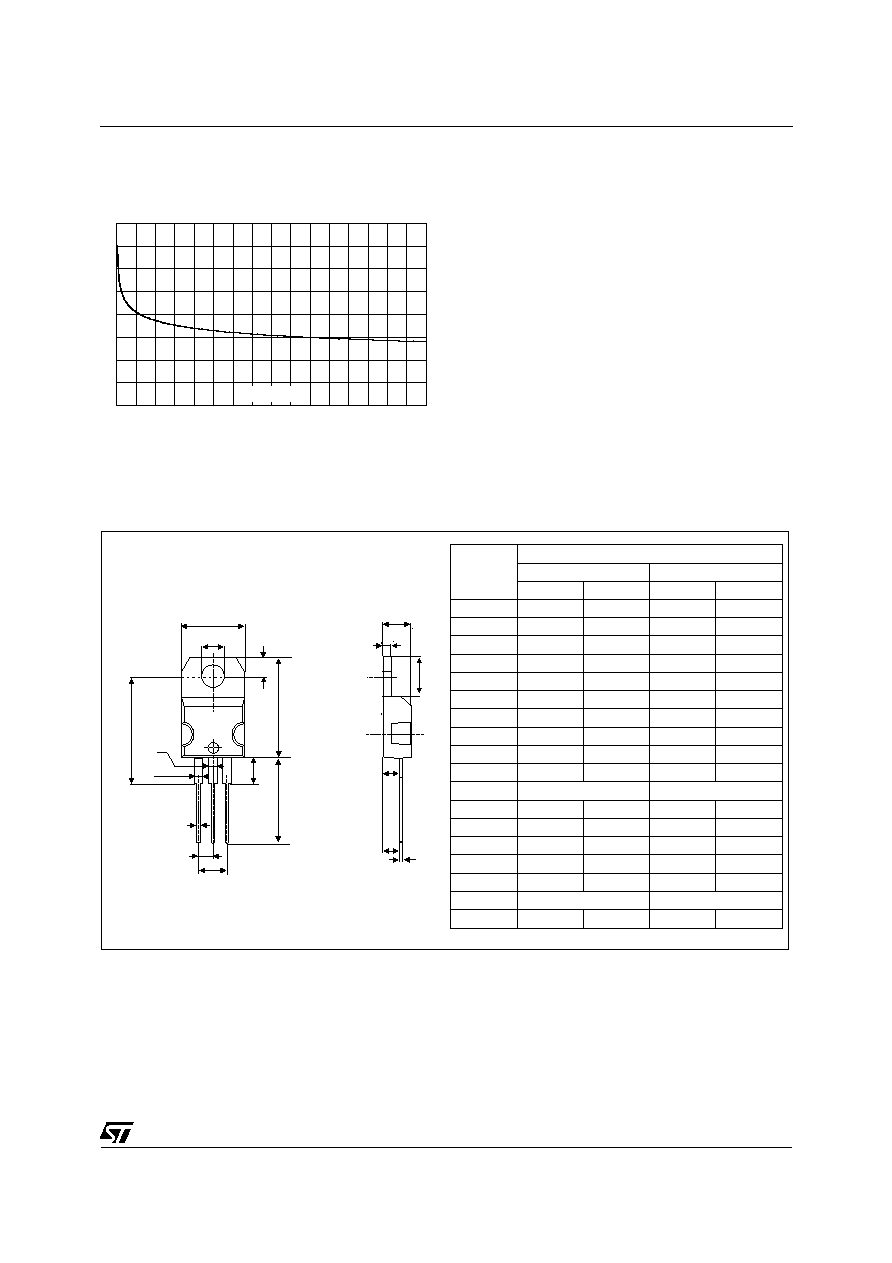
0
10
20
30
40
50
60
70
80
0
5
10
15
20
25
30
35
40
S(cm≤)
R
(∞C/W)
th(j-a)
Fig. 10: Thermal resistance junction to ambient
versus copper surface under tab (epoxy printed
board FR4, Cu=35µm).
PACKAGE MECHANICAL DATA
TO-220AB
A
C
D
L7
Dia
L5
L6
L9
L4
F
H2
G
G1
L2
F2
F1
E
M
REF.
DIMENSIONS
Millimeters
Inches
Min.
Max.
Min.
Max.
A
4.40
4.60
0.173
0.181
C
1.23
1.32
0.048
0.051
D
2.40
2.72
0.094
0.107
E
0.49
0.70
0.019
0.027
F
0.61
0.88
0.024
0.034
F1
1.14
1.70
0.044
0.066
F2
1.14
1.70
0.044
0.066
G
4.95
5.15
0.194
0.202
G1
2.40
2.70
0.094
0.106
H2
10
10.40
0.393
0.409
L2
16.4 typ.
0.645 typ.
L4
13
14
0.511
0.551
L5
2.65
2.95
0.104
0.116
L6
15.25
15.75
0.600
0.620
L7
6.20
6.60
0.244
0.259
L9
3.50
3.93
0.137
0.154
M
2.6 typ.
0.102 typ.
Diam.
3.75
3.85
0.147
0.151