HIGH VOLTAGE POWER SCHOTTKY RECTIFIER
®
1/8
Table 1: Main Product Characteristics
I
F(AV)
2 x 20 A
V
RRM
170 V
T
j
175 °C
V
F
(max)
0.75 V
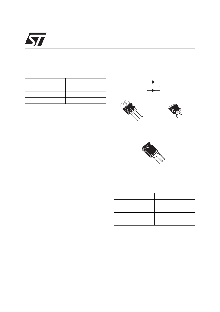
STPS40170C
HIGH VOLTAGE POWER SCHOTTKY RECTIFIER
REV. 1
K
A1
A2
A1
K
K
A2
TO-220AB
STPS40170CT
A1
K
A2
D
2
PAK
STPS40170CG
A1
K
A2
TO-247
STPS40170CW
September 2005
FEATURES AND BENEFITS
High junction temperature capability
Low leakage current
Good trade off between leakage current and
forward voltage drop
Low thermal resistance
High frequency operation
Avalanche specification
DESCRIPTION
Dual center tab Schottky rectifier suited for High
Frequency Switched Mode Power Supplies.
Packaged in TO-220AB, D2PAK and TO-247,
these devices are intended for use to enhance the
reliability of the application.
Table 2: Order Codes
Part Numbers
Marking
STPS40170CT
STPS40170CT
STPS40170CG
STPS40170CG
STPS40170CG-TR
STPS40170CG
STPS40170CW
STPS40170CW
STPS40170C
2/8
Table 3: Absolute Ratings (limiting values, per diode)
Table 4: Thermal Parameters
Table 5: Static Electrical Characteristics (per diode)
Pulse test:
* tp = 5 ms,
< 2%
** tp = 380 µs,
< 2%
To evaluate the conduction losses use the following equation: P = 0.64 x IF(AV) + 0.055 IF
2
(RMS)
Symbol
Parameter
Value
Unit
V
RRM
Repetitive peak reverse voltage
170
V
I
F(RMS)
RMS forward current
60
A
I
F(AV)
Average forward current
T
c
= 150 °C
= 0.5
Per diode
Per device
20
40
A
I
FSM
Surge non repetitive forward current
t
p
= 10 ms sinusoidal
250
A
P
ARM
Repetitive peak avalanche power
t
p
= 1 µs T
j
= 25 °C
14100
W
T
stg
Storage temperature range
-65 to + 175
°C
T
j
Maximum operating junction temperature *
175
°C
dV/dt
Critical rate of rise of reverse voltage
10000
V/µs
* :
thermal runaway condition for a diode on its own heatsink
Symbol
Parameter
Value
Unit
R
th(j-c)
Junction to case
Per diode
Total
1.2
0.85
°C/W
R
th(c)
Coupling
0.5
When the diodes 1 and 2 are used simultaneously:
Tj(diode 1) = P(diode 1) x Rth(j-c)(Per diode) + P(diode 2) x Rth(c)
Symbol
Parameter
Tests conditions
Min.
Typ
Max.
Unit
I
R
*
Reverse leakage current
T
j
= 25 °C
V
R
= V
RRM
30
µA
T
j
= 125 °C
7
30
mA
V
F
**
Forward voltage drop
T
j
= 25 °C
I
F
= 20A
0.92
V
T
j
= 125 °C
0.69
0.75
T
j
= 25 °C
I
F
= 40A
1.00
T
j
= 125 °C
0.79
0.86
dPtot
dTj
---------------
1
Rth j
a
(
)
--------------------------
<
STPS40170C
3/8
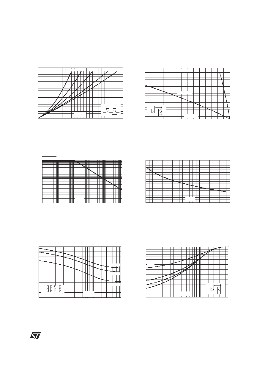
Figure 1: Average forward power dissipation
versus average forward current (per diode)
Figure 2: Average forward current versus
ambient temperature (
= 0.5, per diode)
Figure 3: Normalized avalanche power
derating versus pulse duration
Figure 4: Normalized avalanche power
derating versus junction temperature
Figure 5: Non repetitive surge peak forward
current versus overload duration (maximum
values, per diode)
Figure 6: Relative variation of thermal
impedance junction to case versus pulse
duration
0
2
4
6
8
10
12
14
16
18
20
22
0
2
4
6
8
10
12
14
16
18
20
22
24
26
28
P
F(AV)
(W)
d=0.05
d=0.1
d=0.2
d=0.5
d=1
T
d
=t /T
p
t
p
I
F(AV)
(A)
0
2
4
6
8
10
12
14
16
18
20
22
0
25
50
75
100
125
150
175
I
F(AV)
(A)
R
th(j-a)
=15°C/W
T
d
=t /T
p
t
p
R
th(j-a)
=R
th(j-c)
T
amb
(°C)
0.001
0.01
0.1
0.01
1
0.1
10
100
1000
1
t (µs)
p
P
(t )
P
(1µs)
ARM p
ARM
0
0.2
0.4
0.6
0.8
1
1.2
25
50
75
100
125
150
T (°C)
j
P
(t )
P
(25°C)
ARM p
ARM
0
50
100
150
200
250
1.E-03
1.E-02
1.E-01
1.E+00
I
M
(A)
T
C
=50°C
T
C
=75°C
T
C
=125°C
I
M
t
d =0.5
t(s)
0.0
0.1
0.2
0.3
0.4
0.5
0.6
0.7
0.8
0.9
1.0
1.E-03
1.E-02
1.E-01
1.E+00
Z
th(j-c)
/R
th(j-c)
d=0.1
d=0.2
d=0.5
Single pulse
T
d
=t /T
p
t
p
t
P
(s)
STPS40170C
4/8
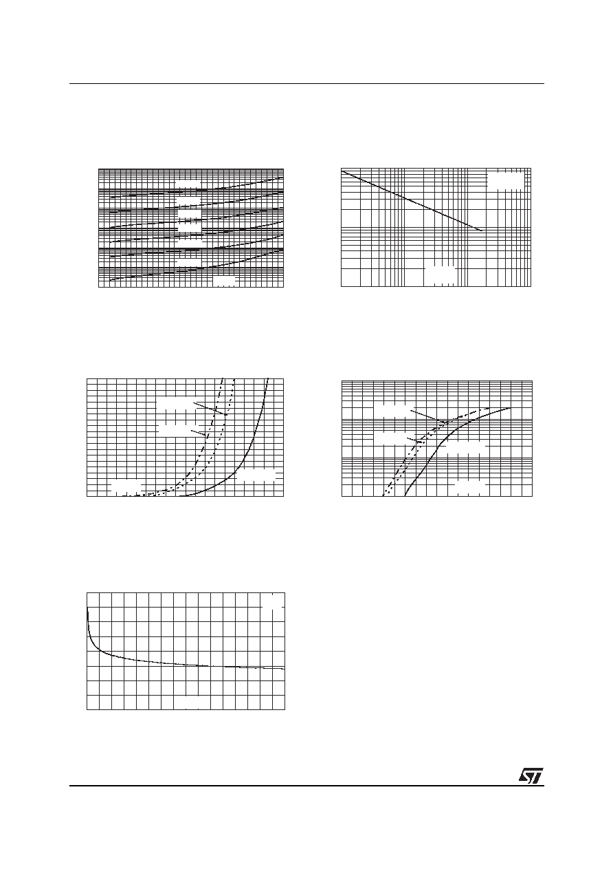
Figure 7: Reverse leakage current versus
reverse voltage applied (typical values, per
diode)
Figure 8: Junction capacitance versus reverse
voltage applied (typical values, per diode)
Figure 9: Forward voltage drop versus forward
current (per diode, low level)
Figure 10: Forward voltage drop versus
forward current (per diode, high level)
Figure 11: Thermal resistance junction to am-
bient versus copper surface under tab (epoxy
printed board FR4, Cu = 35µm) (D
2
PAK)
1.E-01
1.E+00
1.E+01
1.E+02
1.E+03
1.E+04
1.E+05
0
10 20 30 40 50 60 70 80 90 100 110 120 130 140 150 160 170
I
R
(µA)
T
j
=150°C
T
j
=125°C
T
j
=25°C
T
j
=100°C
T
j
=75°C
T
j
=50°C
V
R
(V)
10
100
1000
1
10
100
1000
C(pF)
F=1MHz
V
OSC
=30mV
RMS
T
j
=25°C
V
R
(V)
I
FM
(A)
V
FM
(V)
0
2
4
6
8
10
12
14
16
18
20
0.0
0.1
0.2
0.3
0.4
0.5
0.6
0.7
0.8
0.9
1.0
Tj=25°C
(Maximum values)
Tj=125°C
(Maximum values)
Tj=125°C
(Maximum values)
Tj=125°C
(Typical values)
Tj=125°C
(Typical values)
I
FM
(A)
1
10
100
1000
0.0
0.2
0.4
0.6
0.8
1.0
1.2
1.4
1.6
1.8
Tj=25°C
(Maximum values)
Tj=125°C
(Maximum values)
Tj=125°C
(Maximum values)
Tj=125°C
(Typical values)
Tj=125°C
(Typical values)
V
FM
(V)
0
10
20
30
40
50
60
70
80
0
5
10
15
20
25
30
35
40
R
th(j-a)
(°C/W)
D²PAK
S
CU
(cm²)
STPS40170C
5/8
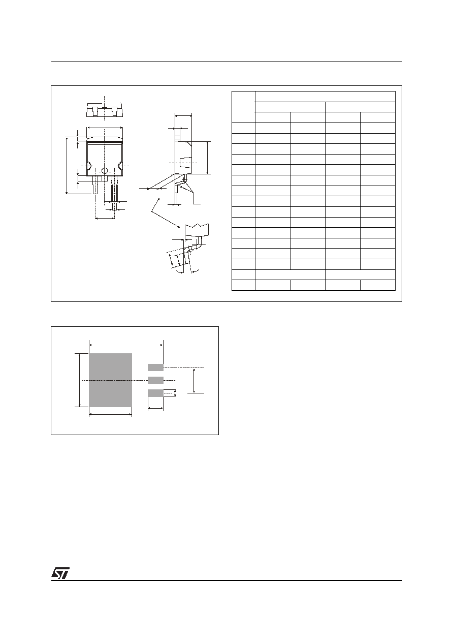
Figure 12: D
2
PAK Package Mechanical Data
Figure 13: Foot Print Dimensions (in millimeters)
G
L
L3
L2
B
B2
E
* FLAT ZONE NO LESS THAN 2mm
A
C2
D
R
A2
M
V2
C
A1
*
16.90
10.30
8.90
3.70
5.08
1.30
REF.
DIMENSIONS
Millimeters
Inches
Min.
Max.
Min.
Max.
A
4.40
4.60
0.173
0.181
A1
2.49
2.69
0.098
0.106
A2
0.03
0.23
0.001
0.009
B
0.70
0.93
0.027
0.037
B2
1.14
1.70
0.045
0.067
C
0.45
0.60
0.017
0.024
C2
1.23
1.36
0.048
0.054
D
8.95
9.35
0.352
0.368
E
10.00
10.40
0.393
0.409
G
4.88
5.28
0.192
0.208
L
15.00
15.85
0.590
0.624
L2
1.27
1.40
0.050
0.055
L3
1.40
1.75
0.055
0.069
M
2.40
3.20
0.094
0.126
R
0.40 typ.
0.016 typ.
V2
0°
8°
0°
8°