Æ
1/6
Table 1: Main Product Characteristics
I
F(AV)
2 x 30 A
V
RRM
170 V
T
j
175 ∞C
V
F
(max)
0.76 V
STPS60170C
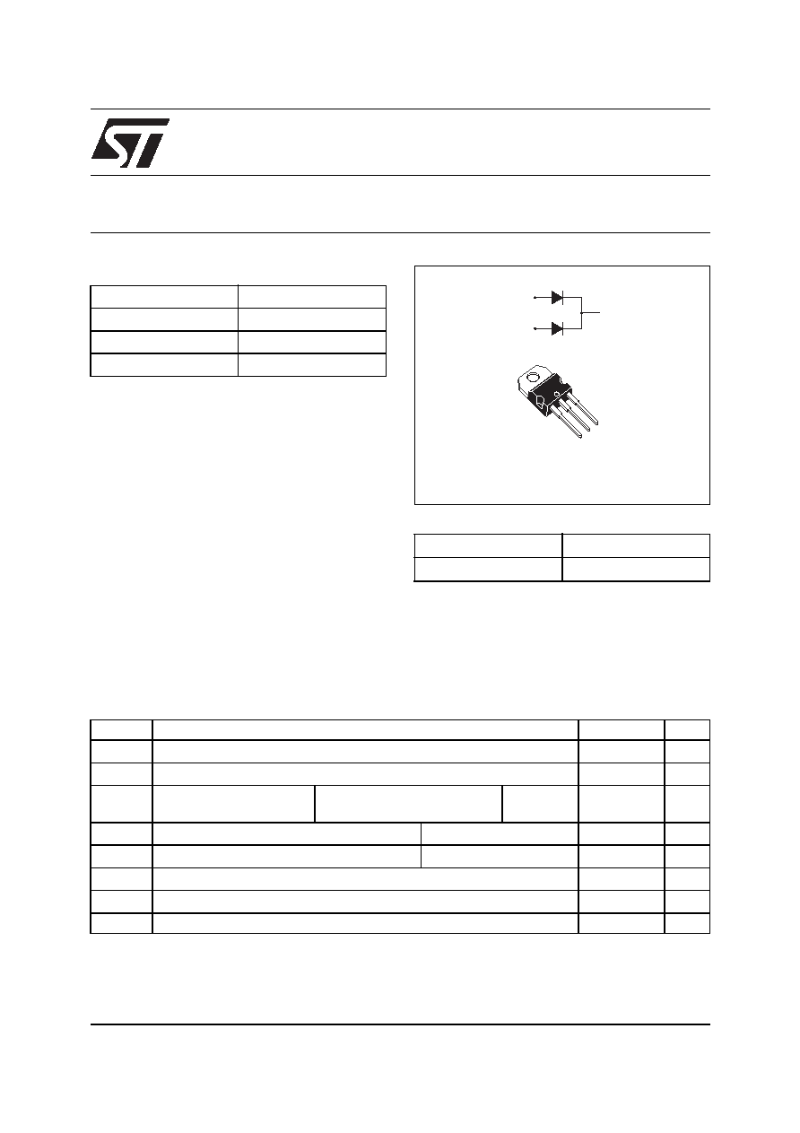
HIGH VOLTAGE POWER SCHOTTKY RECTIFIER
REV. 1
K
A1
A2
A1
K
K
A2
TO-220AB
STPS60170CT
September 2005
FEATURES AND BENEFITS
High junction temperature capability
Low leakage current
Good trade off between leakage current and
forward voltage drop
Low thermal resistance
High frequency operation
Avalanche specification
DESCRIPTION
Dual center tab Schottky rectifier suited for High
Frequency Switched Mode Power Supplies.
Packaged in TO-220AB, this device is intended for
use to enhance the reliability of the application.
Table 2: Order Code
Part Number
Marking
STPS60170CT
STPS60170CT
Table 3: Absolute Ratings (limiting values, per diode)
Symbol
Parameter
Value
Unit
V
RRM
Repetitive peak reverse voltage
170
V
I
F(RMS)
RMS forward current
60
A
I
F(AV)
Average forward current
T
c
= 150 ∞C
= 0.5
Per diode
Per device
30
60
A
I
FSM
Surge non repetitive forward current
t
p
= 10 ms sinusoidal
270
A
P
ARM
Repetitive peak avalanche power
t
p
= 1 µs T
j
= 25 ∞C
17300
W
T
stg
Storage temperature range
-65 to + 175
∞C
T
j
Maximum operating junction temperature *
175
∞C
dV/dt
Critical rate of rise of reverse voltage
10000
V/µs
* :
thermal runaway condition for a diode on its own heatsink
dPtot
dTj
---------------
1
Rth j
a
≠
(
)
--------------------------
<
STPS60170C
2/6
Table 4: Thermal Parameters
Table 5: Static Electrical Characteristics (per diode)
Pulse test:
* tp = 5 ms,
< 2%
** tp = 380 µs,
< 2%
To evaluate the conduction losses use the following equation: P = 0.60 x IF(AV) + 0.053 IF
2
(RMS)
Symbol
Parameter
Value
Unit
R
th(j-c)
Junction to case
Per diode
Total
1.0
0.7
∞C/W
R
th(c)
Coupling
0.4
When the diodes 1 and 2 are used simultaneously:
Tj(diode 1) = P(diode 1) x Rth(j-c)(Per diode) + P(diode 2) x Rth(c)
Symbol
Parameter
Tests conditions
Min.
Typ
Max.
Unit
I
R
*
Reverse leakage current
T
j
= 25 ∞C
V
R
= V
RRM
35
µA
T
j
= 125 ∞C
8
35
mA
V
F
**
Forward voltage drop
T
j
= 25 ∞C
I
F
= 30 A
0.94
V
T
j
= 125 ∞C
0.72
0.76
T
j
= 25 ∞C
I
F
= 60 A
0.97
1.05
T
j
= 125 ∞C
0.86
0.92
STPS60170C
3/6
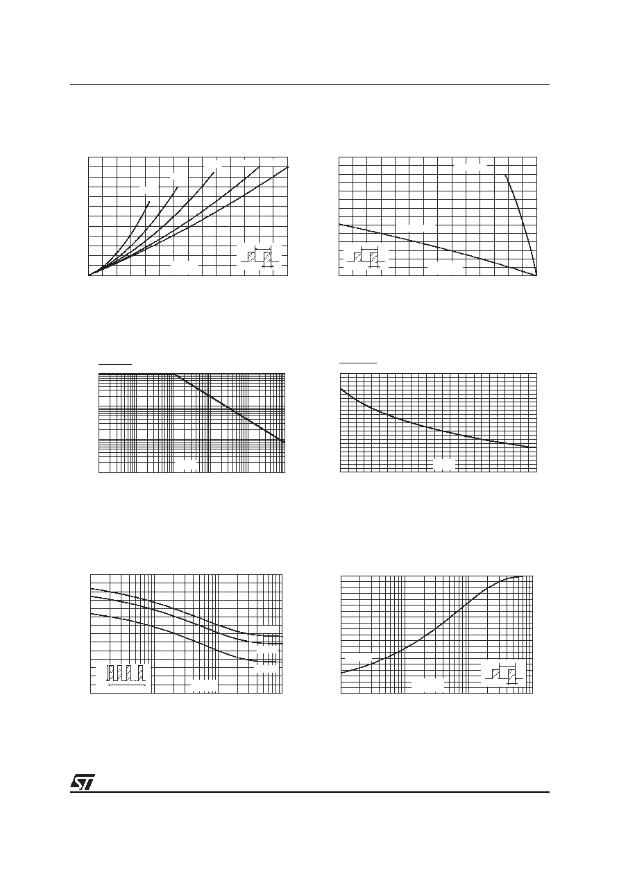
Figure 1: Average forward power dissipation
versus average forward current (per diode)
Figure 2: Average forward current versus
ambient temperature (
= 0.5, per diode)
Figure 3: Normalized avalanche power
derating versus pulse duration
Figure 4: Normalized avalanche power
derating versus junction temperature
Figure 5: Non repetitive surge peak forward
current versus overload duration (maximum
values, per diode)
Figure 6: Relative variation of thermal
impedance junction to case versus pulse
duration
0
5
10
15
20
25
30
0
5
10
15
20
25
30
35
P
F(AV)
(W)
d=0.05
d=0.1
d=0.2
d=0.5
d=1
T
d
=t /T
p
t
p
I
F(AV)
(A)
0
5
10
15
20
25
30
35
0
25
50
75
100
125
150
175
I
F(AV)
(A)
R
th(j-a)
=15∞C/W
T
d
=t /T
p
t
p
R
th(j-a)
=R
th(j-c)
T
amb
(∞C)
0.001
0.01
0.1
0.01
1
0.1
10
100
1000
1
t (µs)
p
P
(t )
P
(1µs)
ARM p
ARM
0
0.2
0.4
0.6
0.8
1
1.2
25
50
75
100
125
150
T (∞C)
j
P
(t )
P
(25∞C)
ARM p
ARM
0
50
100
150
200
250
300
350
1.E-03
1.E-02
1.E-01
1.E+00
I
M
(A)
T
C
=50∞C
T
C
=75∞C
T
C
=125∞C
I
M
t
d =0.5
t(s)
0.0
0.1
0.2
0.3
0.4
0.5
0.6
0.7
0.8
0.9
1.0
1.E-03
1.E-02
1.E-01
1.E+00
Z
th(j-c)
/R
th(j-c)
Single pulse
T
d
=t /T
p
t
p
t
P
(s)
STPS60170C
4/6
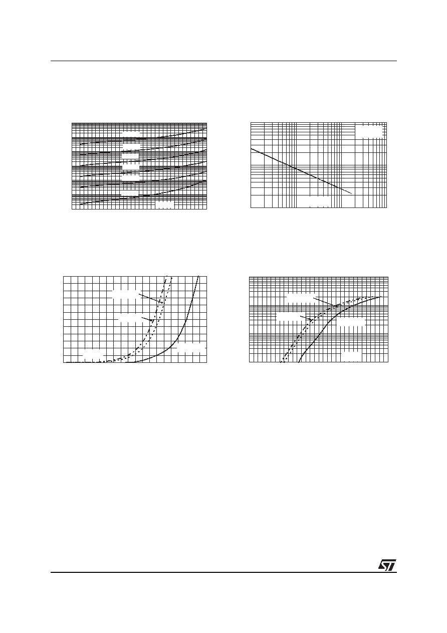
Figure 7: Reverse leakage current versus
reverse voltage applied (typical values, per
diode)
Figure 8: Junction capacitance versus reverse
voltage applied (typical values, per diode)
Figure 9: Forward voltage drop versus forward
current (per diode, low level)
Figure 10: Forward voltage drop versus
forward current (per diode, high level)
1.E-01
1.E+00
1.E+01
1.E+02
1.E+03
1.E+04
1.E+05
0
10 20 30 40 50 60 70 80 90 100 110 120 130 140 150 160 170
I
R
(µA)
T
j
=150∞C
T
j
=125∞C
T
j
=25∞C
T
j
=100∞C
T
j
=75∞C
T
j
=50∞C
V
R
(V)
C(pF)
100
1000
10000
1
10
100
1000
F=1MHz
V
OSC
=30mV
RMS
T
j
=25∞C
V
R
(V)
I
FM
(A)
0
5
10
15
20
25
30
0.0
0.1
0.2
0.3
0.4
0.5
0.6
0.7
0.8
0.9
1.0
Tj=25∞C
(Maximum values)
Tj=125∞C
(Maximum values)
Tj=125∞C
(Maximum values)
Tj=125∞C
(Typical values)
Tj=125∞C
(Typical values)
V
FM
(V)
I
FM
(A)
1
10
100
1000
0.0 0.1 0.2 0.3 0.4 0.5 0.6 0.7 0.8 0.9 1.0 1.1 1.2 1.3 1.4 1.5 1.6
Tj=25∞C
(Maximum values)
Tj=125∞C
(Maximum values)
Tj=125∞C
(Maximum values)
Tj=125∞C
(Typical values)
Tj=125∞C
(Typical values)
V
FM
(V)
STPS60170C
5/6
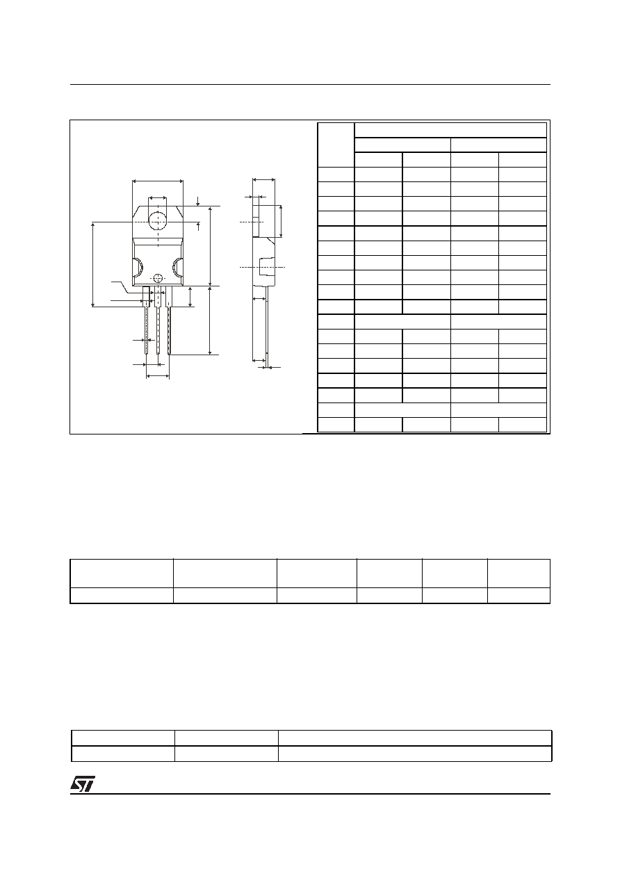
Figure 11: TO-220AB Package Mechanical Data
In order to meet environmental requirements, ST offers these devices in ECOPACKÆ packages. These
packages have a Lead-free second level interconnect . The category of second level interconnect is
marked on the package and on the inner box label, in compliance with JEDEC Standard JESD97. The
maximum ratings related to soldering conditions are also marked on the inner box label. ECOPACK is an
ST trademark. ECOPACK specifications are available at: www.st.com.
A
C
D
L7
Dia
L5
L6
L9
L4
F
H2
G
G1
L2
F2
F1
E
M
REF.
DIMENSIONS
Millimeters
Inches
Min.
Max.
Min.
Max.
A
4.40
4.60
0.173
0.181
C
1.23
1.32
0.048
0.051
D
2.40
2.72
0.094
0.107
E
0.49
0.70
0.019
0.027
F
0.61
0.88
0.024
0.034
F1
1.14
1.70
0.044
0.066
F2
1.14
1.70
0.044
0.066
G
4.95
5.15
0.194
0.202
G1
2.40
2.70
0.094
0.106
H2
10
10.40
0.393
0.409
L2
16.4 typ.
0.645 typ.
L4
13
14
0.511
0.551
L5
2.65
2.95
0.104
0.116
L6
15.25
15.75
0.600
0.620
L7
6.20
6.60
0.244
0.259
L9
3.50
3.93
0.137
0.154
M
2.6 typ.
0.102 typ.
Diam.
3.75
3.85
0.147
0.151
Table 6: Ordering Information
Epoxy meets UL94, V0
Cooling method: by conduction (C)
Recommended torque value: 0.55 Nm.
Maximum torque value: 0.7 Nm.
Ordering type
Marking
Package
Weight
Base qty
Delivery
mode
STPS60170CT
STPS60170CT
TO-220AB
2.20 g
50
Tube
Table 7: Revision History
Date
Revision
Description of Changes
16-Sep-2005
1
First issue.