Æ
1/5
Table 1: Main Product Characteristics
I
F(AV)
2 x 30 A
V
RRM
170 V
T
j
175 ∞C
V
F
(max)
0.67 V
STPS61170C
HIGH VOLTAGE POWER SCHOTTKY RECTIFIER
REV. 1
Table 3: Absolute Ratings (limiting values, per diode)
Symbol
Parameter
Value
Unit
V
RRM
Repetitive peak reverse voltage
170
V
I
F(RMS)
RMS forward current
80
A
I
F(AV)
Average forward current
Tc = 150 ∞C
= 0.5
Per diode
Per device
30
60
A
I
FSM
Surge non repetitive forward current
tp = 10 ms sinusoidal
500
A
P
ARM
Repetitive peak avalanche power
tp = 1 µs Tj = 25 ∞C
31800
W
T
stg
Storage temperature range
-65 to + 175
∞C
T
j
Maximum operating junction temperature *
175
∞C
dV/dt
Critical rate of rise of reverse voltage
10000
V/µs
* :
thermal runaway condition for a diode on its own heatsink
dPtot
dTj
---------------
1
Rth j
a
≠
(
)
--------------------------
>
K
A1
A2
A1
K
A2
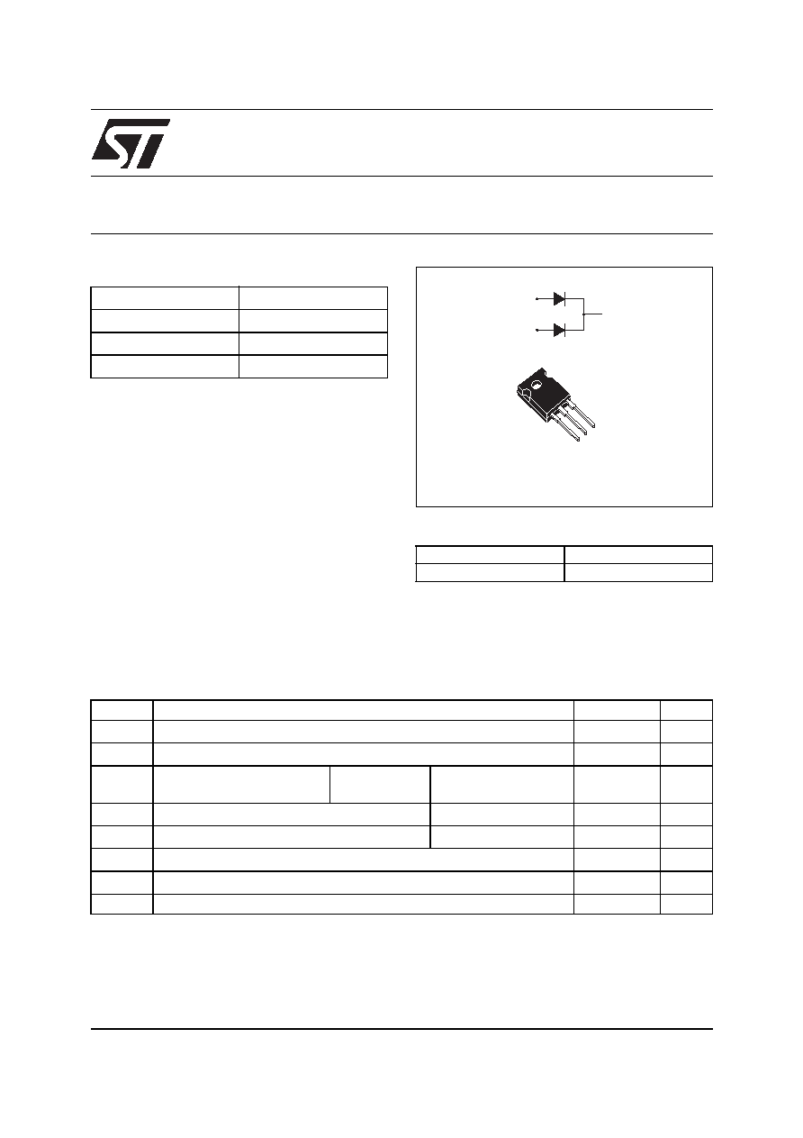
TO-247
September 2005
FEATURES AND BENEFITS
High junction temperature capability
Low leakage current
Good trade off between leakage current and
forward voltage drop
Low thermal resistance
High frequency operation
Avalanche specification
DESCRIPTION
Dual center tab Schottky rectifier suited for High
Frequency Switch Mode Power Supply.
Packaged in TO-247, this device is intended for
use to enhance the reliability of the application.
Table 2: Order Code
Part Number
Marking
STPS61170CW
STPS61170CW
STPS61170C
2/5
Table 4: Thermal Parameters
Table 5: Static Electrical Characteristics (per diode)
Pulse test:
* tp = 5 ms,
< 2%
** tp = 380 µs,
< 2%
To evaluate the conduction losses use the following equation: P = 0.54 x IF(AV) + 0.0043 IF
2
(RMS)
Symbol
Parameter
Value
Unit
R
th(j-c)
Junction to case
Per diode
Total
0.9
0.6
∞C/W
R
th(c)
Coupling
0.3
When the diodes 1 and 2 are used simultaneously:
Tj(diode 1) = P(diode 1) x Rth(j-c)(Per diode) + P(diode 2) x Rth(c)
Symbol
Parameter
Tests conditions
Min.
Typ
Max.
Unit
I
R
*
Reverse leakage current
T
j
= 25 ∞C
V
R
= V
RRM
60
µA
T
j
= 125 ∞C
16
60
mA
V
F
**
Forward voltage drop
T
j
= 25 ∞C
I
F
= 30 A
0.84
V
T
j
= 125 ∞C
I
F
= 30 A
0.63
0.67
T
j
= 25 ∞C
I
F
= 60 A
0.92
T
j
= 125 ∞C
I
F
= 60 A
0.76
0.80
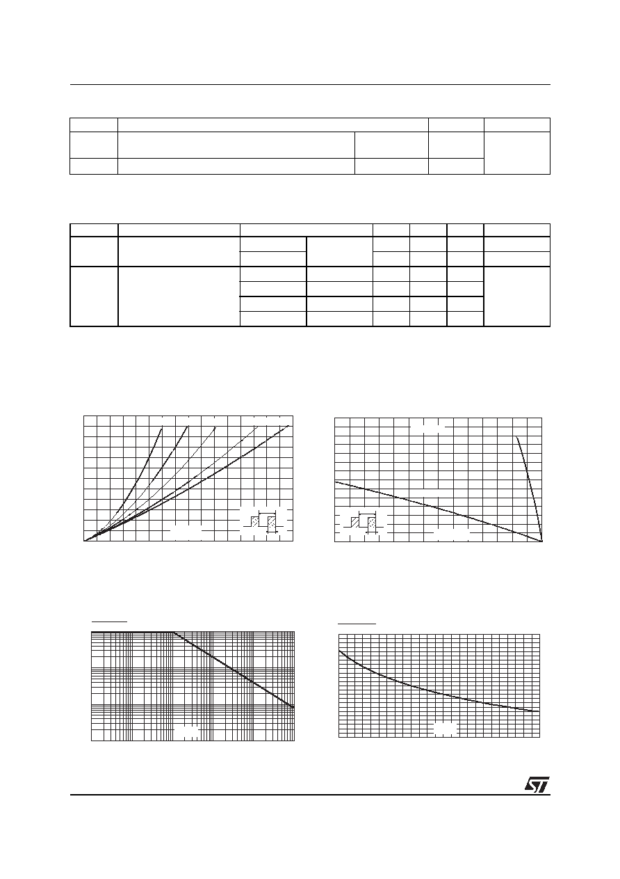
Figure 1: Average forward power dissipation
versus average forward current (per diode)
Figure 2: Average forward current versus
ambient temperature (
= 0.5, per diode)
Figure 3: Normalized avalanche power
derating versus pulse duration
Figure 4: Normalized avalanche power
derating versus junction temperature
0
5
10
15
20
25
30
0
5
10
15
20
25
30
35
40
P
F(AV)
(W)
d=0.05
d=0.1
d=0.2
d=0.5
d=1
T
d
=t /T
p
t
p
I
F(AV)
(A)
0
5
10
15
20
25
30
35
0
25
50
75
100
125
150
175
I
F(AV)
(A)
R
th(j-a)
=15∞C/W
T
d=t /T
p
t
p
R
th(j-a)
=R
th(j-c)
T
amb
(∞C)
0.001
0.01
0.1
0.01
1
0.1
10
100
1000
1
t (µs)
p
P
(t )
P
(1µs)
ARM p
ARM
0
0.2
0.4
0.6
0.8
1
1.2
25
50
75
100
125
150
T (∞C)
j
P
(t )
P
(25∞C)
ARM p
ARM
STPS61170C
3/5
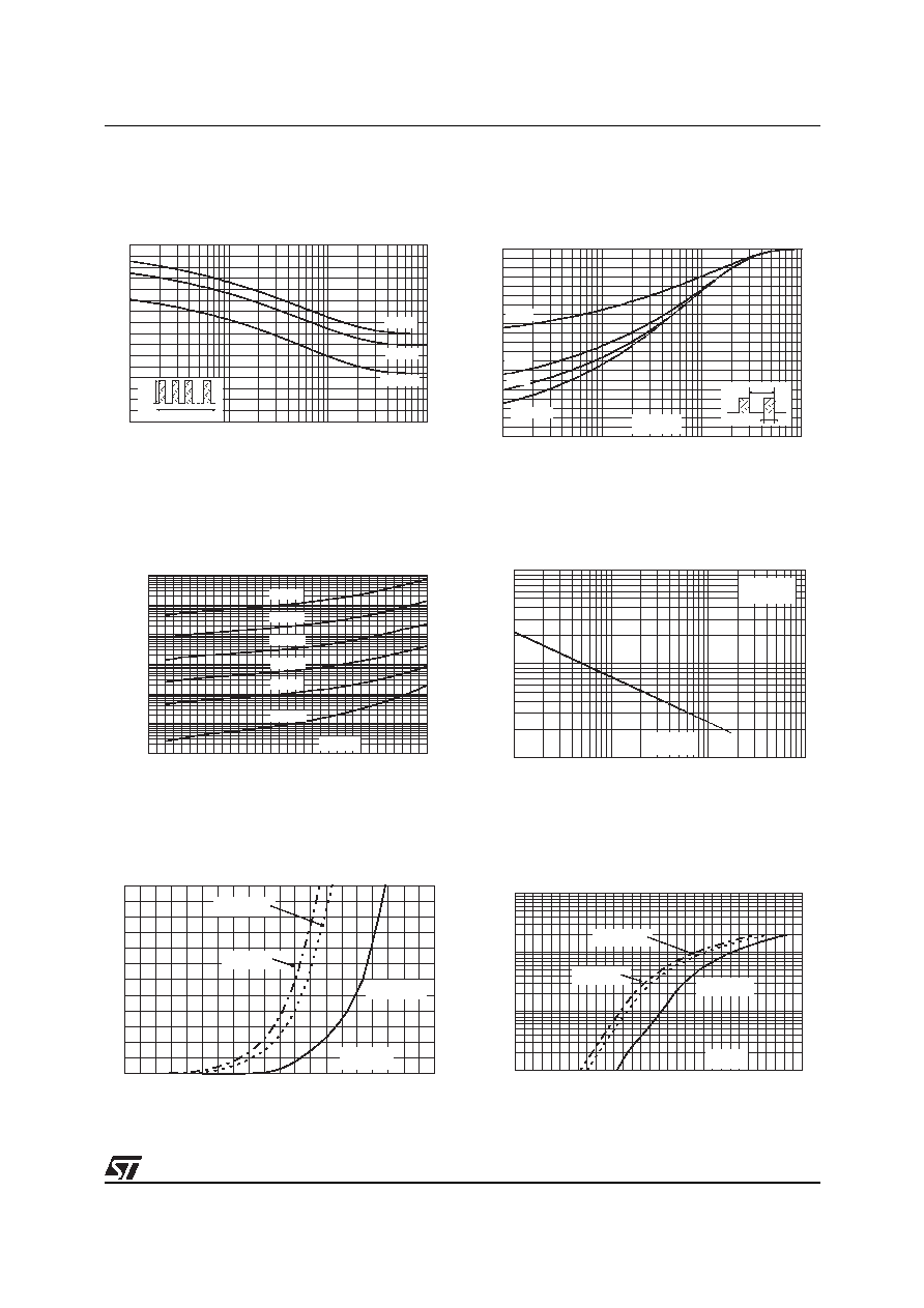
Figure 5: Non repetitive surge peak forward
current versus overload duration (maximum
values, per diode)
Figure 6: Relative variation of thermal
impedance junction to case versus pulse
duration (per diode)
Figure 7: Reverse leakage current versus
reverse voltage applied (typical values, per
diode)
Figure 8: Junction capacitance versus reverse
voltage applied (typical values, per diode)
Figure 9: Forward voltage drop versus forward
current (per diode, low level)
Figure 10: Forward voltage drop versus for-
ward current (per diode, high level)
0
50
100
150
200
250
300
350
400
1.E-03
1.E-02
1.E-01
1.E+00
t(s)
I
M
(A)
T
C
=50∞C
T
C
=75∞C
T
C
=125∞C
I
M
t
d =0.5
0.0
0.1
0.2
0.3
0.4
0.5
0.6
0.7
0.8
0.9
1.0
1.E-03
1.E-02
1.E-01
1.E+00
Z
th(j-c)
/R
th(j-c)
d=0.1
d=0.2
d=0.5
Single pulse
T
d
=t /T
p
t
p
t
P
(s)
1.E-01
1.E+00
1.E+01
1.E+02
1.E+03
1.E+04
1.E+05
0
10 20 30 40 50 60 70 80 90 100 110 120 130 140 150 160 170
I
R
(µA)
T
j
=150∞C
T
j
=125∞C
T
j
=25∞C
T
j
=100∞C
T
j
=75∞C
T
j
=50∞C
V
R
(V)
100
1000
10000
1
10
100
1000
C(pF)
F=1MHz
V
OSC
=30mV
RMS
T
j
=25∞C
V
R
(V)
I
FM
(A)
0
5
10
15
20
25
30
0.0
0.1
0.2
0.3
0.4
0.5
0.6
0.7
0.8
0.9
1.0
Tj=25∞C
(Maximum values)
Tj=125∞C
(Maximum values)
Tj=125∞C
(Maximum values)
Tj=125∞C
(Typical values)
Tj=125∞C
(Typical values)
V
FM
(V)
I
FM
(A)
1
10
100
1000
0.0 0.1 0.2 0.3 0.4 0.5 0.6 0.7 0.8 0.9 1.0 1.1 1.2 1.3 1.4 1.5 1.6
Tj=25∞C
(Maximum values)
Tj=125∞C
(Maximum values)
Tj=125∞C
(Maximum values)
Tj=125∞C
(Typical values)
Tj=125∞C
(Typical values)
V
FM
(V)
STPS61170C
4/5
Figure 11: TO-247 Package Mechanical Data
In order to meet environmental requirements, ST offers these devices in ECOPACKÆ packages. These
packages have a Lead-free second level interconnect . The category of second level interconnect is
marked on the package and on the inner box label, in compliance with JEDEC Standard JESD97. The
maximum ratings related to soldering conditions are also marked on the inner box label. ECOPACK is an
ST trademark. ECOPACK specifications are available at: www.st.com.
H
L2
L5
L
L4
D
E
M
L1
L3
F2
F3
F4
F1
V2
F(x3)
G
A
V
V
Dia
Table 6: Ordering Information
Epoxy meets UL94, V0
Cooling method: by conduction (C)
Recommended torque value: 0.8 Nm.
Maximum torque value: 1.0 Nm.
Ordering type
Marking
Package
Weight
Base qty
Delivery
mode
STPS61170CW
STPS61170CW
TO-247
4.40 g
30
Tube
Table 7: Revision History
Date
Revision
Description of Changes
16-Sep-2005
1
First issue.
REF.
DIMENSIONS
Millimeters
Inches
Min.
Typ.
Max.
Min.
Typ.
Max.
A
4.85
5.15
0.191
0.203
D
2.20
2.60
0.086
0.102
E
0.40
0.80
0.015
0.031
F
1.00
1.40
0.039
0.055
F1
3.00
0.118
F2
2.00
0.078
F3
2.00
2.40
0.078
0.094
F4
3.00
3.40
0.118
0.133
G
10.90
0.429
H
15.45
15.75 0.608
0.620
L
19.85
20.15 0.781
0.793
L1
3.70
4.30
0.145
0.169
L2
18.50
0.728
L3
14.20
14.80 0.559
0.582
L4
34.60
1.362
L5
5.50
0.216
M
2.00
3.00
0.078
0.118
V
5∞
5∞
V2
60∞
60∞
Dia.
3.55
3.65
0.139
0.143

STPS61170C
5/5
Information furnished is believed to be accurate and reliable. However, STMicroelectronics assumes no responsibility for the consequences
of use of such information nor for any infringement of patents or other rights of third parties which may result from its use. No license is granted
by implication or otherwise under any patent or patent rights of STMicroelectronics. Specifications mentioned in this publication are subject
to change without notice. This publication supersedes and replaces all information previously supplied. STMicroelectronics products are not
authorized for use as critical components in life support devices or systems without express written approval of STMicroelectronics.
The ST logo is a registered trademark of STMicroelectronics.
All other names are the property of their respective owners
© 2005 STMicroelectronics - All rights reserved
STMicroelectronics group of companies
Australia - Belgium - Brazil - Canada - China - Czech Republic - Finland - France - Germany - Hong Kong - India - Israel - Italy - Japan -
Malaysia - Malta - Morocco - Singapore - Spain - Sweden - Switzerland - United Kingdom - United States of America
www.st.com