1/5
STPS80L15CY
PRELIMINARY DATASHEET
Æ
July 2003 - Ed: 5B
LOW DROP OR-ing POWER SCHOTTKY RECTIFIER
I
F(AV)
2 x 40 A
V
RRM
15 V
Tj (max)
125 ∞C
V
F
(max)
0.33 V
MAIN PRODUCT CHARACTERISTICS
n
Max247
PACKAGE,
DUAL
DIODE
CONSTRUCTION, 2 x 40A
n
15V BLOCKING VOLTAGE SUITABLE FOR 5V
AND 12V OR-ing
n
EXTREMELY
LOW
VOLTAGE
VOLTAGE
DROP: 0.33V @ 100∞C
n
OPERATING
JUNCTION
TEMPERATURE:
125∞C
n
AVALANCHE CAPABILITY SPECIFIED
FEATURES AND BENEFITS
The STPS80L15CY uses proprietary barrier
technology to optimize forward voltage drop for
OR-ing functions in n-1 fault tolerant Switch Mode
Power Supplies.
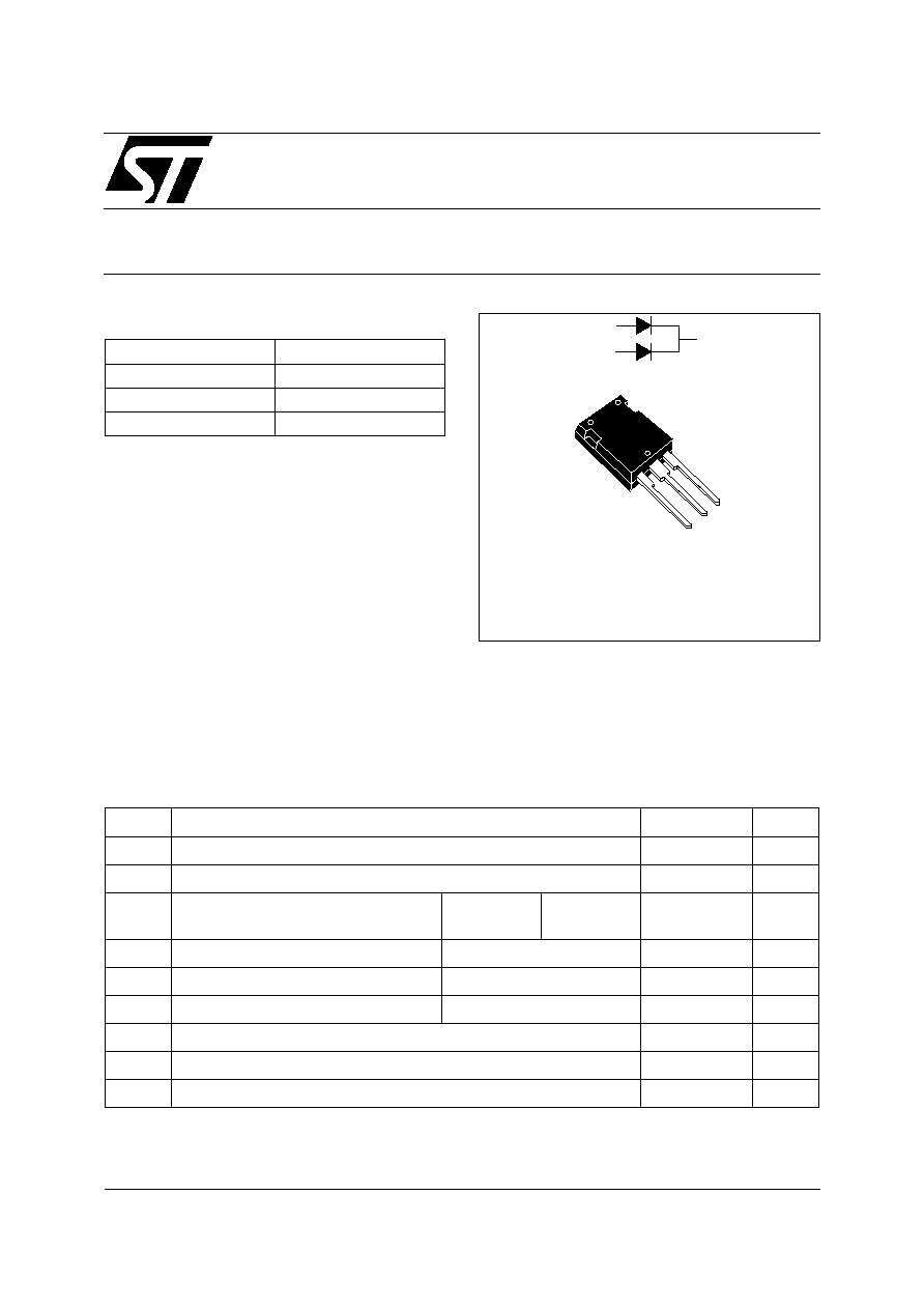
DESCRIPTION
Max247
A1
K
A2
Symbol
Parameter
Value
Unit
V
RRM
Repetitive peak reverse voltage
15
V
I
F(RMS)
RMS forward current
50
A
I
F(AV)
Average forward current
Tc = 110∞C
= 0.5
Per diode
Per device
40
80
A
I
FSM
Surge non repetitive forward current
tp = 10 ms sinusoidal
400
A
I
RRM
Repetitive peak reverse current
tp = 2 µs F = 1kHz square
2
A
P
ARM
Repetitive peak avalanche power
tp = 1µs
Tj = 25∞C
36045
W
T
stg
Storage temperature range
- 65 to + 150
∞
C
Tj
Maximum operating junction temperature
125
∞C
dV/dt
Critical rate of rise of reverse voltage
10000
V/µs
ABSOLUTE RATINGS (limiting values, per diode)
A1
A2
K
STPS80L15CY
2/5
Symbol
Parameter
Value
Unit
R
th (j-c)
Junction to case
Per diode
0.7
∞
C/W
Total
0.5
R
th (c)
Coupling
0.3
THERMAL RESISTANCES
Symbol
Parameter
Tests conditions
Min.
Typ.
Max.
Unit
I
R
*
Reverse leakage current
Tj = 25
∞
C
V
R
= 5V
4
mA
Tj = 100
∞
C
280
400
Tj = 25
∞
C
V
R
= 12V
11
Tj = 100
∞
C
0.44
1.1
A
Tj = 25
∞
C
V
R
= 15V
16
mA
Tj = 100
∞
C
0.53
1.3
A
V
F
*
Forward voltage drop
Tj = 25
∞
C
I
F
= 40 A
0.42
V
Tj = 100
∞
C
I
F
= 40 A
0.30
0.33
Tj = 25
∞
C
I
F
= 80 A
0.55
Tj = 100
∞
C
I
F
= 80 A
0.40
0.46
Pulse test :* tp = 380 µs,
< 2%
To evaluate the maximum conduction losses use the following equation :
P = 0.20 x I
F(AV)
+ 0.0032 x I
F
2
(RMS)
STATIC ELECTRICAL CHARACTERISTICS (per diode)
When the diodes 1 and 2 are used simultaneously :
Tj(diode 1) = P(diode1) x R
th(j-c)
(Per diode) + P(diode 2) x R
th(c)
STPS80L15CY
3/5
0
5
10
15
20
25
30
35
40
45
50
55
60
0
2
4
6
8
10
12
14
16
18
20
22
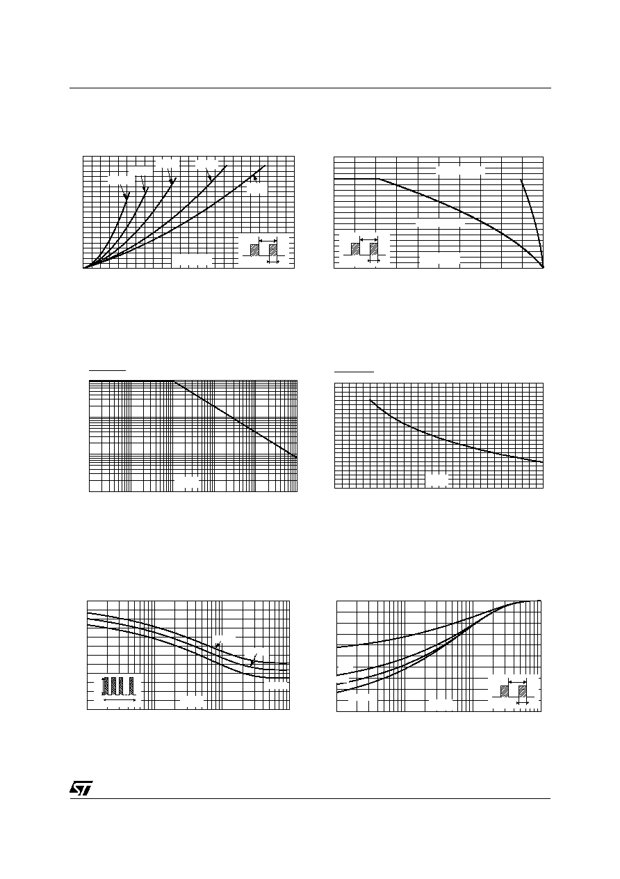
PF(av)(W)
= 0.2
= 0.5
= 1
= 0.05
= 0.1
IF(av) (A)
T
=tp/T
tp
Fig. 1: Average forward power dissipation versus
average forward current (per diode).
0
25
50
75
100
125
0
5
10
15
20
25
30
35
40
45
50
IF(av)(A)
Rth(j-a)=5∞C/W
Rth(j-a)=Rth(j-c)
Tamb(∞C)
T
=tp/T
tp
Fig. 2: Average forward current versus ambient
temperature (
=0.5, per diode).
0.001
0.01
0.1
0.01
1
0.1
10
100
1000
1
t (µs)
p
P
(t )
P
(1µs)
ARM p
ARM
Fig. 3: Normalized avalanche power derating
versus pulse duration.
0
0.2
0.4
0.6
0.8
1
1.2
0
25
50
75
100
125
150
T (∞C)
j
P
(t )
P
(25∞C)
ARM p
ARM
Fig. 4: Normalized avalanche power derating
versus junction temperature.
1E-3
1E-2
1E-1
1E+0
0
100
200
300
400
500
600
IM(A)
Tc=75∞C
Tc=25∞C
Tc=50∞C
t(s)
I
M
t
=0.5
Fig. 5: Non repetitive surge peak forward current
versus overload duration (maximum values, per
diode).
1E-3
1E-2
1E-1
1E+0
0.0
0.2
0.4
0.6
0.8
1.0
Zth(j-c)/Rth(j-c)
=0.1
=0.2
=0.5
Single pulse
tp(s)
T
=tp/T
tp
Fig. 6: Relative variation of thermal impedance
junction to case versus pulse (per diode).

STPS80L15CY
4/5
0
1
2
3
4
5
6
7
8
9 10 11 12 13 14 15
1E-1
1E+0
1E+1
1E+2
1E+3
IR(mA)
Tj=25∞C
Tj=75∞C
VR(V)
Tj=100∞C
Fig. 7: Reverse leakage current versus reverse
voltage applied (typical values, per diode).
1
2
5
10
20
1
2
5
10
C(nF)
F=1MHz
Tj=25∞C
VR(V)
Fig. 8: Junction capacitance versus reverse
voltage applied (typical values, per diode).
0.0
0.1
0.2
0.3
0.4
0.5
0.6
0.7
0.8
1
10
100
200
IFM(A)
Tj=100∞C
(typical values)
Tj=25∞C
(Maximum values)
Tj=100∞C
(Maximum values)
VFM(V)
Fig. 9: Forward voltage drop versus forward
current (per diode).
STPS80L15CY
5/5
Information furnished is believed to be accurate and reliable. However, STMicroelectronics assumes no responsibility for the consequences of
use of such information nor for any infringement of patents or other rights of third parties which may result from its use. No license is granted by
implication or otherwise under any patent or patent rights of STMicroelectronics. Specifications mentioned in this publication are subject to
change without notice. This publication supersedes and replaces all information previously supplied.
STMicroelectronics products are not authorized for use as critical components in life support devices or systems without express written
approval of STMicroelectronics.
The ST logo is a registered trademark of STMicroelectronics
© 2003 STMicroelectronics - Printed in Italy - All rights reserved.
STMicroelectronics GROUP OF COMPANIES
Australia - Brazil - Canada - China - Finland - France - Germany
Hong Kong - India - Israel - Italy - Japan - Malaysia - Malta - Morocco - Singapore
Spain - Sweden - Switzerland - United Kingdom - United States.
http://www.st.com
PACKAGE MECHANICAL DATA
Max247
A
E
e
L1
b1
b2
b
L
D
c
A1
REF.
DIMENSIONS
Millimeters
Inches
Min.
Max.
Min.
Max.
A
4.70
5.30
0.185
0.209
A1
2.20
2.60
0.087
0.102
b
1.00
1.40
0.038
0.055
b1
2.00
2.40
0.079
0.094
b2
3.00
3.40
0.118
0.133
c
0.40
0.80
0.016
0.031
D
19.70
10.30
0.776
0.799
e
5.35
5.55
0.211
0.219
E
15.30
15.90
0.602
0.626
L
14.20
15.20
0.559
0.598
L1
3.70
4.30
0.146
0.169
Ordering type
Marking
Package
Weight
Base qty
Delivery mode
STPS80L15CY STPS80L15CY
Max247
4.4g
30
Tube
n
Cooling method: by conduction (C)
n
Epoxy meets UL94,V0