1/9
July 2003
STQ1NC60R
N-CHANNEL 600V - 12
- 0.3A TO-92
PowerMESHTMII Power MOSFET
s
TYPICAL R
DS
(on) = 12
s
EXTREMELY HIGH dv/dt CAPABILITY
s
100% AVALANCHE TESTED
s
NEW HIGH VOLTAGE BENCHMARK
s
GATE CHARGE MINIMIZED
DESCRIPTION
Using the latest high voltage MESH OVERLAYTMII
process, STMicroelectronics has designed an ad-
vanced family of power MOSFETs with outstanding
performances. The new patent pending strip layout
coupled with the Company's proprietary edge termi-
nation structure, gives the lowest RDS(on) per area,
exceptional avalanche and dv/dt capabilities and
unrivalled gate charge and switching characteris-
tics.
APPLICATIONS
s
LOW SWITCH MODE POWER SUPPLIES
(SMPS)
s
BATTERY CHARGER
ORDERING INFORMATION
TYPE
V
DSS
R
DS(on)
I
D
STQ1NC60R
600 V
< 15
0.3 A
SALES TYPE
MARKING
PACKAGE
PACKAGING
STQ1NC60R
Q1NC60R
TO-92
BULK
STQ1NC60R-AP
Q1NC60R
TO-92
AMMOPACK
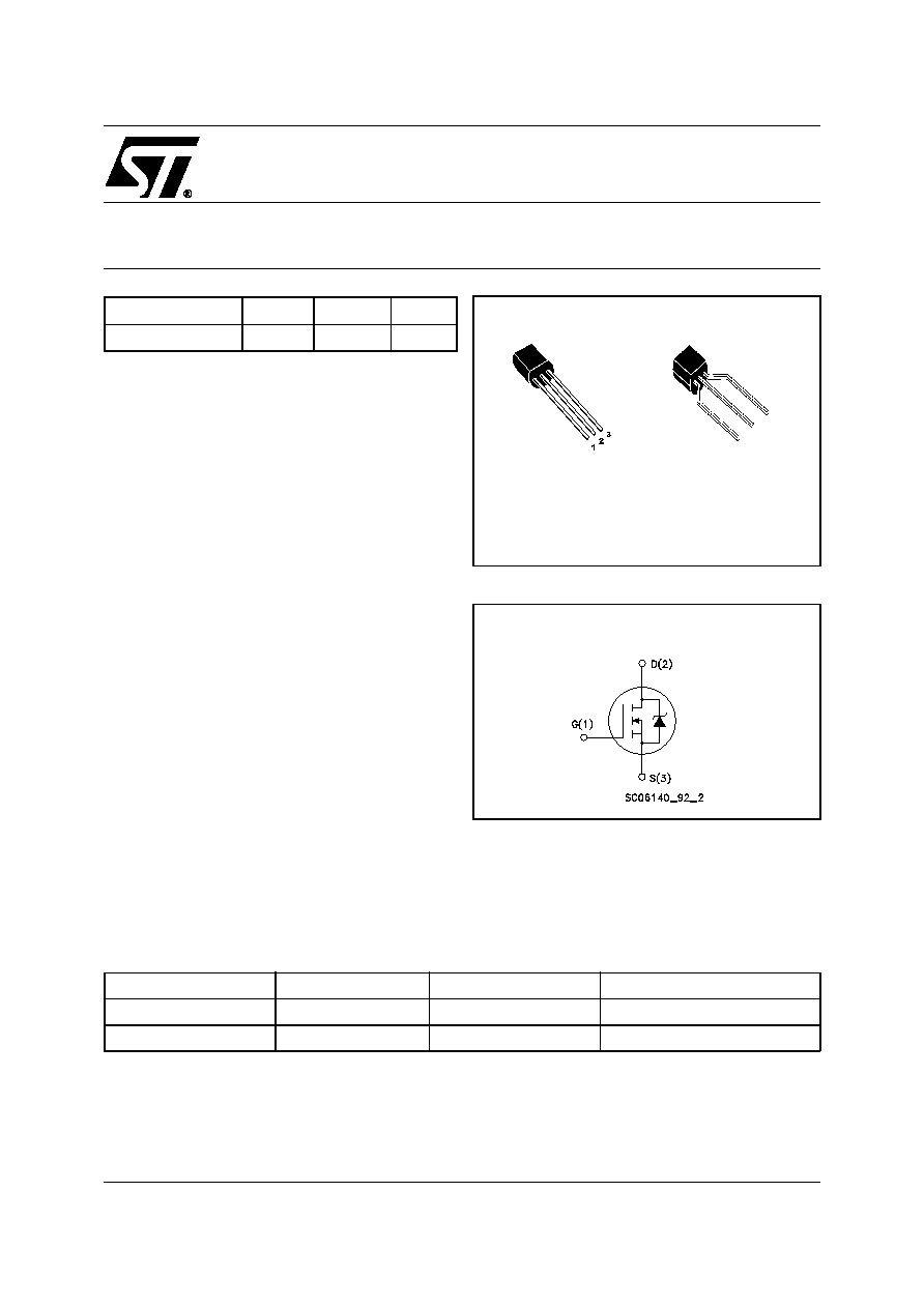
TO-92
TO-92
BULK
(AMMOPACK)
INTERNAL SCHEMATIC DIAGRAM
STQ1NC60R
2/9
ABSOLUTE MAXIMUM RATINGS
( ) Pulse width limited by safe operating area
(1) I
SD
0.3A, di/dt
100A/µs, V
DD
V
(BR)DSS
, T
j
T
JMAX.
THERMAL DATA
AVALANCHE CHARACTERISTICS
ELECTRICAL CHARACTERISTICS (TCASE =25∞C UNLESS OTHERWISE SPECIFIED)
ON/OFF
Symbol
Parameter
Value
Unit
V
DS
Drain-source Voltage (V
GS
= 0)
600
V
V
DGR
Drain-gate Voltage (R
GS
= 20 k
)
600
V
V
GS
Gate- source Voltage
± 30
V
I
D
Drain Current (continuous) at T
C
= 25∞C
0.3
A
I
D
Drain Current (continuous) at T
C
= 100∞C
0.19
A
I
DM
( )
Drain Current (pulsed)
1.2
A
P
TOT
Total Dissipation at T
C
= 25∞C
3.1
W
Derating Factor
0.025
W/∞C
dv/dt (1)
Peak Diode Recovery voltage slope
3
V/ns
T
j
T
stg
Operating Junction Temperature
Storage Temperature
-65 to 150
-65 to 150
∞C
∞C
TO-92
Rthj-amb
Thermal Resistance Junction-ambient Max
120
∞C/W
Rthj-lead
Thermal Resistance Junction-lead Max
40
∞C/W
T
l
Maximum Lead Temperature For Soldering Purpose
260
∞C
Symbol
Parameter
Max Value
Unit
I
AR
Avalanche Current, Repetitive or Not-Repetitive
(pulse width limited by T
j
max)
0.3
A
E
AS
Single Pulse Avalanche Energy
(starting T
j
= 25 ∞C, I
D
= I
AR
, V
DD
= 50 V)
60
mJ
Symbol
Parameter
Test Conditions
Min.
Typ.
Max.
Unit
V
(BR)DSS
Drain-source
Breakdown Voltage
I
D
= 250 µA, V
GS
= 0
600
V
I
DSS
Zero Gate Voltage
Drain Current (V
GS
= 0)
V
DS
= Max Rating
V
DS
= Max Rating, T
C
= 125 ∞C
1
50
µA
µA
I
GSS
Gate-body Leakage
Current (V
DS
= 0)
V
GS
= ± 30V
±100
nA
V
GS(th)
Gate Threshold Voltage
V
DS
= V
GS
, I
D
= 250µA
2
3
4
V
R
DS(on)
Static Drain-source On
Resistance
V
GS
= 10V, I
D
= 0.3 A
12
15
3/9
STQ1NC60R
ELECTRICAL CHARACTERISTICS (TCASE =25∞C UNLESS OTHERWISE SPECIFIED)
DYNAMIC
SWITCHING ON
SWITCHING OFF
SOURCE DRAIN DIODE
Note: 1. Pulsed: Pulse duration = 300 µs, duty cycle 1.5 %.
2. Pulse width limited by safe operating area.
Symbol
Parameter
Test Conditions
Min.
Typ.
Max.
Unit
g
fs
(1)
Forward Transconductance
V
DS
= 15 V
,
I
D
= 0.3 A
0.87
S
C
iss
C
oss
C
rss
Input Capacitance
Output Capacitance
Reverse Transfer
Capacitance
V
DS
= 25V, f = 1 MHz, V
GS
= 0
108
18
2.5
pF
pF
pF
Symbol
Parameter
Test Conditions
Min.
Typ.
Max.
Unit
t
d(on)
t
r
Turn-on Delay Time
Rise Time
V
DD
= 300 V, I
D
= 0.5 A
R
G
= 4.7
V
GS
= 10 V
(Resistive Load see, Figure 3)
7.2
8
ns
ns
Q
g
Q
gs
Q
gd
Total Gate Charge
Gate-Source Charge
Gate-Drain Charge
V
DD
= 480V, I
D
= 1 A,
V
GS
= 10V, R
G
= 4.7
7.3
3.4
2.5
10
nC
nC
nC
Symbol
Parameter
Test Conditions
Min.
Typ.
Max.
Unit
t
r(Voff)
t
f
t
c
Off-voltage Rise Time
Fall Time
Cross-over Time
V
DD
= 480V, I
D
= 1 A,
R
G
= 4.7
,
V
GS
= 10V
(Inductive Load see, Figure 5)
33
11
43
ns
ns
ns
Symbol
Parameter
Test Conditions
Min.
Typ.
Max.
Unit
I
SD
I
SDM
(2)
Source-drain Current
Source-drain Current (pulsed)
0.3
1.2
A
A
V
SD
(1)
Forward On Voltage
I
SD
= 0.3 A, V
GS
= 0
1.6
V
t
rr
Q
rr
I
RRM
Reverse Recovery Time
Reverse Recovery Charge
Reverse Recovery Current
I
SD
= 1 A, di/dt = 100A/µs
V
DD
= 25 V, T
j
= 150∞C
(see test circuit, Figure 5)
450
720
3.2
ns
µ
C
A
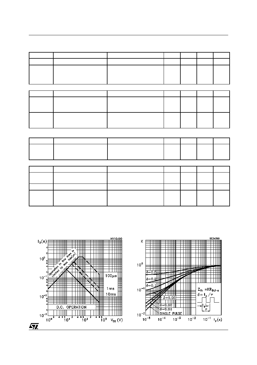
Thermal Impedance
Safe Operating Area
STQ1NC60R
4/9
.
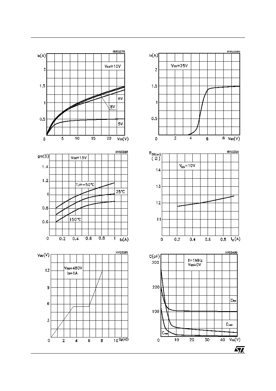
Gate Charge vs Gate-source Voltage
Capacitance Variations
Tranconductance
Output Characteristics
Transfer Characteristics
Static Drain-Source On Resistance
5/9
STQ1NC60R
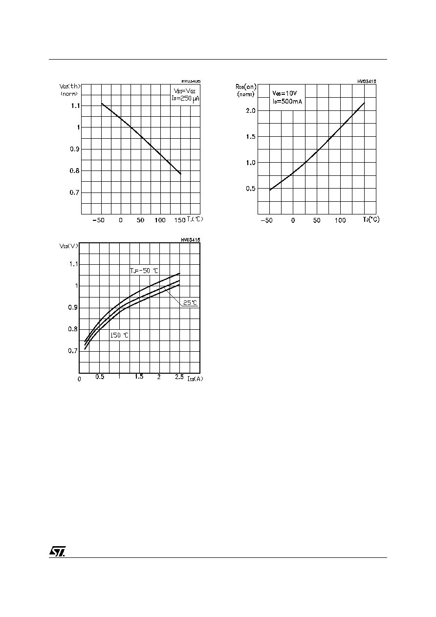
Normalized On Resistance vs Temperature
Normalized Gate Thereshold Voltage vs Temp.
Source-drain Diode Forward Characteristics