1/14
September 2005
STD1LNK60Z-1
STQ1NK60ZR - STN1NK60Z
N-CHANNEL 600V 13
0.8A TO-92/IPAK/SOT-223
Zener-Protected SuperMESHTMMOSFET
Table 1: General Features
TYPICAL R
DS
(on) = 13
EXTREMELY HIGH dv/dt CAPABILITY
ESD IMPROVED CAPABILITY
100% AVALANCHE TESTED
NEW HIGH VOLTAGE BENCHMARK
GATE CHARGE MINIMIZED
DESCRIPTION
The SuperMESHTM series is obtained through an
extreme optimization of ST's well established
strip-based PowerMESHTM layout. In addition to
pushing on-resistance significantly down, special
care is taken to ensure a very good dv/dt capability
for the most demanding applications. Such series
complements ST full range of high voltage MOS-
FETs including revolutionary MDmeshTM products.
APPLICATIONS
AC ADAPTORS AND BATTERY CHARGERS
SWITH MODE POWER SUPPLIES (SMPS)
Table 2: Order Codes
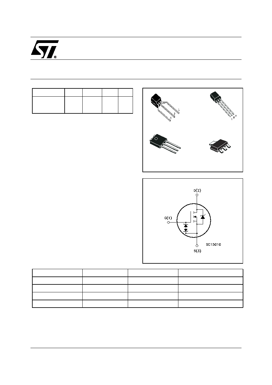
Figure 1: Package
Figure 2: Internal Schematic Diagram
TYPE
V
DSS
R
DS(on)
I
D
Pw
STQ1NK60ZR
STD1LNK60Z-1
STN1NK60Z
600 V
600 V
600 V
< 15
< 15
< 15
0.3 A
0.8 A
0.3 A
3 W
25 W
3.3 W
TO-92
3
2
1
IPAK
TO-92 (Ammopack)
1
2
2
3
SOT-223
SALES TYPE
MARKING
PACKAGE
PACKAGING
STQ1NK60ZR
Q1NK60ZR
TO-92
BULK
STQ1NK60ZR-AP
Q1NK60ZR
TO-92
AMMOPAK
STD1LNK60Z-1
D1LNK60Z
IPAK
TUBE
STN1NK60Z
N1NK60Z
SOT-223
TAPE & REEL
Rev. 6
STD1LNK60Z-1 - STQ1NK60ZR - STN1NK60Z
2/14
Table 3: Absolute Maximum ratings
( ) Pulse width limited by safe operating area
(1) I
SD
0.3A, di/dt
200A/µs, V
DD
V
(BR)DSS
, T
j
T
JMAX.
Table 4: Thermal Data
(#) When mounted on 1 inch≤ Fr-4 board, 2 Oz Cu
Table 5: Avalanche Characteristics
Table 6: Gate-Source Zener Diode
PROTECTION FEATURES OF GATE-TO-SOURCE ZENER DIODES
The built-in back-to-back Zener diodes have specifically been designed to enhance not only the device's
ESD capability, but also to make them safely absorb possible voltage transients that may occasionally be
applied from gate to source. In this respect the Zener voltage is appropriate to achieve an efficient and
cost-effective intervention to protect the device's integrity. These integrated Zener diodes thus avoid the
usage of external components.
Symbol
Parameter
Value
Unit
IPAK
TO-92
SOT-223
V
DS
Drain-source Voltage (V
GS
= 0)
600
V
V
DGR
Drain-gate Voltage (R
GS
= 20 k
)
600
V
V
GS
Gate- source Voltage
± 30
V
I
D
Drain Current (continuous) at T
C
= 25∞C
0.8
0.3
0.3
A
I
D
Drain Current (continuous) at T
C
= 100∞C
0.5
0.189
0.189
A
I
DM
( )
Drain Current (pulsed)
3.2
1.2
1.2
A
P
TOT
Total Dissipation at T
C
= 25∞C
25
3
3.3
W
Derating Factor
0.24
0.025
0.026
W/∞C
V
ESD(G-S)
Gate source ESD(HBM-C=100pF, R=1.5K
)
800
V
dv/dt (1)
Peak Diode Recovery voltage slope
4.5
V/ns
T
j
T
stg
Operating Junction Temperature
Storage Temperature
-55 to 150
∞C
IPAK
TO-92
SOT-223
Rthj-case
Thermal Resistance Junction-case Max
5
--
--
∞C/W
Rthj-amb
Thermal Resistance Junction-ambient Max
100
120
37.87(#)
∞C/W
Rthj-lead
Thermal Resistance Junction-lead Max
--
40
--
∞C/W
T
l
Maximum Lead Temperature For Soldering Purpose
275
260
260
∞C
Symbol
Parameter
Max Value
Unit
I
AR
Avalanche Current, Repetitive or Not-Repetitive
(pulse width limited by T
j
max)
0.8
A
E
AS
Single Pulse Avalanche Energy
(starting T
j
= 25 ∞C, I
D
= I
AR
, V
DD
= 50 V)
60
mJ
Symbol
Parameter
Test Conditions
Min.
Typ.
Max.
Unit
BV
GSO
Gate-Source Breakdown
Voltage
Igs=± 1mA (Open Drain)
30
V
3/14
STD1LNK60Z-1 - STQ1NK60ZR - STN1NK60Z
ELECTRICAL CHARACTERISTICS (T
CASE
=25∞C UNLESS OTHERWISE SPECIFIED)
Table 7: On /Off
Table 8: Dynamic
Table 9: Source Drain Diode
Note: 1. Pulsed: Pulse duration = 300 µs, duty cycle 1.5 %.
2. Pulse width limited by safe operating area.
3. C
oss eq.
is defined as a constant equivalent capacitance giving the same charging time as C
oss
when V
DS
increases from 0 to 80%
V
DSS
.
Symbol
Parameter
Test Conditions
Min.
Typ.
Max.
Unit
V
(BR)DSS
Drain-source
Breakdown Voltage
I
D
= 1 mA, V
GS
= 0
600
V
I
DSS
Zero Gate Voltage
Drain Current (V
GS
= 0)
V
DS
= Max Rating
V
DS
= Max Rating,
T
C
= 125 ∞C
1
50
µA
µA
I
GSS
Gate-body Leakage
Current (V
DS
= 0)
V
GS
= ± 20V
±10
µA
V
GS(th)
Gate Threshold Voltage
V
DS
= V
GS
, I
D
= 50 µA
3
3.75
4.5
V
R
DS(on)
Static Drain-source On
Resistance
V
GS
= 10V, I
D
= 0.4 A
13
15
Symbol
Parameter
Test Conditions
Min.
Typ.
Max.
Unit
g
fs
(1)
Forward Transconductance
V
DS
= V
,
I
D
= 0.4 A
0.5
S
C
iss
C
oss
C
rss
Input Capacitance
Output Capacitance
Reverse Transfer
Capacitance
V
DS
= 25V, f = 1 MHz, V
GS
= 0
94
17.6
2.8
pF
pF
pF
C
oss eq.
(3)
Equivalent Output
Capacitance
V
GS
= 0V, V
DS
= 0V to 480V
11
pF
t
d(on)
t
r
t
d(off)
t
f
Turn-on Delay Time
Rise Time
Turn-off-Delay Time
Fall Time
V
DD
= 300V, I
D
= 0.4 A
R
G
= 4.7
V
GS
= 10 V
(see Figure 21)
5.5
5
13
28
ns
ns
ns
ns
Q
g
Q
gs
Q
gd
Total Gate Charge
Gate-Source Charge
Gate-Drain Charge
V
DD
= 480V, I
D
= 0.8 A,
V
GS
= 10V
(see Figure 25)
4.9
1
2.7
6.9
nC
nC
nC
Symbol
Parameter
Test Conditions
Min.
Typ.
Max.
Unit
I
SD
I
SDM
(2)
Source-drain Current
Source-drain Current (pulsed)
0.8
2.4
A
A
V
SD
(1)
Forward On Voltage
I
SD
= 0.8A, V
GS
= 0
1.6
V
t
rr
Q
rr
I
RRM
Reverse Recovery Time
Reverse Recovery Charge
Reverse Recovery Current
I
SD
= 0.8 A, di/dt = 100A/µs
V
DD
= 20V, T
j
= 25∞C
(see Figure 23)
135
216
3.2
ns
nC
A
t
rr
Q
rr
I
RRM
Reverse Recovery Time
Reverse Recovery Charge
Reverse Recovery Current
I
SD
= 0.8 A, di/dt = 100A/µs
V
DD
= 20V, T
j
= 150∞C
(see Figure 23)
140
224
3.2
ns
nC
A
STD1LNK60Z-1 - STQ1NK60ZR - STN1NK60Z
4/14
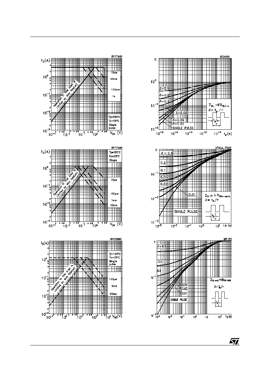
Figure 3: Safe Operating Area for IPAK
Figure 4: Safe Operating Area for TO-92
Figure 5: Safe Operating Area for SOT-223
Figure 6: Thermal Impedance for IPAK
Figure 7: Thermal Impedance for TO-92
Figure 8: Thermal Impedance for SOT-223
5/14
STD1LNK60Z-1 - STQ1NK60ZR - STN1NK60Z
Figure 9: Output Characteristics
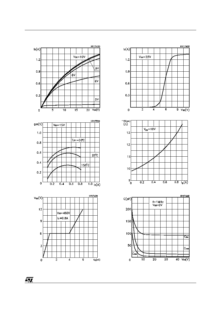
Figure 10: Transconductance
Figure 11: Gate Charge vs Gate-source Voltage
Figure 12: Transfer Characteristics
Figure 13: Statis Drain-Source On Resistance
Figure 14: Capacitance Variation