 | –≠–ª–µ–∫—Ç—Ä–æ–Ω–Ω—ã–π –∫–æ–º–ø–æ–Ω–µ–Ω—Ç: STS15N4LL | –°–∫–∞—á–∞—Ç—å:  PDF PDF  ZIP ZIP |
June 2006
Rev 1
1/12
12
STS15N4LL
N-channel 40V - 0.0042
- 15A - SO-8
STripFETTM Power MOSFET
Optimal R
DS(on)
x Q
g
trade-off @ 4.5V
Conduction losses reduced
Switching losses reduced
Description
This N-channel enhancement mode Power
MOSFET is the latest refinement of
STMicroelectronic unique "Single Feature SizeTM"
strip-based process with less critical aligment
steps and therefore a remarkable manufacturing
reproducibility. The resulting transistor shows
extremely high packing density for low on-
resistance, rugged avalanche characteristics and
low gate charge.
Applications
Switching application
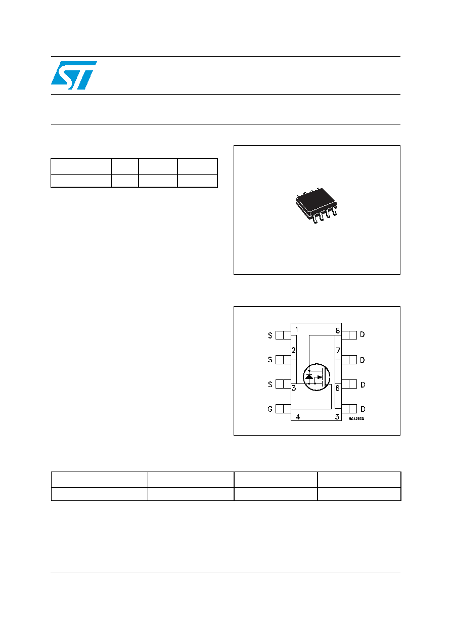
Internal schematic diagram
General features
Type
V
DSS
R
DS(on)
I
D
STS15N4LL
40V
<0.005
15A
SO-8
www.st.com
Order codes
Part number
Marking
Package
Packaging
STS15N4LL
15N4LL-
SO-8
Tape & reel

Contents
STS15N4LL
2/12
Contents
1
Electrical ratings . . . . . . . . . . . . . . . . . . . . . . . . . . . . . . . . . . . . . . . . . . . . 3
2
Electrical characteristics . . . . . . . . . . . . . . . . . . . . . . . . . . . . . . . . . . . . . 4
2.1
Electrical characteristics (curves) . . . . . . . . . . . . . . . . . . . . . . . . . . . . . 6
3
Test circuit . . . . . . . . . . . . . . . . . . . . . . . . . . . . . . . . . . . . . . . . . . . . . . . . 8
4
Package mechanical data . . . . . . . . . . . . . . . . . . . . . . . . . . . . . . . . . . . . . 9
5
Revision history . . . . . . . . . . . . . . . . . . . . . . . . . . . . . . . . . . . . . . . . . . 11
STS15N4LL
Electrical ratings
3/12
1 Electrical
ratings
Table 1.
Absolute maximim ratings
Symbol
Parameter
Value
Unit
V
DS
Drain-source voltage (V
GS
= 0)
40
V
V
GS
Gate-source voltage
± 16
V
V
GS
(1)
1.
Guaranteed for test time < 15ms
Gate- source voltage
±18
V
I
D
Drain current (continuous) at T
C
= 25∞C
15
A
I
D
Drain current (continuous) at T
C
= 100∞C
9.3
A
I
DM
(2)
2.
Pulse width limited by Tjmax
Drain current (pulsed)
60
A
P
TOT
Total dissipation at T
C
= 25∞C
2.7
W
E
AS
(3)
3.
Starting T
j
=25∞C, I
D
=7.5A, V
DD
=25V
Single pulse avalanche energy
2
J
Table 2.
Thermal resistance
Symbol
Parameter
Value
Unit
R
thj
-pcb
(1)
1.
When mounted of FR-4 board with 1 inch
2
pad, 2oz of Cu and t< 10sec
Thermal resistance junction-PCB Max
47
∞C/W
T
l
Maximum lead temperature for soldering
-55 to 150
∞C
T
stg
Storage temperature
-55 to 150
∞C
Electrical characteristics
STS15N4LL
4/12
2 Electrical
characteristics
(T
J
= 25 ∞C unless otherwise specified)
Table 3.
On/off states
Symbol
Parameter
Test conditions
Min.
Typ.
Max.
Unit
V
(BR)DSS
Drain-source breakdown
voltage
I
D
= 250µA, V
GS
= 0
40
V
I
DSS
Zero gate voltage drain
current (V
GS
= 0)
V
DS
= max rating,
V
DS
=max rating @125∞C
10
100
µA
µA
I
GSS
Gate body leakage
Current (V
DS
= 0)
V
GS
= ±16V
±
200
nA
V
GS(th)
Gate threshold voltage
V
DS
= V
GS
, I
D
= 250µA
1
V
R
DS(on)
Static drain-source On
resistance
V
GS
= 10V, I
D
= 7.5A
V
GS
= 4.5V, I
D
= 7.5A
0.0042
0.005
0.005
0.007
Table 4.
Dynamic
Symbol
Parameter
Test conditions
Min.
Typ.
Max.
Unit
C
iss
C
oss
C
rss
Input capacitance
Output capacitance
Reverse transfer
Capacitance
V
DS
= 25V, f=1 MHz,
V
GS
= 0
2530
574
29
pF
pF
pF
Q
g
Q
gs
Q
gd
Total gate charge
Gate-source charge
Gate-drain charge
V
DD
= 20V, I
D
= 15A
V
GS
= 4.5V
(see Figure 13)
21.5
6.9
8.2
28
nC
nC
nC
R
G
Gate input resistance
f=1 MHz Gate DC Bias = 0
Test signal level = 20mV
open drain
1
3
5
Table 5.
Switching times
Symbol
Parameter
Test conditions
Min.
Typ.
Max.
Unit
t
d(on)
t
r
Turn-on delay time
Rise time
V
DD
= 20V, I
D
= 7.5A,
R
G
= 4.7
, V
GS
= 10V
(see Figure 12)
17
25
ns
ns
t
d(off)
t
f
Turn-off delay time
Fall time
V
DD
= 20V, I
D
= 7.5A,
R
G
= 4.7
, V
GS
= 10V
(see Figure 12)
62
9
ns
ns
STS15N4LL
Electrical characteristics
5/12
Table 6.
Source drain diode
Symbol
Parameter
Test conditions
Min.
Typ.
Max.
Unit
I
SD
I
SDM
(1)
1.
Pulse width limited by safe operating area
Source-drain current
Source-drain current (pulsed)
15
60
A
A
V
SD
(2)
2.
Pulsed: pulse duration = 300µs, duty cycle 1.5%
Forward on voltage
I
SD
= 15A, V
GS
= 0
1.2
V
t
rr
Q
rr
I
RRM
Reverse recovery time
Reverse recovery charge
Reverse recovery current
I
SD
= 15A, V
DD
= 30V,
di/dt = 100A/µs,
Tj = 150∞C
(see Figure 17)
43
64
3
ns
nC
A