1/6
PRELIMINARY DATA
August 2001
STS2DPF20V
DUAL P-CHANNEL 20V - 0.14
- 2A SO-8
2.7V-DRIVE STripFETTM II POWER MOSFET
Note: For the P-CHANNEL MOSFET actual polarity of Voltages
and current has to be reversed
s
TYPICAL R
DS
(on) = 0.14
(@4.5V)
s
TYPICAL R
DS
(on) = 0.2
(@2.7V)
s
ULTRA LOW THRESHOLD GATE DRIVE (2.7V)
s
STANDARD OUTLINE FOR EASY
AUTOMATED SURFACE MOUNT ASSEMBLY
DESCRIPTION
This Power MOSFET is the second generation of
STMicroelectronics unique "Single Feature SizeTM"
strip-based process. The resulting transistor shows
extremely high packing density for low on-
resistance, rugged avalanche characteristics and
less critical alignment steps therefore a remarkable
manufacturing reproducibility.
APPLICATIONS
s
BATTERY MANAGMENT IN NOMADIC
EQUIPMENT
s
POWER MANAGMENT IN CELLULAR PHONES
MOSFET ABSOLUTE MAXIMUM RATINGS
(
q
)Pulse width limited by safe operating area
.
TYPE
V
DSS
R
DS(on)
I
D
STS2DPF20V
20 V
<0.20
(@4.5V)
<0.25
(@2.7V)
2 A
Symbol
Parameter
Value
Unit
V
DS
Drain-source Voltage (V
GS
= 0)
20
V
V
DGR
Drain-gate Voltage (R
GS
= 20 k
)
20
V
V
GS
Gate- source Voltage
� 12
V
I
D
Drain Current (continuos) at T
C
= 25�C Single Operation
Drain Current (continuos) at T
C
= 100�C Single Operation
2
1.26
A
A
I
DM
(
q
)
Drain Current (pulsed)
8
A
P
TOT
Total Dissipation at T
C
= 25�C Dual Operation
Total Dissipation at T
C
= 25�C Single Operation
1.6
2
W
W
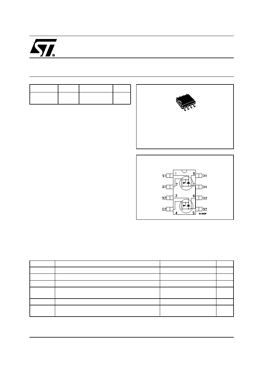
SO-8
INTERNAL SCHEMATIC DIAGRAM

STS2DPF20V
2/6
THERMAL DATA
MOSFET ELECTRICAL CHARACTERISTICS (TCASE = 25 �C UNLESS OTHERWISE SPECIFIED)
OFF
ON (1)
DYNAMIC
Rthj-amb
(*)Thermal Resistance Junction-ambient Single Operation
Dual Operation
62.5
78
�C/W
�C/W
T
stg
Storage Temperature
-55 to 150
�C
T
j
Junction-ambient Temperature
-55 to 150
�C
(*) When Mounted on 0.5 in
�
of 2 oz. Copper
Symbol
Parameter
Test Conditions
Min.
Typ.
Max.
Unit
V
(BR)DSS
Drain-source
Breakdown Voltage
I
D
= 250 �A, V
GS
= 0
20
V
I
DSS
Zero Gate Voltage
Drain Current (V
GS
= 0)
V
DS
= Max Rating
1
�A
V
DS
= Max Rating, T
C
= 125 �C
10
�A
I
GSS
Gate-body Leakage
Current (V
DS
= 0)
V
GS
= � 12 V
�100
nA
Symbol
Parameter
Test Conditions
Min.
Typ.
Max.
Unit
V
GS(th)
Gate Threshold Voltage
V
DS
= V
GS
, I
D
= 250�A
0.6
V
R
DS(on)
Static Drain-source On
Resistance
V
GS
= 4.5 V, I
D
= 1 A
0.14
0.20
V
GS
= 2.7 V, I
D
= 1 A
0.20
0.25
Symbol
Parameter
Test Conditions
Min.
Typ.
Max.
Unit
g
fs
(1)
Forward Transconductance
V
DS
= 15 V
,
I
D
= 1.5 A
4.5
S
C
iss
Input Capacitance
V
DS
= 15V, f = 1 MHz, V
GS
= 0
315
pF
C
oss
Output Capacitance
87
pF
C
rss
Reverse Transfer
Capacitance
17
pF
3/6
STS2DPF20V
ELECTRICAL CHARACTERISTICS (CONTINUED)
SWITCHING ON
SWITCHING OFF
SOURCE DRAIN DIODE
Note: 1. Pulsed: Pulse duration = 300 �s, duty cycle 1.5 %.
2. Pulse width limited by safe operating area.
Symbol
Parameter
Test Conditions
Min.
Typ.
Max.
Unit
t
d(on)
Turn-on Delay Time
V
DD
= 10 V, I
D
= 1.5A
R
G
= 4.7
V
GS
= 4.5V
(see test circuit, Figure 1)
38
ns
t
r
Rise Time
30
ns
Q
g
Total Gate Charge
V
DD
= 10V, I
D
= 2 A,
V
GS
= 4.5 V
(see test circuit, Figure 2)
3.8
4.8
nC
Q
gs
Gate-Source Charge
0.34
nC
Q
gd
Gate-Drain Charge
0.8
nC
Symbol
Parameter
Test Conditions
Min.
Typ.
Max.
Unit
t
d(off)
t
f
Turn-off Delay Time
Fall Time
V
DD
= 10 V, I
D
= 1 A,
R
G
= 4.7
,
V
GS
= 4.5 V
(see test circuit, Figure 1)
45
11
ns
ns
Symbol
Parameter
Test Conditions
Min.
Typ.
Max.
Unit
I
SD
Source-drain Current
2
A
I
SDM
(2)
Source-drain Current (pulsed)
8
A
V
SD
(1)
Forward On Voltage
I
SD
= 2 A, V
GS
= 0
1.2
V
t
rr
Reverse Recovery Time
I
SD
= 2 A, di/dt = 100A/�s,
V
DD
= 10 V, T
j
= 150�C
(see test circuit, Figure 3)
15
ns
Q
rr
Reverse Recovery Charge
7.5
nC
I
RRM
Reverse Recovery Current
1
A
STS2DPF20V
4/6
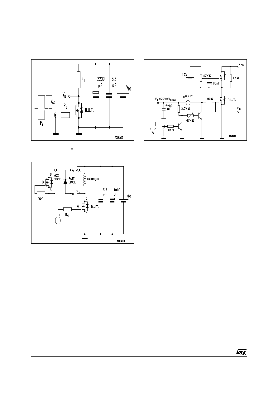
Fig. 3: Test Circuit For Diode Recovery Behaviour
Fig. 2: Gate Charge test Circuit
Fig. 1: Switching Times Test Circuit For
Resistive Load
5/6
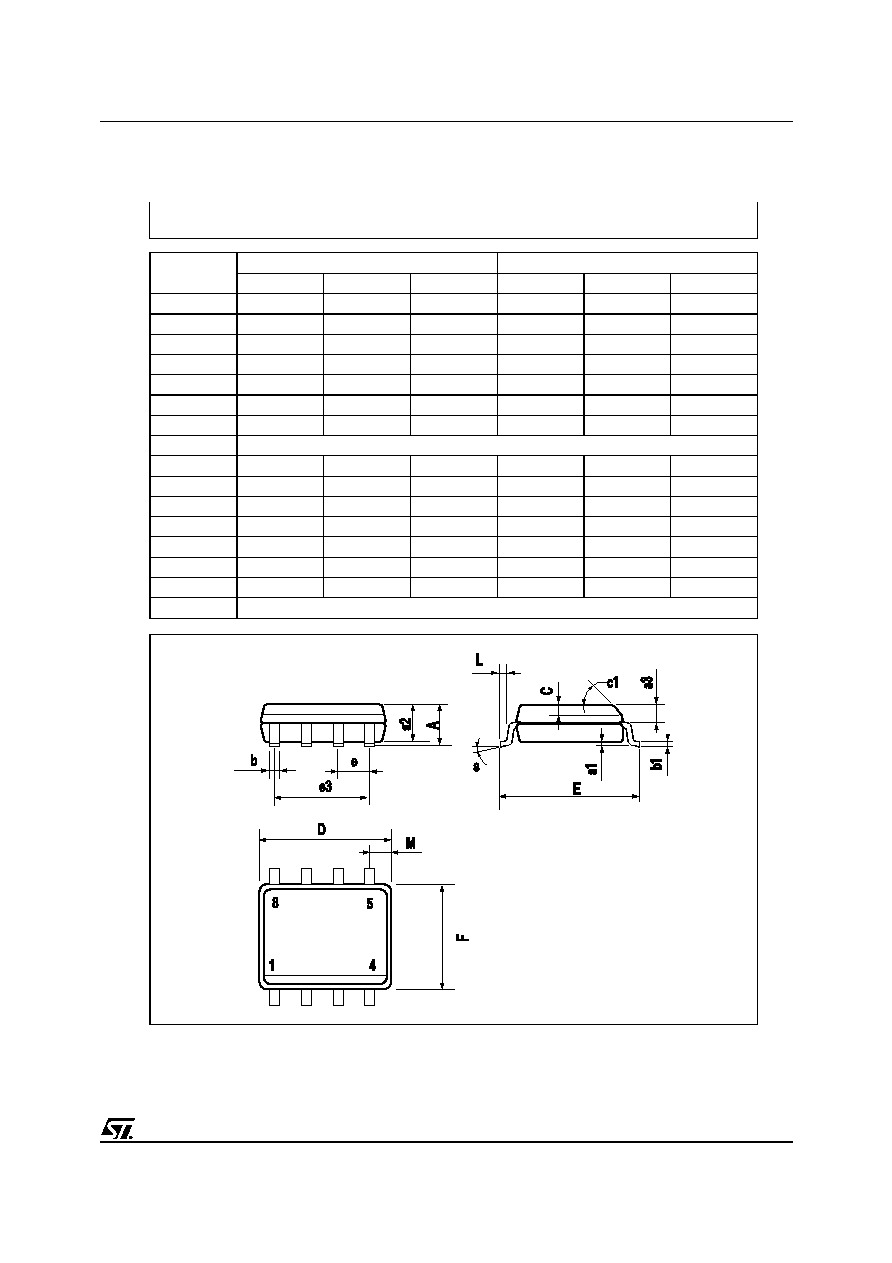
STS2DPF20V
DIM.
mm
inch
MIN.
TYP.
MAX.
MIN.
TYP.
MAX.
A
1.75
0.068
a1
0.1
0.25
0.003
0.009
a2
1.65
0.064
a3
0.65
0.85
0.025
0.033
b
0.35
0.48
0.013
0.018
b1
0.19
0.25
0.007
0.010
C
0.25
0.5
0.010
0.019
c1
45 (typ.)
D
4.8
5.0
0.188
0.196
E
5.8
6.2
0.228
0.244
e
1.27
0.050
e3
3.81
0.150
F
3.8
4.0
0.14
0.157
L
0.4
1.27
0.015
0.050
M
0.6
0.023
S
8 (max.)
0016023
SO-8 MECHANICAL DATA