 | –≠–ª–µ–∫—Ç—Ä–æ–Ω–Ω—ã–π –∫–æ–º–ø–æ–Ω–µ–Ω—Ç: STS2DPF80 | –°–∫–∞—á–∞—Ç—å:  PDF PDF  ZIP ZIP |
1/9
June 2004
STS2DPF80
DUAL P-CHANNEL 80V - 0.21
- 2.3A SO-8
STripFETTM POWER MOSFET
Rev.0.1
TYPICAL R
DS
(on) = 0.21
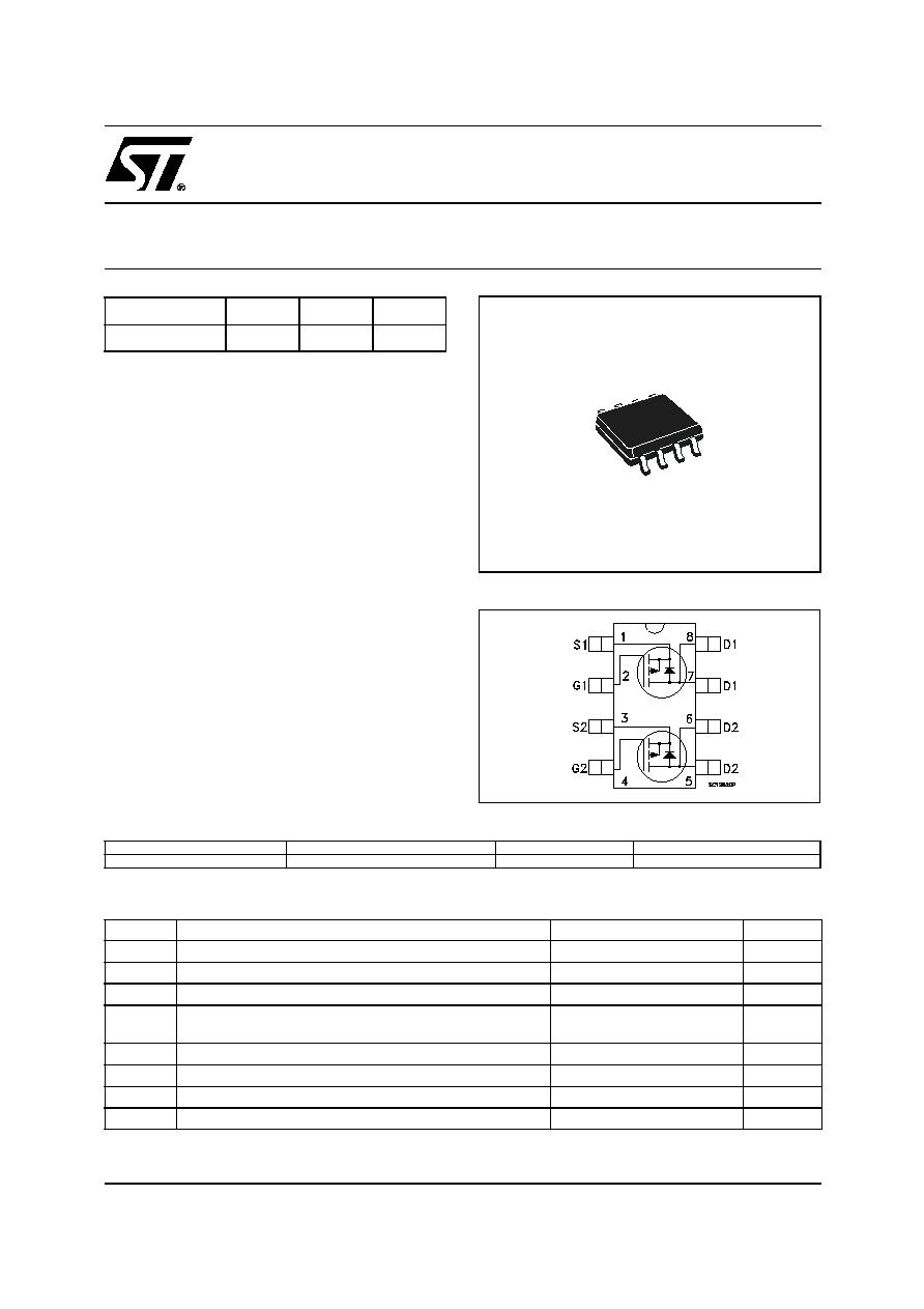
STANDARD OUTLINE FOR EASY
AUTOMATED SURFACE MOUNT ASSEMBLY
DESCRIPTION
This application specific Power MOSFET is the
second generation of STMicroelectronis unique
"Single Feature SizeTM" strip-based process. The
resulting transistor shows extremely high packing
density for low on-resistance, rugged avalanche
characteristics and less critical alignment steps
therefore a remarkable manufacturing reproduc-
ibility
.
APPLICATIONS
DC/DC CONVERTERS
BATTERY MANAGEMENT IN NOMADIC
EQUIPMENT
POWER MANAGEMENT IN CELLULAR
PHONES AND DISPLAY NEW GENERATION
Ordering Information
TYPE
V
DSS
R
DS(on)
I
D
STS2DPF80
80 V
<0.25
2.3 A
SALES TYPE
MARKING
PACKAGE
PACKAGING
STS8DPF80
S8DPF80
SO-8
TAPE & REEL
SO-8
ABSOLUTE MAXIMUM RATINGS
(
∑)
Pulse width limited by safe operating area.
Note: For the P-CHANNEL MOSFET actual polarity of voltages and
current has to be reversed
Symbol
Parameter
Value
Unit
V
DS
Drain-source Voltage (V
GS
= 0)
80
V
V
DGR
Drain-gate Voltage (R
GS
= 20 k
)
80
V
V
GS
Gate- source Voltage
± 20
V
I
D
Drain Current (continuous) at T
C
= 25∞C Single Operation
Drain Current (continuous) at T
C
= 100∞C Single Operation
2.0
1.3
A
A
I
DM
(
∑)
Drain Current (pulsed)
8
A
P
tot
Total Dissipation at T
C
= 25∞C
2.5
W
T
stg
Storage Temperature
-55 to 150
∞C
T
j
Max. Operating Junction Temperature
150
∞C
INTERNAL SCHEMATIC DIAGRAM
STS2DPF80
2/9
TAB.1 THERMAL DATA
(*)
When Mounted on 1 inch
2
FR-4 board, 2 oz of Cu and t
[
10 sec.
ELECTRICAL CHARACTERISTICS (T
CASE
= 25 ∞C UNLESS OTHERWISE SPECIFIED)
TAB.2 OFF
TAB.3 ON
(*)
TAB.4 DYNAMIC
Rthj-
PCB(*)
Thermal Resistance Junction-PCB
62.5
∞C/W
Symbol
Parameter
Test Conditions
Min.
Typ.
Max.
Unit
V
(BR)DSS
Drain-source
Breakdown Voltage
I
D
= 250 µA, V
GS
= 0
80
V
I
DSS
Zero Gate Voltage
Drain Current (V
GS
= 0)
V
DS
= Max Rating
V
DS
= Max Rating T
C
= 125∞C
1
10
µA
µA
I
GSS
Gate-body Leakage
Current (V
DS
= 0)
V
GS
= ± 20 V
±100
nA
Symbol
Parameter
Test Conditions
Min.
Typ.
Max.
Unit
V
GS(th)
Gate Threshold Voltage
V
DS
= V
GS
I
D
= 250 µA
2
4
V
R
DS(on)
Static Drain-source On
Resistance
V
GS
= 10 V
I
D
= 1 A
0.21
0.25
Symbol
Parameter
Test Conditions
Min.
Typ.
Max.
Unit
g
fs (*)
Forward Transconductance
V
DS
= 10V
I
D
= 1 A
4
S
C
iss
C
oss
C
rss
Input Capacitance
Output Capacitance
Reverse Transfer
Capacitance
V
DS
= 25V, f = 1 MHz, V
GS
= 0
739
89.5
31
pF
pF
pF

3/9
STS2DPF80
TAB.5 SWITCHING ON
TAB.6 SWITCHING OFF
TAB.7 SOURCE DRAIN DIODE
(*)
Pulsed: Pulse duration = 300 µs, duty cycle 1.5 %.
(
∑
)
Pulse width limited by safe operating area.
Symbol
Parameter
Test Conditions
Min.
Typ.
Max.
Unit
t
d(on)
t
r
Turn-on Delay Time
Rise Time
V
DD
= 40 V
I
D
= 1 A
R
G
= 4.7
V
GS
= 10 V
(Resistive Load, Figure 1)
13.5
18
ns
ns
Q
g
Q
gs
Q
gd
Total Gate Charge
Gate-Source Charge
Gate-Drain Charge
V
DD
= 64V I
D
= 2A V
GS
=10V
(See test circuit, Figure 2)
20
2.5
4.9
nC
nC
nC
Symbol
Parameter
Test Conditions
Min.
Typ.
Max.
Unit
t
d(off)
t
f
Turn-off Delay Time
Fall Time
V
DD
= 40 V
I
D
= 1 A
R
G
= 4.7
,
V
GS
= 10 V
(Resistive Load, Figure 1)
32
13
ns
ns
Symbol
Parameter
Test Conditions
Min.
Typ.
Max.
Unit
I
SD
I
SDM
(
∑
)
Source-drain Current
Source-drain Current (pulsed)
2.3
9.2
A
A
V
SD
(*)
Forward On Voltage
I
SD
= 1 A
V
GS
= 0
1.2
V
t
rr
Q
rr
I
RRM
Reverse Recovery Time
Reverse Recovery Charge
Reverse Recovery Current
I
SD
= 2 A
di/dt = 100A/µs
V
DD
= 40 V
T
j
= 150∞C
(See test circuit, Figure 3)
47
87
3.7
ns
nC
A
ELECTRICAL CHARACTERISTICS (continued)
Safe Operating Area
Thermal Impedance
STS2DPF80
4/9
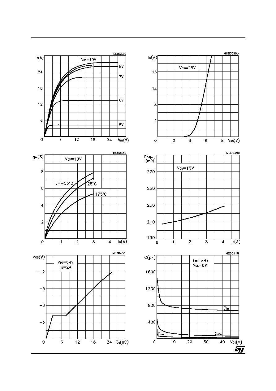
Output Characteristics
Transfer Characteristics
Transconductance
Static Drain-source On Resistance
Gate Charge vs Gate-source Voltage
Capacitance Variations
5/9
STS2DPF80
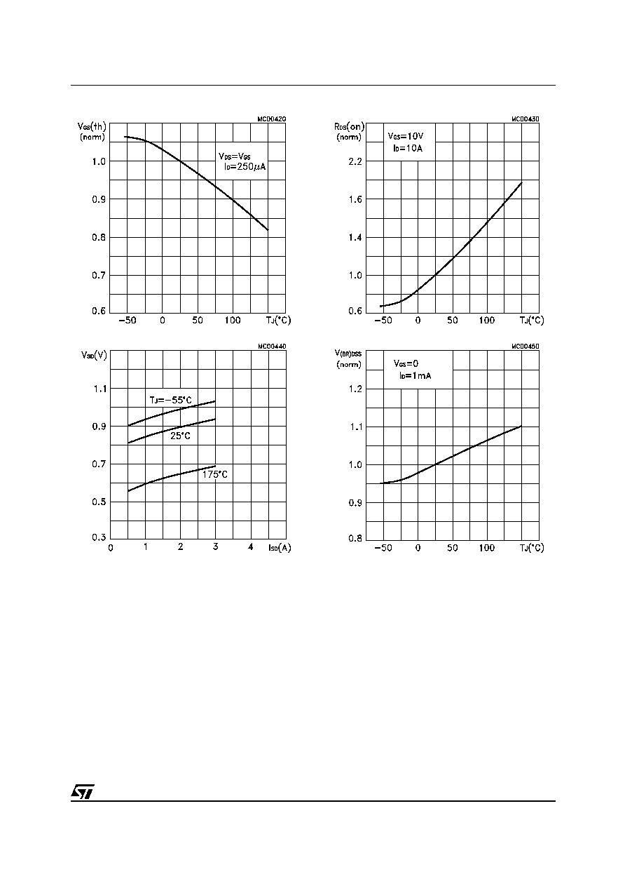
Normalized Gate Threshold Voltage vs Temperature
Normalized
on Resistance vs Temperature
Source-drain Diode Forward Characteristics
Normalized Breakdown Voltage Temperature
.
.
.