STS3DPFS30L
P - CHANNEL 30V - 0.13
- 3A S0-8
STripFET
TM
MOSFET PLUS SCHOTTKY RECTIFIER
PRELIMINARY DATA
DESCRIPTION:
This product associates the latest low voltage
StripFET
TM
in p-channel version to a low drop
Schottky diode. Such configuration is extremely
versatile in implementing, a large variety of DC-DC
converters for printers, portable equipment, and
cellular phones.
Æ
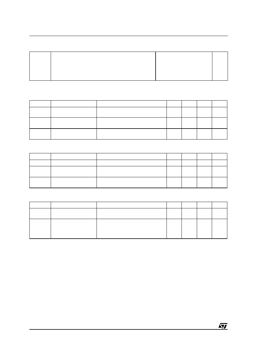
INTERNAL SCHEMATIC DIAGRAM
May 2000
MOSFET ABSOLUTE MAXIMUM RATINGS
Symbol
Parameter
Value
Unit
V
DS
Drain-source Voltage (V
GS
= 0)
30
V
V
DGR
Drain- gate Voltage (R
GS
= 20 k
)
30
V
V
GS
Gate-source Voltage
±
20
V
I
D
Drain Current (continuous) at T
c
= 25
o
C
3
A
I
D
Drain Current (continuous) at T
c
= 100
o
C
1.9
A
I
DM
(
∑
)
Drain Current (pulsed)
12
A
P
tot
Total Dissipation at T
c
= 25
o
C
2
W
MAIN PRODUCT CHARACTERISTICS
MOSFET
V
DSS
R
DS(on)
I
D
30V
<0.16
3A
SCHOTTKY
I
F(AV)
V
RRM
V
F(MAX)
3A
30V
0.51V
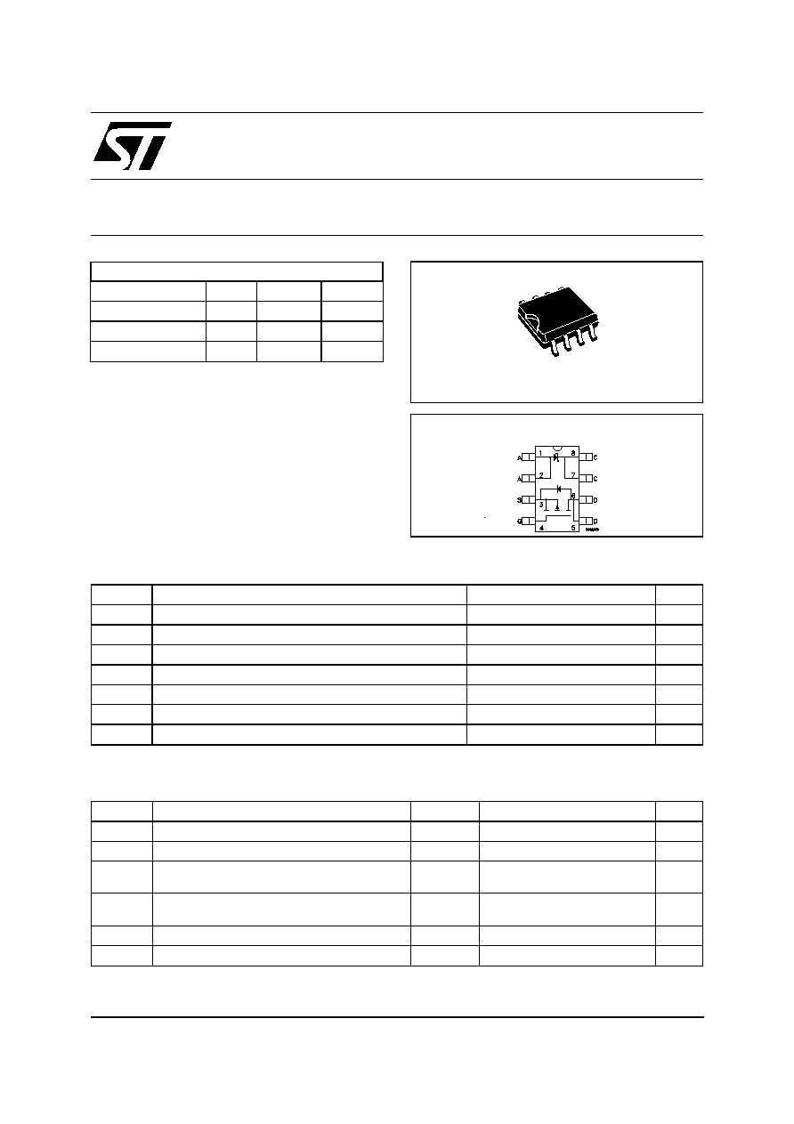
SO-8
SCHOTTKY ABSOLUTE MAXIMUM RATINGS
Symbol
Parameter
Value
Unit
V
RRM
Repetitive Peak Reverse Voltage
30
V
I
F(RMS)
RMS Forward Current
20
A
I
F(AV)
Average Forward Current
T
L
=125
o
C
=0.5
3
A
I
FSM
Surge Non Repetitive Forward Current
tp= 10 ms
Sinusoidal
75
A
I
RSM
Non Repetitive Peak Reverse Current
tp=100
µ
s
1
A
dv/dt
Critical Rate Of Rise Of Reverse Voltage
10000
V/
µ
s
(
∑
) Pulse width limited by safe operating area
Note: For the P-CHANNEL MOSFET actual polarity of voltages and current has to be reversed
1/5
THERMAL DATA
R
thj-amb
R
thj-amb
T
stg
T
j
(*)Thermal Resistance Junction-ambient MOSFET S.O.
Dual Operating
(*) Thermal Resistance Junction-ambientSCHOTTKY
Storage Temperature Range Maximum
Junction Temperature
(*)
mounte d on FR-4 board (ste ady state )
78
62
100
-65 to 150
150
o
C/W
o
C/W
o
C/W
o
C
o
C
MOSFET ELECTRICAL CHARACTERISTICS (T
case
= 25
o
C unless otherwise specified)
OFF
Symbol
Parameter
Test Conditions
Min.
Typ.
Max.
Unit
V
(BR)DSS
Drain-source
Breakdown Voltage
I
D
= 250
µ
A V
GS
= 0
30
V
I
DSS
Zero Gate Voltage
Drain Current (V
GS
= 0)
V
DS
= Max Rating
V
DS
= Max Rating T
c
= 125
o
C
1
10
µ
A
µ
A
I
GSS
Gate-body Leakage
Current (V
DS
= 0)
V
GS
=
±
16 V
±
1
µ
A
ON (
)
Symbol
Parameter
Test Conditions
Min.
Typ.
Max.
Unit
V
GS(th)
Gate Threshold Voltage V
DS
= V
GS
I
D
= 250
µ
A
1
2.5
V
R
DS(on)
Static Drain-source On
Resistance
V
GS
= 10V I
D
= 1.5 A
V
GS
= 4.5V I
D
= 1.5 A
0.13
0.15
0.16
0.19
I
D(o n)
On State Drain Current
V
DS
> I
D(o n)
x R
DS(on )max
V
GS
= 10 V
3
A
DYNAMIC
Symbol
Parameter
Test Conditions
Min.
Typ.
Max.
Unit
g
fs
(
)
Forward
Transconductance
V
DS
> I
D(o n)
x R
DS(on )max
I
D
=1.5 A
3.5
S
C
iss
C
oss
C
rss
Input Capacitance
Output Capacitance
Reverse Transfer
Capacitance
V
DS
= 25 V f = 1 MHz V
GS
= 0
510
170
55
pF
pF
pF
STS3DPFS30L
2/5
ELECTRICAL CHARACTERISTICS (continued)
SWITCHING ON
Symbol
Parameter
Test Conditions
Min.
Typ.
Max.
Unit
t
d(on )
t
r
Turn-on Delay Time
Rise Time
V
DD
= 15 V I
D
= 1.5 A
R
G
= 4.7
V
GS
= 4.5 V
(Resistive Load, see fig. 3)
15
37
ns
ns
Q
g
Q
gs
Q
gd
Total Gate Charge
Gate-Source Charge
Gate-Drain Charge
V
DD
= 15 V I
D
= 3 A V
GS
= 4.5 V
5.5
1.7
1.8
7.5
nC
nC
nC
SWITCHING OFF
Symbol
Parameter
Test Conditions
Min.
Typ.
Max.
Unit
t
d(of f)
t
r
Turn-off Delay Time
Fall Time
V
DD
= 15 V I
D
= 1.5 A
R
G
= 4.7
V
GS
= 4.5 V
(Resistive Load, see fig. 3)
15
29
ns
ns
SOURCE DRAIN DIODE
Symbol
Parameter
Test Conditions
Min.
Typ.
Max.
Unit
I
SD
I
SDM
(
∑
)
Source-drain Current
Source-drain Current
(pulsed)
3
12
A
A
V
SD
(
)
Forward On Voltage
I
SD
= 3 A V
GS
= 0
2
V
t
rr
Q
rr
I
RRM
Reverse Recovery
Time
Reverse Recovery
Charge
Reverse Recovery
Current
I
SD
= 3 A di/dt = 100 A/
µ
s
V
DD
= 15V T
j
= 150
o
C
(see test circuit, figure 5)
18
12
1.33
ns
nC
(
) Pulsed: Pulse duration = 300
µ
s, duty cycle 1.5 %
(
∑
) Pulse width limited by safe operating area
SCHOTTCKY STATIC ELETTRICAL CHARACTERISTICS
Symbol
Parameter
Test Conditions
Min.
Typ.
Max.
Unit
I
R
(
)
Reversed Leakage
Current
T
J
= 25
o
C V
R
=30V
T
J
= 125
o
C V
R
=30V
0.03
0.2
100
mA
mA
V
F
(
)
Forward Voltage drop
T
J
= 25
o
C I
F
=3A
T
J
= 125
o
C I
F
=3A
0.38
0.51
0.46
V
V
STS3DPFS30L
3/5
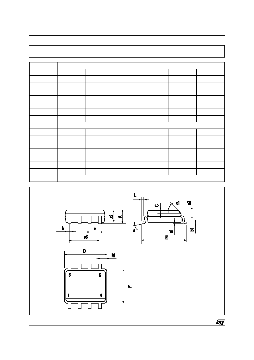
DIM.
mm
inch
MIN.
TYP.
MAX.
MIN.
TYP.
MAX.
A
1.75
0.068
a1
0.1
0.25
0.003
0.009
a2
1.65
0.064
a3
0.65
0.85
0.025
0.033
b
0.35
0.48
0.013
0.018
b1
0.19
0.25
0.007
0.010
C
0.25
0.5
0.010
0.019
c1
45 (typ.)
D
4.8
5.0
0.188
0.196
E
5.8
6.2
0.228
0.244
e
1.27
0.050
e3
3.81
0.150
F
3.8
4.0
0.14
0.157
L
0.4
1.27
0.015
0.050
M
0.6
0.023
S
8 (max.)
0016023
SO-8 MECHANICAL DATA
STS3DPFS30L
4/5

Information furnished is believed to be accurate and reliable. However, STMicroelectronics assumes no responsibility for the consequences
of use of such information nor for any infringement of patents or other rights of third parties which may result from its use. No license is
granted by implication or otherwise under any patent or patent rights of STMicroelectronics. Specification mentioned in this publication are
subject to change without notice. This publication supersedes and replaces all information previously supplied. STMicroelectronics products
are not authorized for use as critical components in life support devices or systems without express written approval of STMicroelectronics.
The ST logo is a trademark of STMicroelectronics
© 2000 STMicroelectronics ≠ Printed in Italy ≠ All Rights Reserved
STMicroelectronics GROUP OF COMPANIES
Australia - Brazil - China - Finland - France - Germany - Hong Kong - India - Italy - Japan - Malaysia - Malta - Morocco -
Singapore - Spain - Sweden - Switzerland - United Kingdom - U.S.A.
http://www.st.com
STS3DPFS30L
5/5