1/8
April 2002
STS4DPFS20L
P-CHANNEL 20V - 0.07
- 4A SO-8
STripFETTM MOSFET PLUS SCHOTTKY RECTIFIER
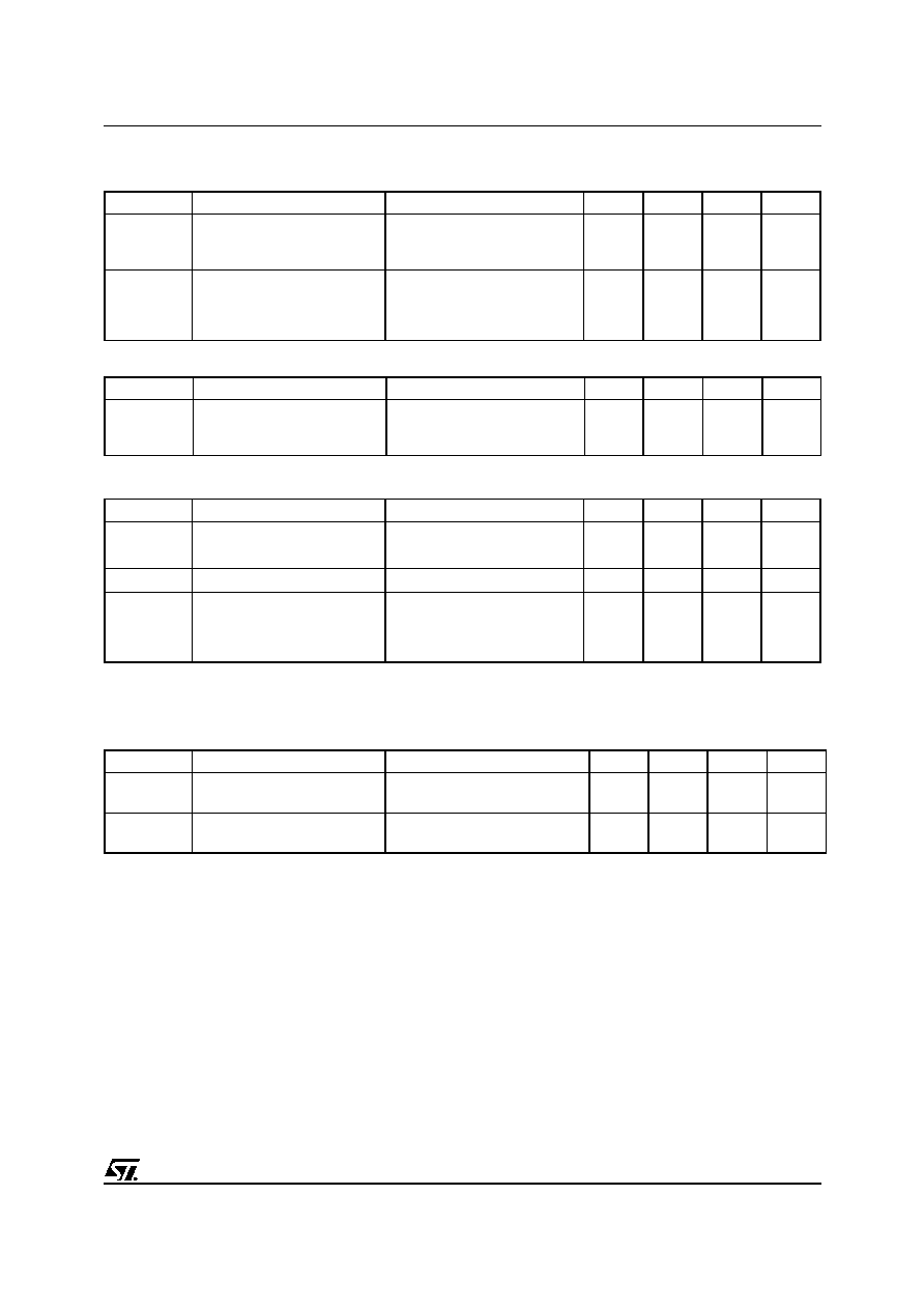
DESCRIPTION
This product associates the latest low voltage
STripFETTM in p-channel version to a low drop
Schottky diode. Such configuration is extremely ver-
satile in implementing, a large variety of DC-DC
converters for printers, portable equipment, and cel-
lular phones.
MOSFET ABSOLUTE MAXIMUM RATINGS
SCHOTTKY ABSOLUTE MAXIMUM RATINGS
(∑)Pulse width limited by safe operating area
MAIN PRODUCT CHARACTERISTICS
MOSFET
V
DSS
R
DS(on)
I
D
20 V
< 0.08
4 A
SCHOTTKY
I
F(AV)
V
RRM
V
F(MAX)
3 A
30 V
0.51 V
Symbol
Parameter
Value
Unit
V
DS
Drain-source Voltage (V
GS
= 0)
20
V
V
DGR
Drain-gate Voltage (R
GS
= 20 k
)
20
V
V
GS
Gate- source Voltage
± 16
V
I
D
Drain Current (continuos) at T
C
= 25∞C
4
A
I
D
Drain Current (continuos) at T
C
= 100∞C
3.4
A
I
DM
(
q
)
Drain Current (pulsed)
16
A
P
TOT
Total Dissipation at T
C
= 25∞C
2
W
Symbol
Parameter
Value
Unit
V
RRM
Repetitive Peak Reverse Voltage
30
V
I
F(RMS)
RMS Forward Current
20
A
I
F(AV)
Average Forward Current
TL = 125∞C
= 0.5
3
A
I
FSM
Surge Non Repetitive Forward Current
tp = 10 ms
Sinusoidal
75
A
I
RRM
Repetitive Peak Reverse Current
tp = 2
µ
s
F = 1 kHz
1
A
I
RSM
Non Repetitive Peak Reverse Current
tp = 100
µ
s
1
A
dv/dt
Critical Rate Of Rise Of Reverse Voltage
10000
V/
µ
s
Note: For the P-CHANNEL MOSFET actual polarity of Voltages
and current has to be reversed
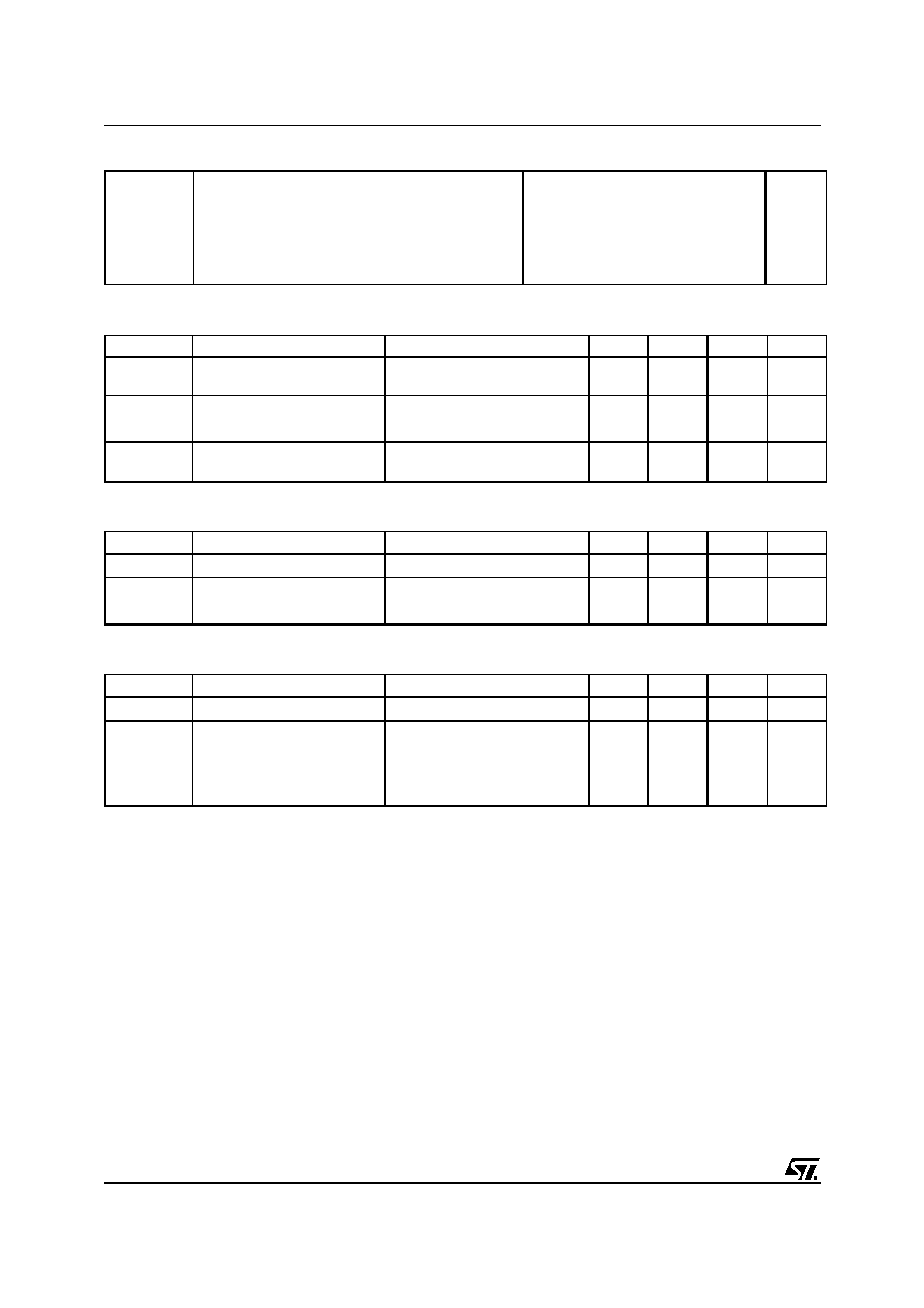
SO-8
INTERNAL SCHEMATIC DIAGRAM
STS4DPFS20L
2/8
THERMAL DATA
MOSFET ELECTRICAL CHARACTERISTICS (TCASE = 25 ∞C UNLESS OTHERWISE SPECIFIED)
OFF
ON (1)
DYNAMIC
Rthj-amb
(*)Thermal Resistance Junction-ambient MOSFET
62.5
∞C/W
Rthj-amb
(*)Thermal Resistance Junction-ambient SCHOTTKY
100
∞C/W
T
stg
Storage Temperature Range
-55 to 150
∞C
T
l
Junction Temperature
150
∞C
(*) Mounted on FR-4 board (Steady State)
Symbol
Parameter
Test Conditions
Min.
Typ.
Max.
Unit
V
(BR)DSS
Drain-source
Breakdown Voltage
I
D
= 250 µA, V
GS
= 0
20
V
I
DSS
Zero Gate Voltage
Drain Current (V
GS
= 0)
V
DS
= Max Rating
1
µA
V
DS
= Max Rating, T
C
= 125 ∞C
10
µA
I
GSS
Gate-body Leakage
Current (V
DS
= 0)
V
GS
= ± 16 V
±100
nA
Symbol
Parameter
Test Conditions
Min.
Typ.
Max.
Unit
V
GS(th)
Gate Threshold Voltage
V
DS
= V
GS
, I
D
= 250µA
1
V
R
DS(on)
Static Drain-source On
Resistance
V
GS
= 10V, I
D
= 2 A
0.07
0.08
V
GS
= 4.5V, I
D
= 2 A
0.085
0.10
Symbol
Parameter
Test Conditions
Min.
Typ.
Max.
Unit
g
fs
(1)
Forward Transconductance
V
DS
= 15V
,
I
D
= 2 A
10
S
C
iss
Input Capacitance
V
DS
= 25V, f = 1 MHz, V
GS
= 0
1350
pF
C
oss
Output Capacitance
490
pF
C
rss
Reverse Transfer
Capacitance
130
pF
3/8
STS4DPFS20L
ELECTRICAL CHARACTERISTICS (CONTINUED)
SWITCHING ON
SWITCHING OFF
SOURCE DRAIN DIODE
Note: 1. Pulsed: Pulse duration = 300 µs, duty cycle 1.5 %.
2. Pulse width limited by safe operating area.
SCHOTTCKY STATIC ELETTRICAL CHARACTERISTICS
Symbol
Parameter
Test Conditions
Min.
Typ.
Max.
Unit
t
d(on)
Turn-on Delay Time
V
DD
= 15V, I
D
= 2A R
G
= 4.7
V
GS
= 10V
(see test circuit, Figure 3)
25
ns
t
r
Rise Time
35
ns
Q
g
Total Gate Charge
V
DD
= 24V, I
D
= 4A,
V
GS
= 4.5 V
12.5
16
nC
Q
gs
Gate-Source Charge
5
nC
Q
gd
Gate-Drain Charge
3
nC
Symbol
Parameter
Test Conditions
Min.
Typ.
Max.
Unit
t
d(off)
t
f
Turn-off Delay Time
Fall Time
V
DD
= 15 V, I
D
= 2A,
R
G
= 4.7
,
V
GS
= 4.5 V
(see test circuit, Figure 3)
125
30
ns
ns
Symbol
Parameter
Test Conditions
Min.
Typ.
Max.
Unit
I
SD
Source-drain Current
4
A
I
SDM
(2)
Source-drain Current (pulsed)
16
A
V
SD
(1)
Forward On Voltage
I
SD
= 4 A, V
GS
= 0
1.2
V
t
rr
Reverse Recovery Time
I
SD
= 4 A, di/dt = 100A/µs,
V
DD
= 15 V, T
j
= 150∞C
(see test circuit, Figure 5)
45
ns
Q
rr
Reverse Recovery Charge
36
nC
I
RRM
Reverse Recovery Current
1.6
A
Symbol
Parameter
Test Conditions
Min.
Typ.
Max.
Unit
I
R
(*)
Reversed Leakage Current
T
J
= 25 ∞C , V
R
= 30 V
T
J
= 125 ∞C , V
R
= 30 V
0.03
0.2
100
mA
mA
V
F
(*)
Forward Voltage Drop
T
J
= 25 ∞C , I
F
= 3 A
T
J
= 125 ∞C , I
F
= 3 A
0.46
0.51
0.46
V
V
STS4DPFS20L
4/8
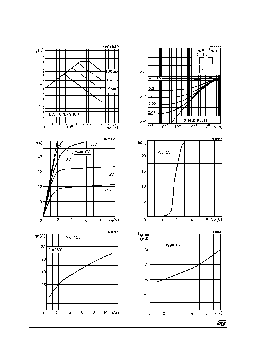
Transconductance
Static Drain-source On Resistance
Output Characteristics
Safe Operating Area
Thermal Impedance
Transfer Characteristics
5/8
STS4DPFS20L
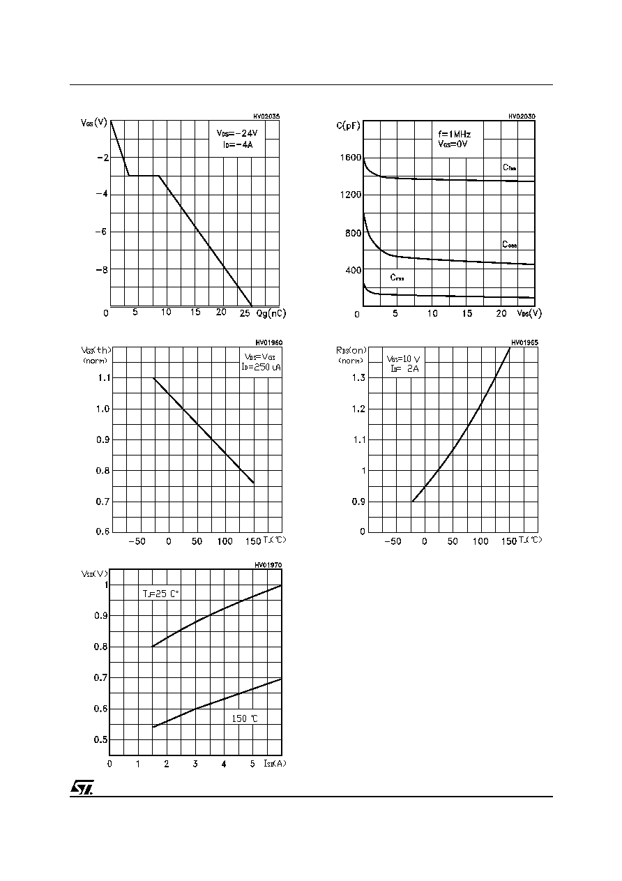
Normalized On Resistance vs Temperature
Source-drain Diode Forward Characteristics
Normalized Gate Threshold Voltage vs Temp.
Capacitance Variations
Gate Charge vs Gate-source Voltage