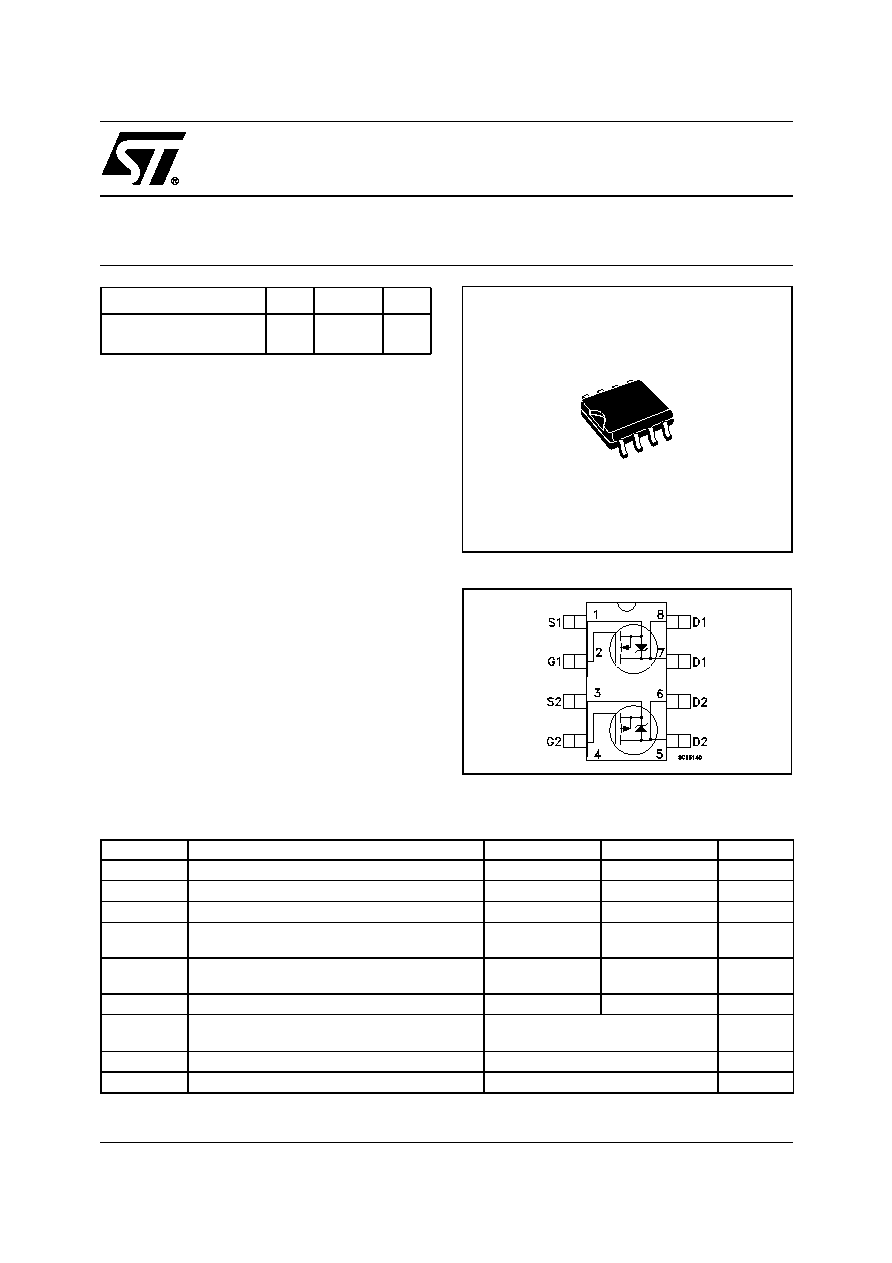
N-CHANNEL 30V - 0.018
- 7A SO-8
P-CHANNEL 30V - 0.070
- 4A SO-8
STripFETTM POWER MOSFET
1/10
June 2001
.
STS7C4F30L
s
TYPICAL R
DS
(on) (N-Channel) = 0.018
s
TYPICAL R
DS
(on) (P-Channel) = 0.070
s
STANDARD OUTLINE FOR EASY
AUTOMATED SURFACE MOUNT ASSEMBLY
s
LOW THRESHOLD DRIVE
DESCRIPTION
This Power MOSFET is the latest development of
STMicroelectronis unique "Single Feature SizeTM"
strip-based process. The resulting transistor
shows extremely high packing density for low on-
resistance, rugged avalanche characteristics and
less critical alignment steps therefore a remark-
able manufacturing reproducibility.
APPLICATIONS
s
DC/DC CONVERTERS
s
BATTERY MANAGEMENT IN NOMADIC
EQUIPMENT
s
POWER MANAGEMENT IN CELLULAR
PHONES
TYPE
V
DSS
R
DS(on)
I
D
STS7C4F30L(N-Channel)
STS7C4F30L(P-Channel)
30 V
30 V
<0.022
<0.080
7 A
4 A
SO-8
ABSOLUTE MAXIMUM RATINGS
(
�)
Pulse width limited by safe operating area.
Note: P-CHANNEL MOSFET actual polarity of voltages and current
has to be reversed
Symbol
Parameter
N-CHANNEL
P-CHANNEL
Unit
V
DS
Drain-source Voltage (V
GS
= 0)
30
30
V
V
DGR
Drain-gate Voltage (R
GS
= 20 k
)
30
30
V
V
GS
Gate- source Voltage
� 20
� 20
V
I
D
Drain Current (continuos) at T
C
= 25�C
Single Operating
7
4
A
I
D
Drain Current (continuos) at T
C
= 100�C
Single Operating
4.4
2.5
A
I
DM
(
�)
Drain Current (pulsed)
28
16
A
P
tot
Total Dissipation at T
C
= 25�C Dual Operating
Total Dissipation at T
C
= 25�C Single Operating
1.6
2
W
W
T
stg
Storage Temperature
-60 to 150
�C
T
j
Max. Operating Junction Temperature
150
�C
INTERNAL SCHEMATIC DIAGRAM
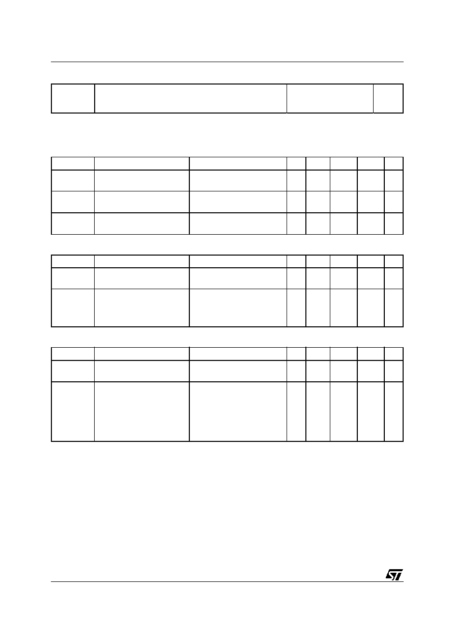
STS7C4F30L
2/10
THERMAL DATA
(1)
when mounted on 0.5 in
2
pad of 2 oz. copper
ELECTRICAL CHARACTERISTICS (T
case
= 25 �C unless otherwise specified)
OFF
ON
DYNAMIC
Rthj-amb
(1)
T
l
Thermal Resistance Junction-ambient
Single Operation
Dual Operating
Maximum Lead Temperature For Soldering Purpose
62.5
78
300
�C/W
�C/W
�C
Symbol
Parameter
Test Conditions
Min.
Typ.
Max.
Unit
V
(BR)DSS
Drain-source
Breakdown Voltage
I
D
= 250 �A, V
GS
= 0
n-ch
p-ch
30
30
V
I
DSS
Zero Gate Voltage
Drain Current (V
GS
= 0)
V
DS
= Max Rating
V
DS
= Max Rating T
C
= 125�C
1
10
�A
�A
I
GSS
Gate-body Leakage
Current (V
DS
= 0)
V
GS
= � 20V
V
GS
= � 20V
n-ch
p-ch
�100
�100
nA
nA
Symbol
Parameter
Test Conditions
Min.
Typ.
Max.
Unit
V
GS(th)
Gate Threshold Voltage
V
DS
= V
GS
I
D
= 250 �A
n-ch
p-ch
1
1
1.6
1.6
2.5
2.5
V
V
R
DS(on)
Static Drain-source On
Resistance
V
GS
= 10 V
I
D
= 3.5 A
V
GS
= 10 V
I
D
= 2 A
V
GS
= 4.5 V
I
D
= 3.5 A
V
GS
= 4.5 V
I
D
= 2 A
n-ch
p-ch
n-ch
p-ch
0.018
0.070
0.021
0.085
0.022
0.080
0.026
0.10
Symbol
Parameter
Test Conditions
Min.
Typ.
Max.
Unit
g
fs (*)
Forward Transconductance
V
DS
= 15 V
I
D
= 3.5 A
V
DS
= 15 V
I
D
= 2 A
n-ch
p-ch
10
10
S
S
C
iss
C
oss
C
rss
Input Capacitance
Output Capacitance
Reverse Transfer
Capacitance
V
DS
= 25V, f = 1 MHz, V
GS
= 0
n-ch
p-ch
n-ch
p-ch
n-ch
p-ch
1050
1350
250
490
85
130
pF
pF
pF
pF
pF
pF
3/10
STS7C4F30L
SWITCHING ON
SWITCHING OFF
SOURCE DRAIN DIODE
(
)
Pulsed: Pulse duration = 300 �s, duty cycle 1.5 %.
(
�)
Pulse width limited by safe operating area.
Symbol
Parameter
Test Conditions
Min.
Typ.
Max.
Unit
t
d(on)
t
r
Turn-on Delay Time
Rise Time
N-CHANNEL
V
DD
= 15 V
I
D
= 3.5 A
R
G
= 4.7
V
GS
= 4.5 V
P-CHANNEL
V
DD
= 15 V
I
D
= 2 A
R
G
= 4.7
V
GS
= 4.5 V
(Resistive Load, Figure 1)
n-ch
p-ch
n-ch
p-ch
22
25
60
35
ns
ns
ns
ns
Qg
Q
gs
Q
gd
Total Gate Charge
Gate-Source Charge
Gate-Drain Charge
N-CHANNEL
V
DD
= 24V I
D
= 7A V
GS
= 5V
P-CHANNEL
V
DD
= 24V I
D
= 4A V
GS
= 5V
(see test circuit, Figure 2)
n-ch
p-ch
n-ch
p-ch
n-ch
p-ch
17.5
12.5
4
5
7
3
23
16
nC
nC
nC
nC
nC
nC
Symbol
Parameter
Test Conditions
Min.
Typ.
Max.
Unit
t
d(off)
t
f
Turn-off Delay Time
Fall Time
N-CHANNEL
V
DD
= 15 V
I
D
= 3.5 A
R
G
= 4.7
V
GS
= 4.5 V
P-CHANNEL
V
DD
= 15 V
I
D
= 2 A
R
G
= 4.7
V
GS
= 4.5 V
(Resistive Load, Figure 1)
n-ch
p-ch
n-ch
p-ch
42
125
10
35
ns
ns
ns
ns
Symbol
Parameter
Test Conditions
Min.
Typ.
Max.
Unit
I
SD
I
SDM
(
�)
Source-drain Current
Source-drain Current (pulsed)
n-ch
p-ch
n-ch
p-ch
7
4
28
16
A
A
A
A
V
SD
(
)
Forward On Voltage
I
SD
= 7 A
V
GS
= 0
I
SD
= 4 A
V
GS
= 0
n-ch
p-ch
1.2
1.2
V
V
t
rr
Q
rr
I
RRM
Reverse Recovery Time
Reverse Recovery Charge
Reverse Recovery Current
N-CHANNEL
I
SD
= 7 A
di/dt = 100A/
�
s
V
DD
= 15
V
T
j
=150
o
C
P-CHANNEL
I
SD
= 4 A
di/dt = 100A/
�
s
V
DD
= 15
V
T
j
=150
o
C
(see test circuit, Figure 3)
n-ch
p-ch
n-ch
p-ch
n-ch
p-ch
50
45
40
36
1.6
1.6
ns
ns
nC
nC
A
A
ELECTRICAL CHARACTERISTICS (continued)
STS7C4F30L
4/10
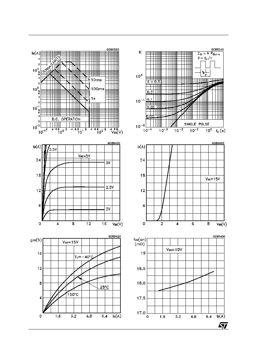
Safe Operating Area
n-ch
Thermal Impedance
n-ch
Output Characteristics
n-ch
Transfer Characteristics
n-ch
Transconductance
n-ch
Static Drain-source On Resistance
n-ch
5/10
STS7C4F30L
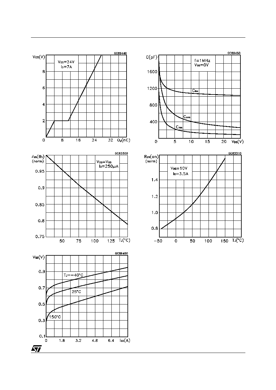
Gate Charge vs Gate-source Voltage
n-ch
Capacitance Variations
n-ch
Normalized Gate Threshold Voltage vs Temperature
n-ch
Normalized on Resistance vs Temperature
n-ch
Source-drain Diode Forward Characteristics
n-ch