
1/6
TARGET DATA
June 2003
STSJ20NM20N
N-CHANNEL 200V - 0.11
- 20A PowerSO-8TM
ULTRA LOW GATE CHARGE MDmeshTMII MOSFET
s
WORLDWIDE LOWEST GATE CHARGE
s
TYPICAL R
DS
(on) = 0.11
s
HIGH dv/dt AND AVALANCHE CAPABILITIES
s
LOW INPUT CAPACITANCE
s
LOW GATE RESISTANCE
s
TIGHT PROCESS CONTROL AND HIGH
MANUFACTORING YIELDS
DESCRIPTION
This 200V MOSFET with a new advanced layout
brings all unique advantages of MDmesh technolo-
gy to lower voltages. The device exhibits worldwide
lowest gate charge for any given on-resistance.Its
use is therefore ideal as primary switch in isolated
DC-DC converters for Telecom and Computer appli-
cations.Used in combination with secondary-side
low-voltage STripFET
TM
products, it contributes to
reducing losses and boosting efficiency.The ex-
posed slug reduced the Rthj-c improving the current
capability
APPLICATIONS
The MDmeshTM family is very suitable for increasing
power density allowing system miniaturization and
higher efficiencies.
ORDERING INFORMATION
TYPE
V
DSS
R
DS(on)
I
D
STSJ20NM20N
200 V
< 0.13
20 A
SALES TYPE
MARKING
PACKAGE
PACKAGING
STSJ20NM20N
SJ20NM20N
PowerSO-8
TAPE & REEL
PowerSO-8
INTERNAL SCHEMATIC DIAGRAM
DRAIN CONTACT ALSO ON THE BACKSIDE

STSJ20NM20N
2/6
ABSOLUTE MAXIMUM RATINGS
THERMAL DATA
AVALANCHE CHARACTERISTICS
ELECTRICAL CHARACTERISTICS (T
CASE
= 25 ∞C UNLESS OTHERWISE SPECIFIED)
ON/OFF
Symbol
Parameter
Value
Unit
V
DS
Drain-source Voltage (V
GS
= 0)
200
V
V
DGR
Drain-gate Voltage (R
GS
= 20 k
)
200
V
V
GS
Gate-source Voltage
± 30
V
I
D
Drain Current (continuous) at T
C
= 25∞C
Drain Current (continuous) at T
C
= 100∞C
20
12.5
A
A
I
DM
(2)
Drain Current (pulsed)
80
A
P
TOT
P
TOT
Total Dissipation at T
C
= 25∞C
Total Dissipation at T
C
= 25∞C (1)
70
3
W
W
dv/dt (3)
Peak Diode Recovery voltage slope
10
V/ns
Rthj-c
Thermal Resistance Junction-case Max
1.8
∞C/W
Rthj-amb
Thermal Resistance Junction-ambient Max (1)
42
∞C/W
T
j
Max. Operating Junction Temperature
150
∞C
T
stg
Storage Temperature
≠ 55 to 150
∞C
Symbol
Parameter
Max Value
Unit
I
AR
Avalanche Current, Repetitive or Not-Repetitive
(pulse width limited by T
j
max)
TBD
A
E
AS
Single Pulse Avalanche Energy
(starting T
j
= 25 ∞C, I
D
= I
AR
, V
DD
= 35 V)
TBD
mJ
Symbol
Parameter
Test Conditions
Min.
Typ.
Max.
Unit
V
(BR)DSS
Drain-source
Breakdown Voltage
I
D
= 1 mA, V
GS
= 0
200
V
I
DSS
Zero Gate Voltage
Drain Current (V
GS
= 0)
V
DS
= Max Rating
V
DS
= Max Rating, T
C
= 125 ∞C
1
10
µA
µA
I
GSS
Gate-body Leakage
Current (V
DS
= 0)
V
GS
= ± 30V
100
nA
V
GS(th)
Gate Threshold Voltage
V
DS
= V
GS
, I
D
= 250 µA
3.5
4.2
5
V
R
DS(on)
Static Drain-source On
Resistance
V
GS
= 10 V, I
D
= 2 A
0.11
0.13

3/6
STSJ20NM20N
ELECTRICAL CHARACTERISTICS (CONTINUED)
DYNAMIC
(*) C
oss eq.
is defined as a constant equivalent capacitance giving the same charging time as C
oss
when V
DS
increases from 0 to 80% V
DSS
SWITCHING ON
SWITCHING OFF
SOURCE DRAIN DIODE
Note: 1. When mounted on FR4 Board with 1inch≤ pad, 2oz of Cu, t
10 sec.
2. Pulse width limited by safe operating area
3. I
SD
20A, di/dt
400A/µs, V
DD
V
(BR)DSS
, T
J
T
JMAX
4. Pulsed: Pulse duration = 400 µs, duty cycle 1.5 %
Symbol
Parameter
Test Conditions
Min.
Typ.
Max.
Unit
g
fs
(4)
Forward Transconductance
V
DS
= 15 V
,
I
D
= 2 A
1.4
S
C
iss
C
oss
C
rss
Input Capacitance
Output Capacitance
Reverse Transfer
Capacitance
V
DS
= 25 V, f = 1 MHz, V
GS
= 0
670
180
12
pF
pF
pF
C
oss eq.
(*)
Equivalent Output
Capacitance
V
GS
= 0V, V
DS
= 0V to 400V
TBD
pF
R
G
Gate Input Resistance
f=1 MHz Gate DC Bias = 0
Test Signal Level = 20mV
Open Drain
TBD
Symbol
Parameter
Test Conditions
Min.
Typ.
Max.
Unit
t
d(on)
t
r
Turn-on Delay Time
Rise Time
V
DD
= 100 V, I
D
= 2 A
R
G
= 4.7
V
GS
= 10 V
(see test circuit, Figure 3)
TBD
TBD
ns
ns
Q
g
Q
gs
Q
gd
Total Gate Charge
Gate-Source Charge
Gate-Drain Charge
V
DD
= 160 V, I
D
= 4 A,
V
GS
= 10 V
19
3.5
11
nC
nC
nC
Symbol
Parameter
Test Conditions
Min.
Typ.
Max.
Unit
t
r(Voff)
t
f
t
c
Off-Voltage Rise Time
Fall Time
Cross-Over Time
V
DD
= 100 V, I
D
= 2 A,
R
G
= 4.7
,
V
GS
= 10 V
(see test circuit, Figure 3)
TBD
TBD
TBD
ns
ns
ns
Symbol
Parameter
Test Conditions
Min.
Typ.
Max.
Unit
I
SD
I
SDM
(2)
Source-drain Current
Source-drain Current (pulsed)
20
80
A
A
V
SD
(4)
Forward On Voltage
I
SD
= 2 A, V
GS
= 0
1.3
V
t
rr
Q
rr
I
RRM
Reverse Recovery Time
Reverse Recovery Charge
Reverse Recovery Current
I
SD
= 2 A, di/dt = 100 A/µs,
V
DD
= 100 V, T
j
= 25∞C
(see test circuit, Figure 5)
89
300
6.5
ns
nC
A
t
rr
Q
rr
I
RRM
Reverse Recovery Time
Reverse Recovery Charge
Reverse Recovery Current
I
SD
= 2 A, di/dt = 100 A/µs,
V
DD
= 100 V, T
j
= 150∞C
(see test circuit, Figure 5)
TBD
TBD
TBD
ns
nC
A
STSJ20NM20N
4/6
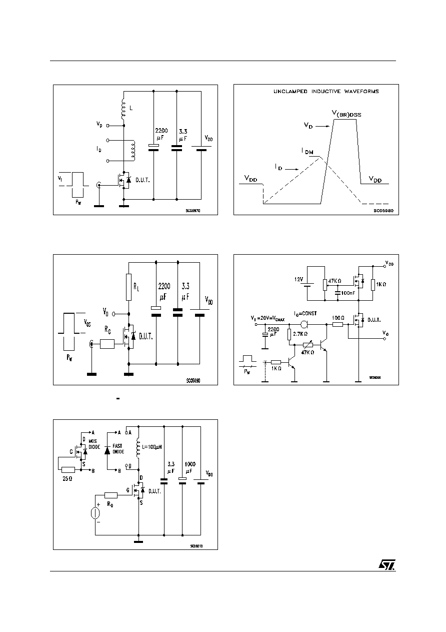
Fig. 5: Test Circuit For Inductive Load Switching
And Diode Recovery Times
Fig. 4: Gate Charge test Circuit
Fig. 2: Unclamped Inductive Waveform
Fig. 1: Unclamped Inductive Load Test Circuit
Fig. 3: Switching Times Test Circuit For
Resistive Load
5/6
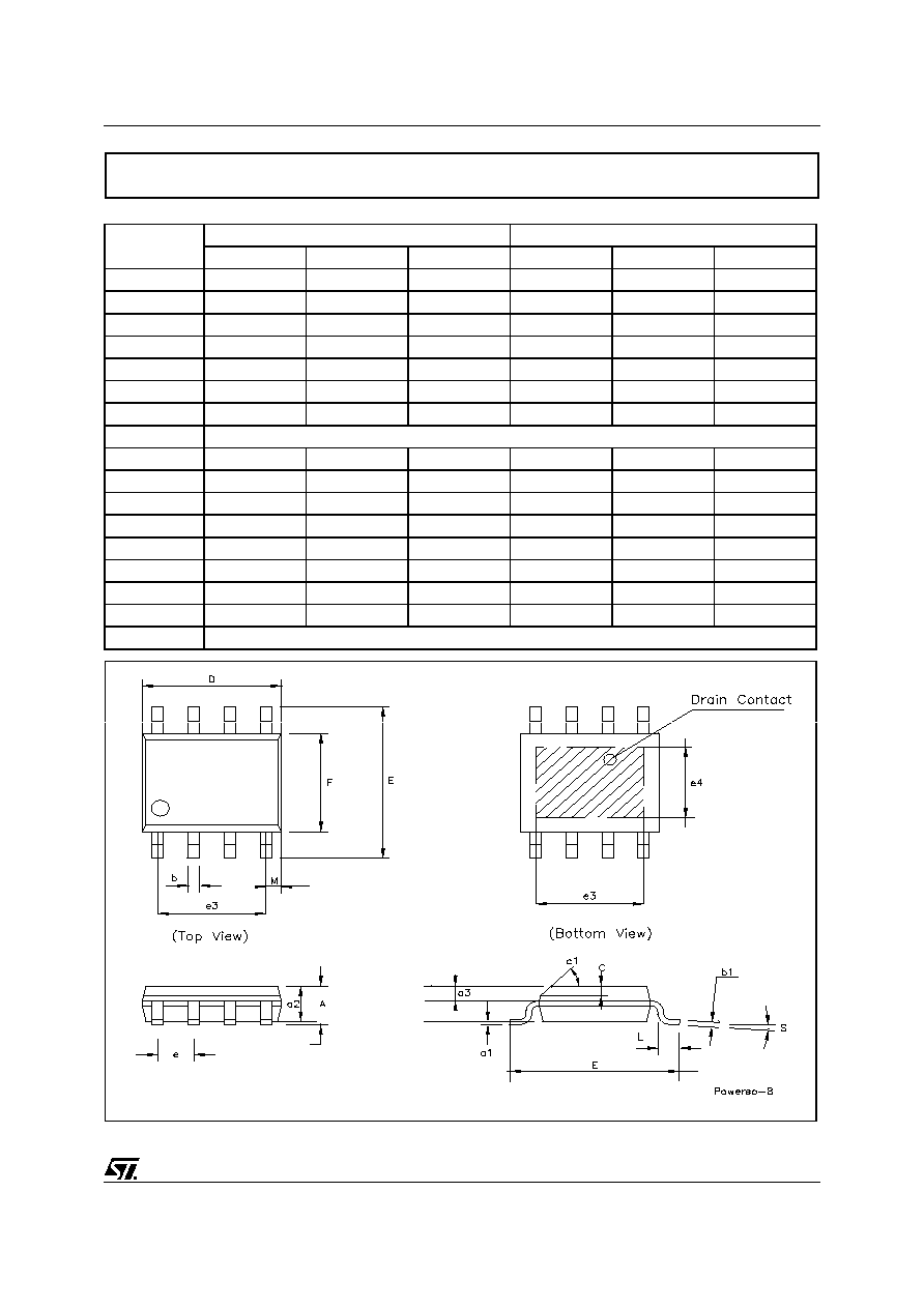
STSJ20NM20N
DIM.
mm.
inch
MIN.
TYP
MAX.
MIN.
TYP.
MAX.
A
1.75
0.068
a1
0.1
0.25
0.003
0.009
a2
1.65
0.064
a3
0.65
0.85
0.025
0.033
b
0.35
0.48
0.013
0.018
b1
0.19
0.25
0.007
0.010
C
0.25
0.5
0.010
0.019
c1
45∞ (typ.)
D
4.8
5.0
0.188
0.196
E
5.8
6.2
0.228
0.244
e
1.27
0.050
e3
3.81
0.150
e4
2.79
0.110
F
3.8
4.0
0.14
0.157
L
0.4
1.27
0.015
0.050
M
0.6
0.023
S
8∞ (max.)
PowerSO-8TM MECHANICAL DATA