April 2006
Rev 1
1/12
12
STSJ60NH3LL
N-channel 30V - 0.004
- 15A - PowerSO-8TM
STripFETTM Power MOSFET for DC-DC conversion
General features
Optimal R
DS(on)
x Qg trade-off @ 4.5 V
Conduction losses reduced
Improved junction-case thermal resistance
Low threshold device
Description
This device utilizes the latest advanced design
rules of ST's proprietary STripFETTM technology.
This process coupled to unique metallization
techniques realizes the most advanced low
voltage Power MOSFET in SO-8 ever produced.
The exposed slug reduces the Rthj-c improving
the current capability.
Applications
Switching application
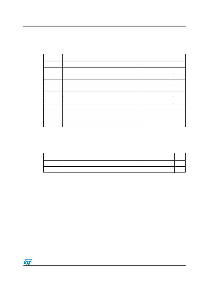
Internal schematic diagram
Type
V
DSS
R
DS(on)
I
D
STSJ60NH3LL
30V
<0.0057
15A
(2)
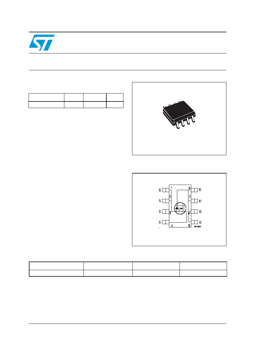
PowerSO-8TM
DRAIN CONTACT ALSO ON THE BACKSIDE
www.st.com
Order codes
Part number
Marking
Package
Packaging
STSJ60NH3LL
60H3LL-
PowerSO-8TM Tape
&
reel

Contents
STSJ60NH3LL
2/12
Contents
1
Electrical ratings . . . . . . . . . . . . . . . . . . . . . . . . . . . . . . . . . . . . . . . . . . . . 3
2
Electrical characteristics . . . . . . . . . . . . . . . . . . . . . . . . . . . . . . . . . . . . . 4
2.1
Electrical characteristics (curves) . . . . . . . . . . . . . . . . . . . . . . . . . . . . 6
3
Test circuit . . . . . . . . . . . . . . . . . . . . . . . . . . . . . . . . . . . . . . . . . . . . . . . . 8
4
Package mechanical data . . . . . . . . . . . . . . . . . . . . . . . . . . . . . . . . . . . . . 9
5
Revision history . . . . . . . . . . . . . . . . . . . . . . . . . . . . . . . . . . . . . . . . . . . 11
STSJ60NH3LL
Electrical ratings
3/12
1 Electrical
ratings
Table 1.
Absolute maximum ratings
Symbol
Parameter
Value
Unit
V
DS
Drain-source voltage (V
GS
= 0)
30
V
V
GS
Gate- source voltage
± 16
V
I
D
(1)
1.
This value is rated according to Rthj-c
Drain current (continuous) at T
C
= 25∞C
60
A
I
D
Drain current (continuous) at T
C
= 100∞C
37.5
A
I
D
(2)
2.
This value is rated according to Rthj-pcb
Drain current (continuous) at T
C
= 25∞C
15
A
I
D
Drain current (continuous) at T
C
= 100∞C
9.4
A
I
DM
(3)
3.
Pulse width limited by safe operating area
Drain current (pulsed)
60
A
P
tot
(1)
Total dissipation at T
C
= 25∞C
50
W
P
tot
(2)
Total dissipation at T
C
= 25∞C
3
W
T
stg
Storage temperature
-55 to 150
∞C
Tj
Operating junction temperature
Table 2.
Thermal resistance
Symbol
Parameter
Value
Unit
Rthj-case
Thermal resistance junction-case (drain) Max
2.5
∞C/W
Rthj-amb
Thermal resistance junction-ambient Max
42
∞C/W
Electrical characteristics
STSJ60NH3LL
4/12
2 Electrical
characteristics
(T
CASE
=25∞C unless otherwise specified)
Table 3.
On/off states
Symbol
Parameter
Test condictions
Min.
Typ.
Max.
Unit
V
(BR)DSS
Drain-source
breakdown voltage
I
D
= 250 µA, V
GS
= 0
30
V
I
DSS
Zero gate voltage
drain current (V
GS
= 0)
V
DS
= Max rating
V
DS
= Max rating @125∞C
1
10
µA
µA
I
GSS
Gate-body leakage
current (V
DS
= 0)
V
GS
= ± 16V
±100
nA
V
GS(th)
Gate threshold voltage
V
DS
= V
GS
, I
D
= 250µA
1
V
R
DS(on)
Static drain-source on
resistance
V
GS
= 10V, I
D
= 7.5A
V
GS
= 4.5V, I
D
= 7.5A
0.004
0.005
0.0057
0.0075
Table 4.
Dynamic
Symbol
Parameter
Test condictions
Min.
Typ.
Max.
Unit
C
iss
C
oss
C
rss
Input capacitance
Output capacitance
Reverse transfer
capacitance
V
DS
=25V, f=1MHz, V
GS
= 0
1810
565
41
pF
pF
pF
Q
g
Q
gs
Q
gd
Total gate charge
Gate-source charge
Gate-drain charge
V
DD
=15V, I
D
=15A
V
GS
=4.5V
(see Figure 13)
18
4.8
5.3
24
nC
nC
nC
R
G
Gate input resistance
f=1 MHz Gate DC Bias = 0
Test signal level = 20mV
open drain
0.5
1.5
3
STSJ60NH3LL
Electrical characteristics
5/12
Table 5.
Switching times
Symbol
Parameter
Test condictions
Min.
Typ.
Max. Unit
t
d(on)
t
r
Turn-on delay time
Rise Time
V
DD
= 15V, I
D
= 7.5A
R
G
= 4.7
, V
GS
= 10V
(see Figure 12)
8
65
ns
ns
t
d(off)
t
f
Turn-off delay time
Fall time
V
DD
= 15V, I
D
= 7.5A
R
G
= 4.7
,
V
GS
= 10V
(see Figure 12)
38
20
ns
ns
Table 6.
Source drain diode
Symbol
Parameter
Test condictions
Min
Typ.
Max
Unit
I
SD
I
SDM
Source-drain current
Source-drain current (pulsed)
15
60
A
A
V
SD
(1)
1.
Pulsed: pulse duration=300µs, duty cycle 1.5%
Forward On Voltage
I
SD
= 15A, V
GS
= 0
1.3
V
t
rr
Q
rr
I
RRM
Reverse recovery time
Reverse recovery charge
Reverse recovery current
I
SD
= 15A, di/dt = 100A/µs
V
DD
= 15V, T
j
= 25∞C
(see Figure 17)
22
32
1.9
ns
nC
A