 | ÐлекÑÑоннÑй компоненÑ: STSR2CD | СкаÑаÑÑ:  PDF PDF  ZIP ZIP |
Äîêóìåíòàöèÿ è îïèñàíèÿ www.docs.chipfind.ru
1/12
June 2003
s
SUPPLY VOLTAGE RANGE: 4.5V TO 5.5V
s
TYPICAL PEAK OUTPUT CURRENT:
SOURCE -2A, SINK 3.5A
s
OPERATING FREQUENCY: 20 TO 750 KHZ
s
SMART TURN-OFF ANTICIPATION TIMING
s
OPERATION INDEPENDENT FROM THE
FORWARD MAGNETIC RESET TECHNIQUE
s
POSSIBILITY TO OPERATE IN
DISCONTINUOUS MODE
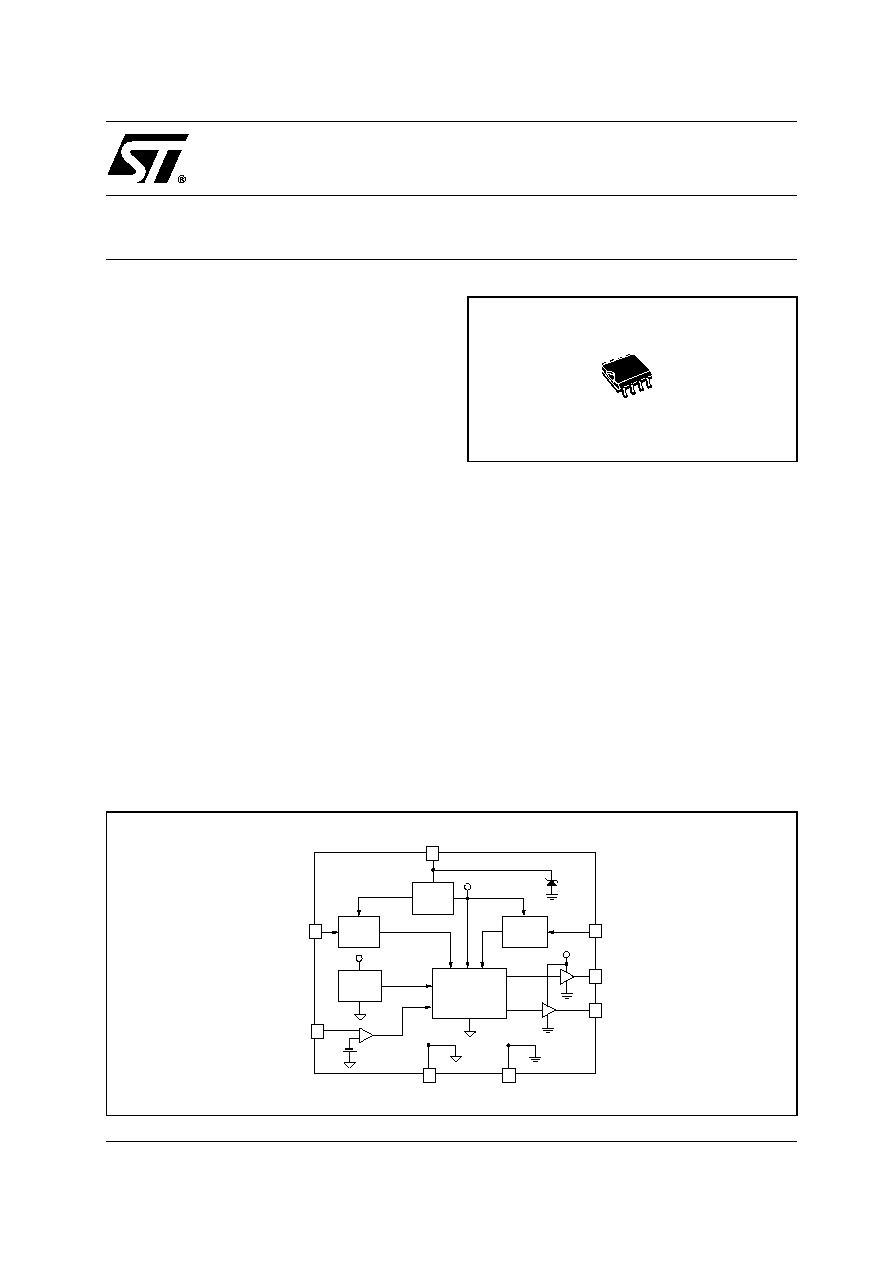
DESCRIPTION
STSR2
Smart
Driver
IC
provides
two
complementary high current outputs to drive
Power Mosfets. The IC is dedicated to properly
drive
secondary
Synchronous
Rectifiers
in
medium power, low output voltage, high efficiency
Forward Converters. From a synchronizing clock
input, STSR2 generates two driving signals with
the
self-setting
of
dead
time
between
complementary pulses. The IC operation prevents
secondary
side
shoot-through
conditions
providing proper timing at the outputs turn-off
transition. This smart function operates through a
fast cycle-after-cycle control logic mechanism
based on an internal high frequency oscillator,
synchronized
by
the
clock
signal.
A
fixed
anticipation in turning-off the OUT
GATE1
with
respect to the clock signal transition is provided,
while the anticipation in turning off the OUT
GATE2
can be set through external components. The
adopted transitions revelation mechanism makes
circuit operation independent by the forward
magnetic reset technique used, avoiding most of
the common problems inherent in self-driven
synchronous rectifiers. A special Inhibit function
allows the shut-off of OUT
GATE2
. This feature
makes discontinuous conduction mode possible
and prevents the freewheeling mosfet from
sinking current from the output.
STSR2 automatically turns off the outputs when
duty-cycle is lower than 13%, while STSR2M
works even at very low duty-cycle values.
STSR2
FORWARD SYNCHRONOUS
RECTIFIERS SMART DRIVER
PEAK
DETECTOR
BIAS
UVLO
CK
Vcc
6
5.7V
8
4
2
OUTPUT
BUFFERS
7
OUTGate2
PWRGND
SGLGND
ANTICIPATION
SET
3
SETANT2
5
INHIBIT
25mV
-
+
DIGITAL
CONTROL
HIGH
FREQUENCY
OSCILLATOR
1
OUTGate1
+
+
+
SCHEMATIC DIAGRAM
SO-8
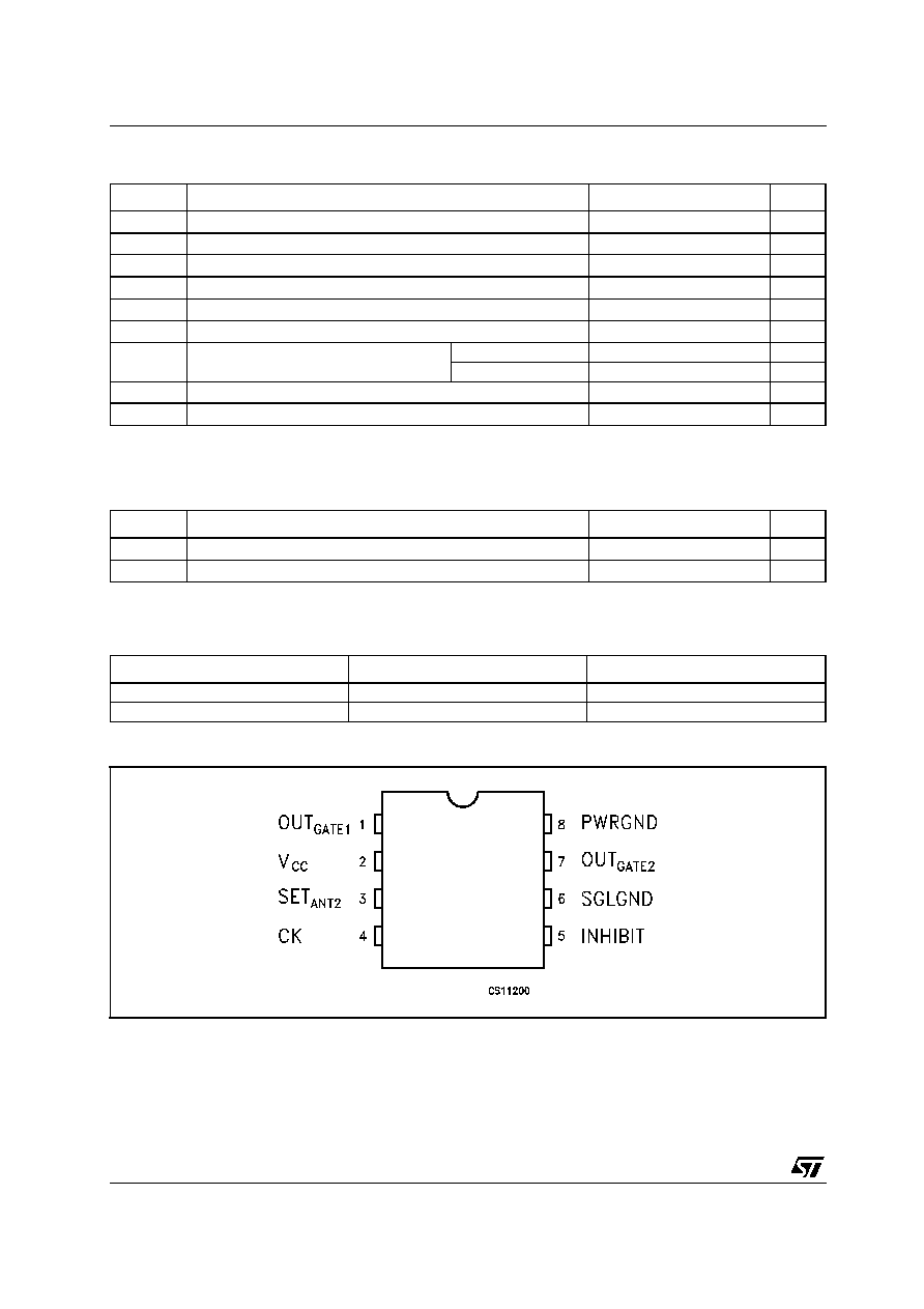
STSR2
2/12
ABSOLUTE MAXIMUM RATINGS
Absolute Maximum Ratings are those values beyond which damage to the device may occur. Functional operation under these condition is
not implied.
(*) A higher positive voltage level can be applied to the pin with a resistor which limits the current flowing into the pin to 10mA maximum
THERMAL DATA
(*) This value is referred to one layer pcb board with minimum copper connections for the leads. a minimum value of 120 °C/W can be
obtained improving thermal conductivity of the board
ORDERING CODES
CONNECTION DIAGRAM (top view)
Symbol
Parameter
Value
Unit
V
CC
DC Input Voltage
-0.3 to 6
V
V
OUTGATE
Max Gate Drive Output Voltage
-0.3 to V
CC
V
V
INHIBIT
Max INHIBIT Voltage (*)
-0.6 to V
CC
V
V
CK
Clock Input Voltage Range (*)
-0.3 to V
CC
V
I
LX
Switching Peak Current
2
A
P
TOT
Continuous Power Dissipation at T
A
=105°C without heatsink
270
mW
ESD
Human Body Model
Pins 1,2, 4, 5, 6, 7, 8
±
1
KV
Pin 3
±
0.9
KV
T
stg
Storage Temperature Range
-55 to +150
°C
T
op
Operating Junction Temperature Range
-40 to +125
°C
Symbol
Parameter
SO-8
Unit
R
thj-amb
Thermal Resistance Junction-case
40
°C/W
R
thj-amb
Thermal Resistance Junction-ambient (*)
160
°C/W
TYPE
SO-8
SO-8 (T&R)
STSR2
STSR2CD
STSR2CD-TR
STSR2M
STSR2MCD
STSR2MCD-TR
STSR2
3/12
PIN DESCRIPTION
Pin N°
Symbol
Name and Function
1
OUT
GATE1
Gate Drive signal for Rectifier MOSFET. Anticipation (t
ANT1
) in turning off
OUT
GATE1
is provided when the clock input goes to low level.
2
V
CC
The supply voltage range from 4.5V to 5.5V allows applications with logic gate
threshold mosfets. UVLO feature guarantees proper start-up while it avoids
undesirable driving during eventual dropping of the supply voltage.
3
SET
ANT2
The voltage on this pin sets the anticipation (t
ANT1
) in turning off the OUT
GATE2
. It
is possible to choose among three different anticipation times by discrete
partitioning of the supply voltage.
4
CK
This input provides synchronization for IC's operations, being the transitions
between the two output conditions based on a positive threshold, equal for the
two slopes. A smart internal control logic mechanism using a 15MHz internal
oscillator generates proper anticipation timing at the turn-off of each output. This
feature allows safe turn-off of Synchronous Rectifiers avoiding any eventual
shoot-through situation on secondary side at both transitions. Smart clock
revelation mechanism makes these operations independent by false triggering
pulses generated in light load conditions and by particular demagnetization
techniques.Absolute maximum voltage rating of the pin can be exceeded limiting
the current flowing into the pin to 10mA max.
5
INHIBIT
This input enables OUT
GATE2
to work when its voltage is lower than the negative
threshold voltage (V
INHIBIT
<V
H
). If V
INHIBIT
>V
H
the OUT
GATE2
will be high for a
minimum conduction time (t
ON(GATE2)
). In typical forward converter application, it
is possible to turn off the freewheeling MOSFET when the current through it tends
to reverse, allowing discontinuous conduction mode and providing protection to
the converter from eventual sinking current from the load.Absolute maximum
voltage rating of the pin can be exceeded limiting the current flowing into the pin
to 10mA max.
6
SGLGND
Reference for all the control logic signals. This pin is completely separated from
the PWRGND to prevent eventual disturbances to affect the control logic.
7
OUT
GATE2
Gate Drive signal for Freewheeling MOSFET. Anticipation [t
ANT2
] in turning off
OUT
GATE2
is provided when the clock input goes to high level.
8
PWRGND
Reference for power signals, this pin carries the full peak currents for the two
outputs.
STSR2
4/12
ELECTRICAL CHARACTERISTICS (V
CC
=5V, CK= 250kHz, V
INHIBIT
=-200mV, T
J
=-40 to 125°C, unless
otherwise specified.)
Note1: t
R
is measured between 10% and 90% of the final voltage; t
F
is measured between 90% and 10% on the initial voltage
Note2: Parameter guaranteed by design
Symbol
Parameter
Test Conditions
Min.
Typ.
Max.
Unit
SUPPLY INPUT AND UNDER VOLTAGE LOCK OUT
V
CCON
Start Threshold
3.8
4
V
V
CCOFF
Turn OFF Threshold After
Start
3.5
3.6
V
V
Z
Zener Voltage
CK=0V
I
Z
= 2mA
5.5
5.8
6
V
I
CC
Unloaded Supply Current
OUT
GATE1,2
= no load
22
30
mA
CK=0V
OUT
GATE1,2
= no load
3
5
GATE DRIVER OUTPUTS
V
OL
Output Low Voltage
I
OUTGATE1,2
=-200mA
0.10
0.16
V
V
OH
Output High Voltage
I
OUTGATE1,2
=200mA
4.70
4.85
V
I
OUT
Output Source Peak
Current
2
A
Output Sink Peak Current
3.5
R
OUT
Output Series Source
Resistance
I
OUTGATE1,2
=-200mA
0.75
1.5
Output Series Sink
Resistance
I
OUTGATE1,2
=200mA
0.5
0.8
t
R
OUT
GATE1,2
Rise Time
C
LOAD
=5nF (Note 1)
40
ns
t
F
OUT
GATE1,2
Fall Time
C
LOAD
=5nF (Note 1)
30
ns
t
P1
Clock Propagation Delay to
Turn ON of OUT
GATE1
No Load
130
ns
t
P2
Clock Propagation Delay to
Turn ON of OUT
GATE2
No Load
50
ns
TURN-OFF ANTICIPATION TIME
t
ANT1
OUT
GATE1
Turn-off
Anticipation Time
No Load
20
ns
t
ANT2
OUT
GATE2
Turn-off
Anticipation Time
V
ANT2
= 0 to 1/3V
CC
; no load
75
ns
V
ANT2
= 1/3V
CC
to 2/3V
CC
; no load
150
V
ANT2
= 2/3V
CC
to V
CC
; no load
225
I
SETANT2
Leakage Current (Note 2)
-0.1
0.1
µ
A
INHIBIT OUT
GATE2
ENABLE
V
H
Threshold Voltage
T
J
= 25°C
-30
-25
mV
I
H
Leakage Current (Note 2)
V
INHIBIT
= 200mV
-400
nA
V
INHIBIT
= -200mV
1
µ
A
t
ON(GATE2)
OUT
GATE1
Turn-off
Anticipation Time
V
INHIBIT
= 200mVNo Load
250
ns
V
CK
Reference Voltage
T
J
= 25°C
2.6
2.8
V
I
CK
LX Leakage Current
600
µ
A
D
OFF
Duty Cycle Shut Down
T
J
= 25°C
for STSR2
13
14
%
Duty Cycle Turn ON after
Shut Down
T
J
= 25°C
for STSR2
18
20
t
PW
Minimum Pulse Width
STSR2M
200
ns
STSR2
5/12
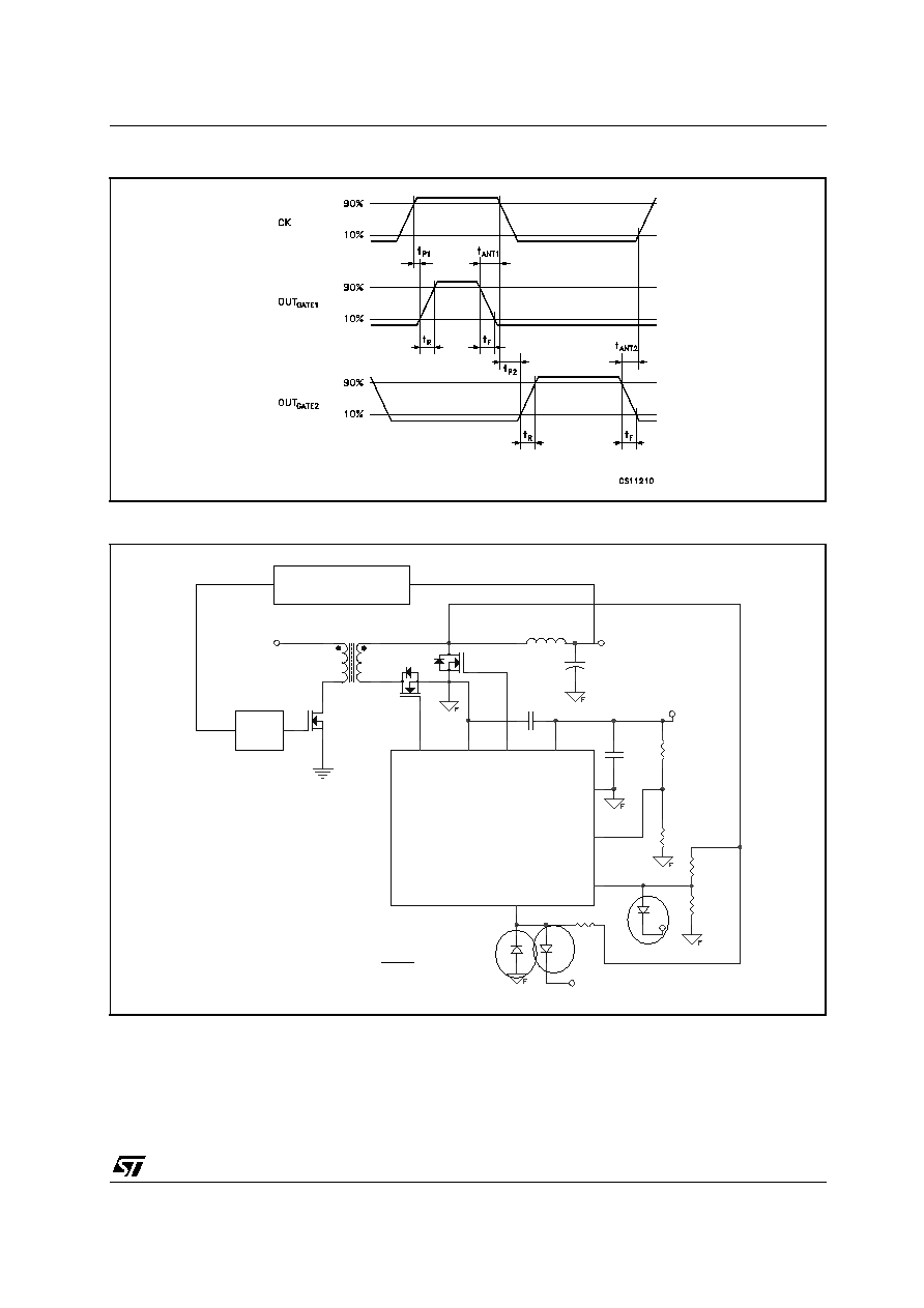
TIMING DIAGRAM
APPLICATION INFORMATION: STSR2 IN FORWARD CONVERTER SECONDARY SIDE
NOTES
1) Ceramic Capacitors C1 and C2 must be placed very close to the IC;
2) R1 and R2 set the anticipation time by partitioning the V
CC
voltage;
3) R3 and R4 is a resistor divider meant to provide the correct CK voltage range;
4) R5 limits the current flowing through diode D2 when Freewheeling drain voltage is high;
5) D1 could be necessary to protect INHIBIT pin from negative voltages.
6) D2 could be necessary to protect INHIBIT pin from voltages higher than V
CC
7) D3 could be necessary to protect CK pin from voltages higher than V
CC
.
8) SGLGND layout trace must not include OUT
GATE1,2
current paths.
9) A capacitor in parallel with R4 could be necessary to eliminate turn off voltage spike.
+5V
+5V
Vout
Vin
+5V
INDUCTOR
Cout
100nF
R1
R2
R3
R4
R5
D1
D2
100nF
TRANSFORMER
STSR2
4
5
1
8
2
6
3
7
Ck
I
NHI
B
I
T
O
U
T
G
at
e1
P
W
RG
ND
Vcc
SGLGND
SETANT
O
U
T
G
at
e2
MosfetN
Q1
MosfetN
Q2
D3
PWM
Feedback
Loop
option