 | –≠–ª–µ–∫—Ç—Ä–æ–Ω–Ω—ã–π –∫–æ–º–ø–æ–Ω–µ–Ω—Ç: STT4NF30L | –°–∫–∞—á–∞—Ç—å:  PDF PDF  ZIP ZIP |

STT4NF30L
N - CHANNEL 30V - 0.055
- 4A - TSOP-6
STripFET
TM
MOSFET
PRELIMINARY DATA
s
TYPICAL R
DS(on)
= 0.055
s
STANDARD OUTLINE FOR EASY
AUTOMATED SURFACE MOUNT ASSEMBLY
s
LOW THRESHOLD DRIVE
DESCRIPTION
This Power MOSFET is the latest development of
STMicroelectronics
unique
"Single
Feature
Size
TM
" strip-based process.The resulting transi-
stor shows extremely high packing density for low
on-resistance, rugged avalanche characteristics
and less critical alignment steps therefore a re-
markable manufacturing reproducibility.
APPLICATIONS
s
DC MOTOR DRIVE
s
DC-DC CONVERTERS
s
BATTERY MANAGEMENT IN NOMADIC
EQUIPMENT
s
POWER MANAGEMENT IN
PORTABLE/DESKTOP PCs
Æ
INTERNAL SCHEMATIC DIAGRAM
ABSOLUTE MAXIMUM RATINGS
Symbol
Parameter
Value
Un it
V
DS
Drain-source Voltage (V
GS
= 0)
30
V
V
DGR
Drain- gate Voltage (R
GS
= 20 k
)
30
V
V
GS
G ate-source Volt age
±
20
V
I
D
Drain Current (continuous) at T
c
= 25
o
C
4
A
I
D
Drain Current (continuous) at T
c
= 100
o
C
2.5
A
I
DM
(
∑
)
Drain Current (pulsed)
16
A
P
tot
T otal Dissipat ion at T
c
= 25
o
C
2
W
(
∑
) Pulse width limited by safe operating area
TYPE
V
DSS
R
DS(on)
I
D
STT4NF 30L
30 V
< 0.065
4 A
November 1998
TSOP-6
1/5
THERMAL DATA
R
thj -amb
T
J
T
s tg
(*)Thermal Resist ance Junction-ambient
Max
Maximum O perat ing Junction Temperature
Storage T emperature
62.5
150
-55 to 150
o
C/W
o
C
o
C
(*) Mounted on FR-4 board (t
5 sec)
ELECTRICAL CHARACTERISTICS (T
case
= 25
o
C unless otherwise specified)
OFF
Symbo l
Parameter
Test Con ditions
Min.
Typ.
Max.
Unit
V
(BR)DSS
Drain-source
Breakdown Voltage
I
D
= 250
µ
A
V
GS
= 0
30
V
I
DSS
Zero Gat e Voltage
Drain Current (V
GS
= 0)
V
DS
= Max Rat ing
V
DS
= Max Rat ing
T
c
= 125
o
C
1
10
µ
A
µ
A
I
G SS
Gat e-body Leakage
Current (V
DS
= 0)
V
GS
=
±
20 V
±
100
nA
ON (
)
Symbo l
Parameter
Test Con ditions
Min.
Typ.
Max.
Unit
V
G S(th)
Gat e Threshold Voltage V
DS
= V
GS
I
D
= 250
µ
A
1
1.7
2. 5
V
R
DS(on)
Static Drain-source On
Resistance
V
GS
= 10V
I
D
= 2 A
V
GS
= 4. 5V I
D
= 2 A
0.055
0.06
0.065
0.09
I
D(o n)
On State Drain Current
V
DS
> I
D(o n)
x R
DS(on )ma x
V
GS
= 10 V
4
A
DYNAMIC
Symbo l
Parameter
Test Con ditions
Min.
Typ.
Max.
Unit
g
f s
(
)
Forward
Transconductance
V
DS
> I
D(o n)
x R
DS(on )ma x
I
D
=6 A
6
S
C
iss
C
os s
C
rss
Input Capacitance
Out put Capacitance
Reverse Transfer
Capacitance
V
DS
= 25 V
f = 1 MHz
V
GS
= 0
420
62
20
550
80
30
pF
pF
pF
STT4NF30L
2/5
ELECTRICAL CHARACTERISTICS (continued)
SWITCHING ON
Symbo l
Parameter
Test Con ditions
Min.
Typ.
Max.
Unit
t
d(on)
t
r
Turn-on Time
Rise Time
V
DD
= 15 V
I
D
= 2 A
R
G
=4.7
V
GS
= 4.5 V
(see t est circuit, f igure 3)
13
30
17
40
ns
ns
Q
g
Q
gs
Q
gd
Tot al G ate Charge
Gat e-Source Charge
Gat e-Drain Charge
V
DD
= 24 V
I
D
= 4 A
V
GS
= 4.5 V
8
3.2
2.6
12
nC
nC
nC
SWITCHING OFF
Symbo l
Parameter
Test Con ditions
Min.
Typ.
Max.
Unit
t
r (Voff)
t
f
t
c
Off -volt age Rise T ime
Fall T ime
Cross-over Time
V
DD
= 24 V
I
D
= 4 A
R
G
=4.7
V
GS
= 4. 5 V
(see t est circuit, f igure 5)
6
9
20
8
12
26
ns
ns
ns
SOURCE DRAIN DIODE
Symbo l
Parameter
Test Con ditions
Min.
Typ.
Max.
Unit
I
SD
I
SDM
(
∑
)
Source-drain Current
Source-drain Current
(pulsed)
4
16
A
A
V
SD
(
)
Forward On Voltage
I
SD
= 4 A
V
GS
= 0
1. 2
V
t
rr
Q
rr
I
RRM
Reverse Recovery
Time
Reverse Recovery
Charge
Reverse Recovery
Current
I
SD
= 4 A
di/dt = 100 A/
µ
s
V
DD
= 15 V
T
j
= 150
o
C
(see t est circuit, f igure 5)
22
13
1.2
ns
nC
A
(
) Pulsed: Pulse duration = 300
µ
s, duty cycle 1.5 %
(
∑
) Pulse width limited by safe operating area
STT4NF30L
3/5
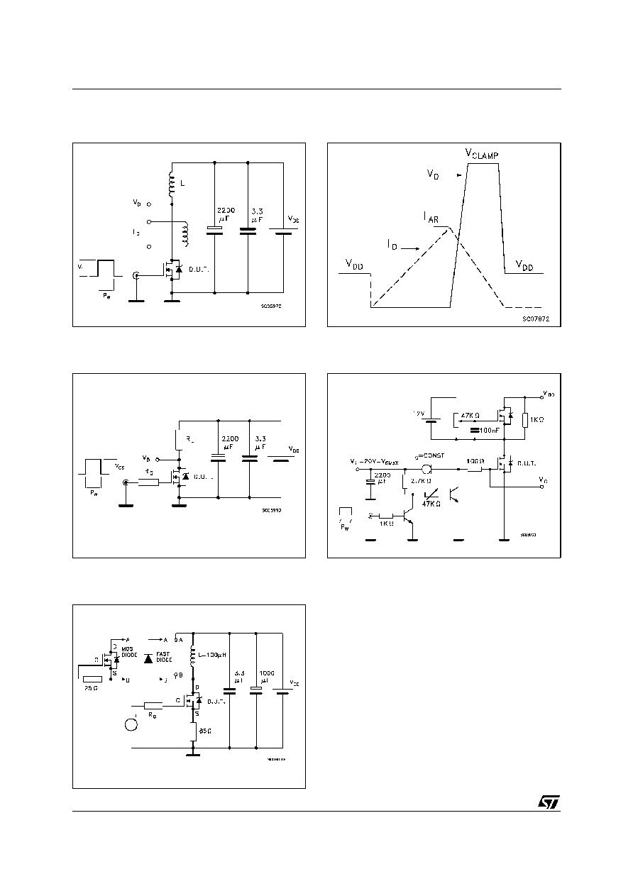
Fig. 1: Unclamped Inductive Load Test Circuit
Fig. 3: Switching Times Test Circuits For
Resistive Load
Fig. 2: Unclamped Inductive Waveform
Fig. 4: Gate Charge test Circuit
Fig. 5: Test Circuit For Inductive Load Switching
And Diode Recovery Times
STT4NF30L
4/5

Information furnished is believed to be accurate and reliable. However, STMicroelectronics assumes no responsibility for the consequences
of use of such information nor for any infringement of patents or other rights of third parties which may result from its use. No license is
granted by implication or otherwise under any patent or patent rights of STMicroelectronics. Specification mentioned in this publication are
subject to change without notice. This publication supersedes and replaces all information previously supplied. STMicroelectronics products
are not authorized for use as critical components in life support devices or systems without express written approval of STMicroelectronics.
The ST logo is a trademark of STMicroelectronics
©
1998 STMicroelectronics ≠ Printed in Italy ≠ All Rights Reserved
STMicroelectronics GROUP OF COMPANIES
Australia - Brazil - Canada - China - France - Germany - Italy - Japan - Korea - Malaysia - Malta - Mexico - Morocco - The Netherlands -
Singapore - Spain - Sweden - Switzerland - Taiwan - Thailand - United Kingdom - U.S.A.
http://www.st.com
.
STT4NF30L
5/5