STT818A
HIGH GAIN LOW VOLTAGE
PNP POWER TRANSISTOR
s
VERY LOW SATURATION VOLTAGE
s
DC CURRENT GAIN > 100 (h
FE
)
s
3 A CONTINUOUS COLLECTOR CURRENT
(I
C
)
s
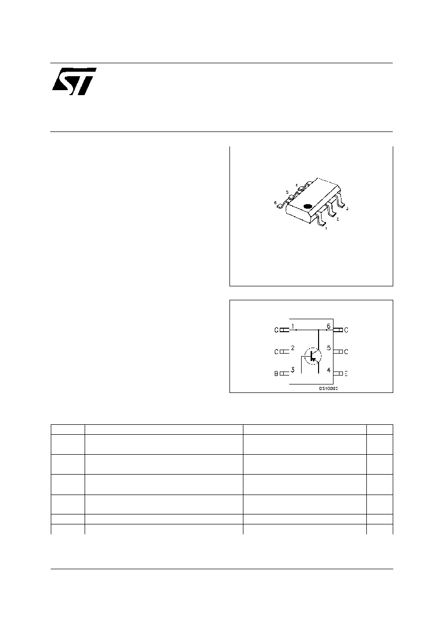
SURFACE-MOUNTING SOT23-6L PACKAGE
IN TAPE & REEL
APPLICATIONS
s
POWER MANAGEMENT IN PORTABLE
EQUIPMENTS
s
SWITCHING REGULATOR IN BATTERY
CHARGER APPLICATIONS
DESCRIPTION
Using the latest low voltage Epitaxial Planar
technology
based
on
interdigitated
layout,
STMicroelectronics has introduced the new "High
Gain"
Power bipolar
transistor family,
with
outstanding performances. Its very low saturation
voltage
combined
with
the
"high
gain"
characteristics make it ideal for all high efficiency
low voltage switching applications.
Marking : 818A
�
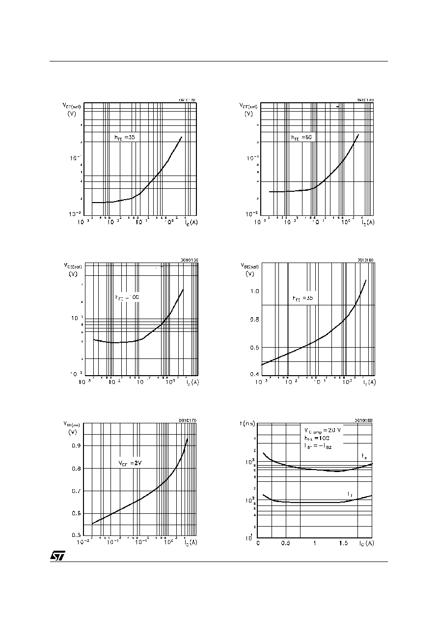
INTERNAL SCHEMATIC DIAGRAM
February 2001
SOT23-6L
(TSOP6)
ABSOLUTE MAXIMUM RATINGS
Symbol
Parameter
Val ue
Uni t
V
CBO
Collector-Base Voltage (I
E
= 0)
-30
V
V
CEO
Collector-Emit ter Voltage (I
B
= 0)
-30
V
V
EBO
Emitter-Base Voltage (I
C
= 0)
-5
V
I
C
Collector Current
-3
A
I
CM
Collector Peak Current
-6
A
I
B
Base Current
-0. 2
A
I
BM
Base Peak Current
-0. 5
A
P
t ot
Tot al Dissipation at T
C
= 25
o
C
1.2
W
T
stg
Storage Temperature
-65 to 150
o
C
T
j
Max. O perat ing Junction Temperature
150
o
C
1/6

THERMAL DATA
R
thj -am b
(1)
Thermal Resistance Junction-ambient
Max
105
o
C/W
(1) Package mounted on FR4 pcb 25mm x 25mm.
ELECTRICAL CHARACTERISTICS (T
case
= 25
o
C unless otherwise specified)
Symb ol
Parameter
Test Cond ition s
Mi n.
Typ .
Max.
Un it
I
CBO
Collect or Cut-off
Current (I
E
= 0)
V
CB
= -30 V
V
CB
= -30 V
T
C
= 125
o
C
-0.1
-20
�
A
�
A
I
EBO
Emitt er Cut-off Current
(I
C
= 0)
V
EB
= -5 V
-0.1
�
A
V
( BR)CEO
Collect or-Emitter
Breakdown Volt age
(I
B
= 0)
I
C
= -10 mA
-30
V
V
CE(sat )
Collect or-Emitter
Saturat ion Voltage
I
C
= -0.7 A
I
B
= -20 mA
I
C
= -1.2 A
I
B
= -20 mA
I
C
= -2 A
I
B
= -20 mA
-0.07
-0.12
-0.25
-0.12
-0.25
-0.5
V
V
V
V
BE(s at)
Base-Emitt er
Saturat ion Voltage
I
C
= -0.7 A
I
B
= -20 mA
-1.1
V
V
BE(ON)
Base-Emitt er Voltage
I
C
= -2 A
V
CE
= -2 V
-1.1
V
h
FE
DC Current G ain
I
C
= -0.5 A
V
CE
= -1 V
I
C
= -2.5 A
V
CE
= -3 V
100
100
300
Pulsed: Pulse duration = 300
�
s, duty cycle 1.5 %.
Safe Operating Area
DC Current Gain
STT818A
2/6
Collector Emitter Saturation Voltage
Collector Emitter Saturation Voltage
Base Emitter Voltage
Collector Emitter Saturation Voltage
Base Emitter Saturation Voltage
Switching Times Inductive Load
STT818A
3/6
Switching Times Resistive Load
Switching Times Resistive Load
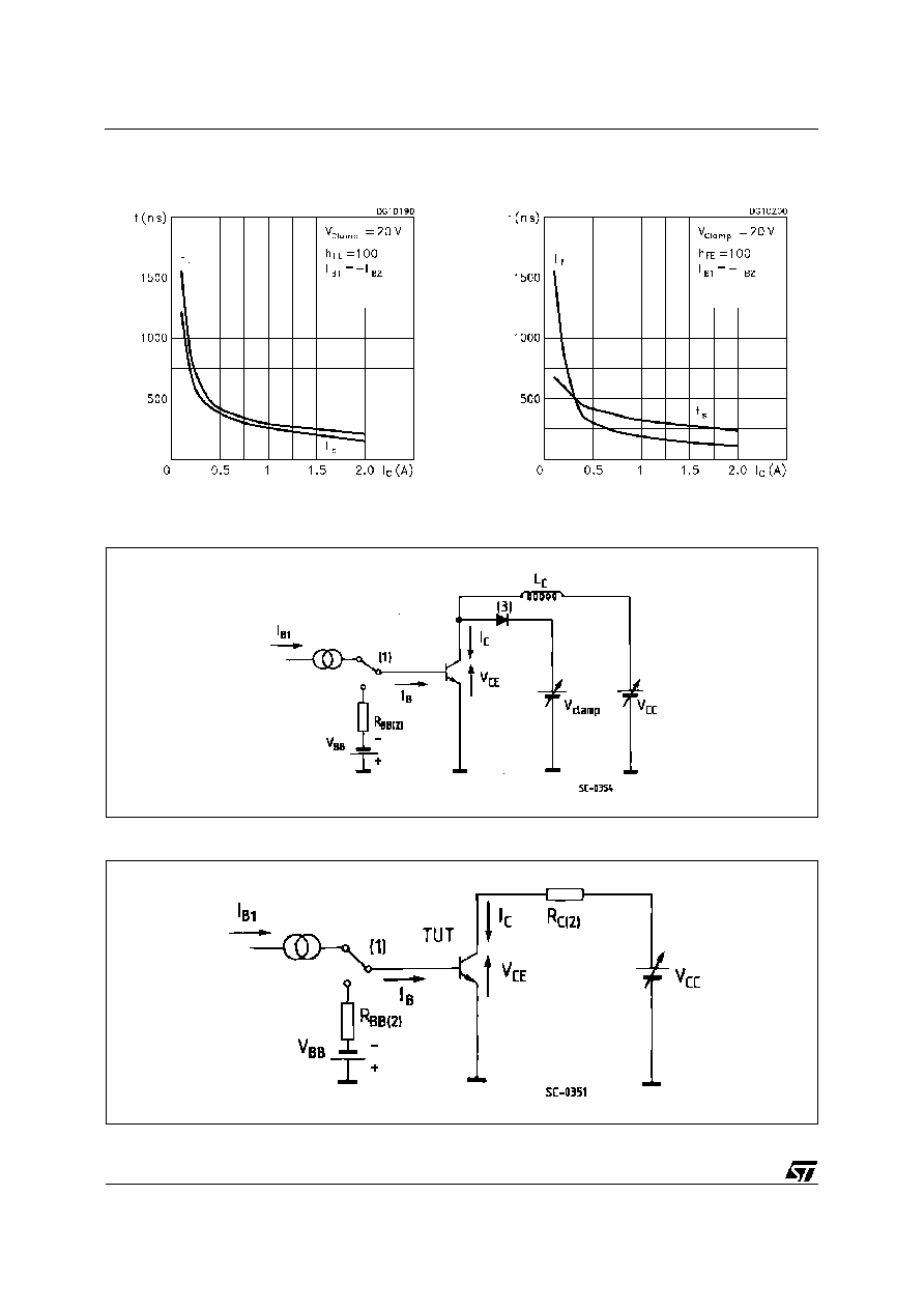
Figure 1: Inductive Load Switching Test Circuits.
Figure 2: Resistive Load Switching Test Circuits.
1) F ast elect ronic switch
2) Non-inductive Resistor
3) F ast recovery rectif ier
1) F ast elect ronic switch
2) Non-inductive Resistor
STT818A
4/6

DIM.
mm
mils
MIN.
TYP.
MAX.
MIN.
TYP.
MAX.
A
0.90
1.45
0.035
0.057
A1
0.00
0.15
0.000
0.006
A2
0.90
1.30
0.035
0.051
b
0.25
0.50
0.010
0.020
C
0.09
0.20
0.004
0.008
D
2.80
3.10
0.110
0.122
E
2.60
3.00
0.102
0.118
E1
1.50
1.75
0.059
0.069
L
0.35
0.55
0.014
0.022
e
0.95
0.037
e1
1.90
0.075
A A2
A1
b
e
e1
c
E
L
D
E1
SOT23-6L MECHANICAL DATA
STT818A
5/6