 | –≠–ª–µ–∫—Ç—Ä–æ–Ω–Ω—ã–π –∫–æ–º–ø–æ–Ω–µ–Ω—Ç: STT818B | –°–∫–∞—á–∞—Ç—å:  PDF PDF  ZIP ZIP |
STT818B
HIGH GAIN LOW VOLTAGE
PNP POWER TRANSISTOR
s
VERY LOW COLLECTOR TO EMITTER
SATURATION VOLTAGE
s
DC CURRENT GAIN > 100 (h
FE
)
s
3 A CONTINUOUS COLLECTOR CURRENT
(I
C
)
s
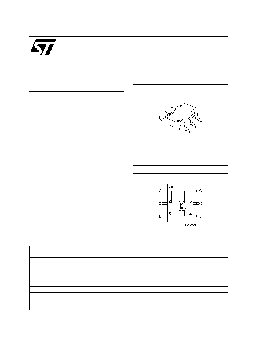
SURFACE-MOUNTING SOT23-6L PACKAGE
IN TAPE & REEL
APPLICATIONS
s
POWER MANAGEMENT IN PORTABLE
EQUIPMENTS
s
SWITCHING REGULATOR IN BATTERY
CHARGER APPLICATIONS
DESCRIPTION
The device is manufactured in low voltage PNP
Planar Technology by using a "Base Island"
layout.
The resulting Transistor shows exceptional high
gain performance coupled with very low
saturation voltage.
Æ
INTERNAL SCHEMATIC DIAGRAM
July 2002
SOT23-6L
(TSOP6)
ABSOLUTE MAXIMUM RATINGS
Symbol
Parameter
Value
Unit
V
CBO
Collector-Base Voltage (I
E
= 0)
-30
V
V
CEO
Collector-Emitter Voltage (I
B
= 0)
-30
V
V
EBO
Emitter-Base Voltage (I
C
= 0)
-5
V
I
C
Collector Current
-3
A
I
CM
Collector Peak Current
-6
A
I
B
Base Current
-0.2
A
I
BM
Base Peak Current
-0.5
A
P
tot
Total Dissipation at T
C
= 25
o
C
1.2
W
T
stg
Storage Temperature
-65 to 150
o
C
T
j
Max. Operating Junction Temperature
150
o
C
Type
Marking
STT818B
818B
1/5
THERMAL DATA
R
thj-amb
(1)
Thermal Resistance Junction-ambient Max
104.2
o
C/W
(1) Package mounted on FR4 pcb 25mm x 25mm.
ELECTRICAL CHARACTERISTICS (T
case
= 25
o
C unless otherwise specified)
Symbol
Parameter
Test Conditions
Min.
Typ.
Max.
Unit
I
CBO
Collector Cut-off
Current (I
E
= 0)
V
CB
= -30 V
V
CB
= -30 V T
C
= 125
o
C
-0.1
-20
µ
A
µ
A
I
EBO
Emitter Cut-off Current
(I
C
= 0)
V
EB
= -5 V
-0.1
µ
A
V
(BR)CEO
Collector-Emitter
Breakdown Voltage
(I
B
= 0)
I
C
= -10 mA
-30
V
V
CE(sat)
Collector-Emitter
Saturation Voltage
I
C
= -0.5 A I
B
= -5 mA
I
C
= -2 A I
B
= -20 mA
I
C
= -1.2 A I
B
= -20 mA
-0.075
-0.21
-0.15
-0.5
-0.25
V
V
V
V
BE(sat)
Base-Emitter
Saturation Voltage
I
C
= -0.5 A I
B
= -5 mA
I
C
= -1.2 A I
B
= -20 mA
I
C
= -2 A I
B
= -20 mA
-0.74
-1.1
-1.1
-1.2
V
V
V
V
BE(ON)
Base-Emitter Voltage
I
C
= -0.5 A V
CE
= -2 V
-0.71
-1.1
V
h
FE
DC Current Gain
I
C
= -0.5 A V
CE
= -1 V
I
C
= -2.5 A V
CE
= -3 V
100
100
* Pulsed: Pulse duration = 300
µ
s, duty cycle 1.5 %.
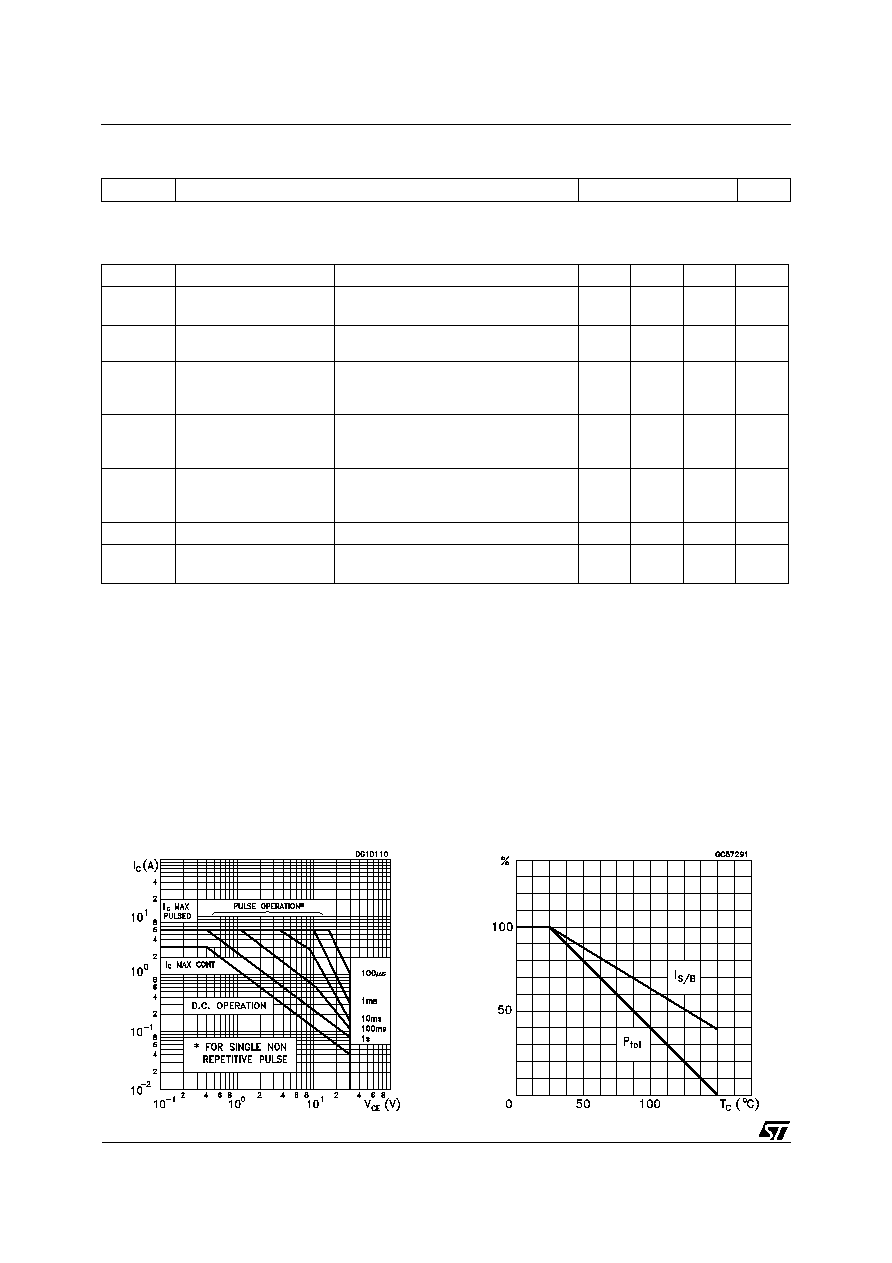
Safe Operating Area
Derating Curve
STT818B
2/5
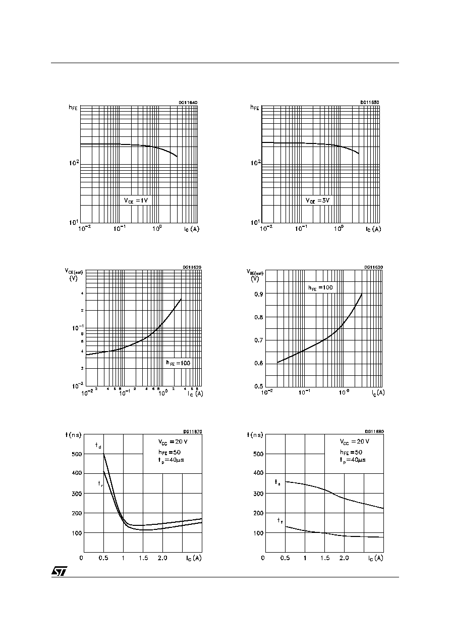
DC Current Gain
Collector-Emitter Saturation Voltage
Switching Times Resistive Load
DC Current Gain
Base-Emitter Saturation Voltage
Switching Times Resistive Load
STT818B
3/5

DIM.
mm
mils
MIN.
TYP.
MAX.
MIN.
TYP.
MAX.
A
0.90
1.45
0.035
0.057
A1
0.00
0.15
0.000
0.006
A2
0.90
1.30
0.035
0.051
b
0.25
0.50
0.010
0.020
C
0.09
0.20
0.004
0.008
D
2.80
3.10
0.110
0.122
E
2.60
3.00
0.102
0.118
E1
1.50
1.75
0.059
0.069
L
0.35
0.55
0.014
0.022
e
0.95
0.037
e1
1.90
0.075
A A2
A1
b
e
e1
c
E
L
D
E1
SOT23-6L MECHANICAL DATA
STT818B
4/5

Information furnished is believed to be accurate and reliable. However, STMicroelectronics assumes no responsibility for the consequences
of use of such information nor for any infringement of patents or other rights of third parties which may result from its use. No license is
granted by implication or otherwise under any patent or patent rights of STMicroelectronics. Specification mentioned in this publication are
subject to change without notice. This publication supersedes and replaces all information previously supplied. STMicroelectronics products
are not authorized for use as critical components in life support devices or systems without express written approval of STMicroelectronics.
The ST logo is a trademark of STMicroelectronics
© 2002 STMicroelectronics ≠ Printed in Italy ≠ All Rights Reserved
STMicroelectronics GROUP OF COMPANIES
Australia - Brazil - Canada - China - Finland - France - Germany - Hong Kong - India - Israel - Italy - Japan - Malaysia - Malta - Morocco -
Singapore - Spain - Sweden - Switzerland - United Kingdom - United States.
http://www.st.com
STT818B
5/5