 | –≠–ª–µ–∫—Ç—Ä–æ–Ω–Ω—ã–π –∫–æ–º–ø–æ–Ω–µ–Ω—Ç: STTA1206 | –°–∫–∞—á–∞—Ç—å:  PDF PDF  ZIP ZIP |

1/9
May 2002 - Ed: 5B
s
SPECIFIC
TO
"FREEWHEEL
MODE"
OPERATIONS: FREEWHEEL OR BOOSTER
DIODE.
s
ULTRA-FAST AND SOFT RECOVERY.
s
VERY LOW OVERALL POWER LOSSES IN
BOTH THE DIODE AND THE COMPANION
TRANSISTOR.
s
HIGH FREQUENCY OPERATIONS.
s
INSULATED PACKAGE : TO-220AC
Electrical insulation : 2500V
RMS
Capacitance < 7 pF
FEATURES AND BENEFITS
TURBOSWITCH, family, drastically cuts losses in
both the diode and the associated switching IGBT
or MOSFET in all "freewheel mode" operations
and is particularly suitable and efficient in motor
control freewheel applications and in booster
diode
applications
in
power
factor
control
circuitries.
Packaged in TO-220AC, isolated TO-220AC and
D
2
PAK, these 600V devices are particularly
intended for use on 240V domestic mains.
DESCRIPTION
I
F(AV)
12A
V
RRM
600V
t
rr
(typ)
28ns
V
F
(max)
1.5V
MAIN PRODUCT CHARACTERISTICS
Symbol
Parameter
Value
Unit
V
RRM
Repetitive peak reverse voltage
600
V
V
RSM
Non repetitive peak reverse voltage
600
V
I
F(RMS)
RMS forward current
TO-220AC / D2PAK
30
A
TO-220AC ins.
20
A
I
FRM
Repetitive peak
forward current
TO-220AC/D2PAK
tp=5
µ
s F=5kHz
square
160
A
TO-220AC ins.
120
A
I
FSM
Surge non repetitive forward current
tp=10 ms sinusoidal
110
A
T
j
Maximum operating junction temperature
150
∞C
T
stg
Storage temperature range
-65 to 150
∞C
TM : TURBOSWITCH is a trademark of STMicroelectronics
ABSOLUTE RATINGS (limiting values)
STTA1206D/DI/G
Æ
TURBOSWITCH ULTRA-FAST HIGH VOLTAGE DIODE
K
A
K
TO-220AC
STTA1206D
A
K
Insulated
TO-220AC
STTA1206DI
A
NC
K
D
2
PAK
STTA1206G

STTA1206D/DI/G
2/9
Symbol
Parameter
Test conditions
Min
Typ
Max
Unit
V
F *
Forward voltage drop
I
F
=12A
Tj = 25∞C
Tj = 125∞C
1.25
1.75
1.5
V
V
I
R **
Reverse leakage current
V
R
=0.8 x
V
RRM
Tj = 25∞C
Tj = 125∞C
2
100
5
µ
A
mA
V
to
Threshold voltage
Ip < 3.I
AV
Tj = 125∞C
1.15
V
rd
Dynamic resistance
29
m
Test pulse :
* tp = 380
µ
s,
cycle < 2%
** tp = 5 ms,
cycle < 2%
STATIC ELECTRICAL CHARACTERISTICS
Symbol
Parameter
Test conditions
Value
Unit
R
th(j-c)
Junction to case thermal
resistance
TO-220AC / D
2
PAK
TO-220AC ins.
1.9
3.0
∞C/W
P
1
Conduction power dissipation
I
F(AV)
= 12A
=0.5
TO-220AC / D
2
PAK
TO-220AC ins.
Tc= 108∞C
Tc= 84∞C
22
W
P
max
Total power dissipation
Pmax = P1 + P3
(P3 = 10% P1)
TO-220AC /D
2
PAK
TO-220AC ins.
Tc= 104∞C
Tc= 78∞C
24
W
THERMAL AND POWER DATA
Symbol
Parameter
Test conditions
Min
Typ
Max
Unit
t
rr
Reverse recovery
time
Tj = 25∞C
I
F
= 0.5 A
I
R
= 1A
Irr = 0.25A
I
F
= 1 A
dI
F
/dt =-50A/
µ
s V
R
=30V
28
55
ns
I
RM
Maximum reverse
recovery current
Tj = 125∞C VR = 400V
I
F
=12A
dI
F
/dt = -96 A/
µ
s
dI
F
/dt = -500 A/
µ
s
16
7.5
A
S factor
Softness factor
Tj = 125∞C V
R
= 400V
I
F
=12A
dI
F
/dt = -500 A/
µ
s
0.45
-
DYNAMIC ELECTRICAL CHARACTERISTICS
TURN-OFF SWITCHING
Symbol
Parameter
Test conditions
Min
Typ
Max
Unit
t
fr
Forward recovery
time
Tj = 25∞C
I
F
=12 A, dI
F
/dt = 96 A/
µ
s
measured at, 1.1
◊
V
F
max
500
ns
V
Fp
Peak forward voltage Tj = 25∞C
I
F
=12A, dI
F
/dt = 96 A/
µ
s
10
V
TURN-ON SWITCHING
To evaluate the maximum conduction losses use the following equation :
P = V
to
x I
F(AV)
+ rd x I
F
2
(RMS)

STTA1206D/DI/G
3/9
P1(W)
0
1
2
3
4
5
6
7
8
9
10
11
12
0
5
10
15
20
25
= 1
= 0.5
= 0.2
= 0.1
IF(av)(A)
T
=tp/T
tp
Fig. 1: Conduction losses versus average current.
0.1
1
10
100
200
0.00
0.25
0.50
0.75
1.00
1.25
1.50
1.75
2.00
2.25
2.50
2.75
3.00
VFM(V)
MAXIMUM VALUES
IFM(A)
Tj=125∞C
Fig. 2: Forward voltage drop versus forward
current.
1
0.8
K
0.6
0.4
0.2
0
K =
Zth(j-c) (tp. )
Rth(j-c)
Single pulse
= 0.1
= 0.2
= 0.5
1.0E-04
1.0E-03
1.0E-02
1.0E-01
1.0E+00
tp(s)
T
=tp/T
tp
Fig. 3: Relative variation of thermal transient
impedance junction to case versus pulse duration.
0
100
200
300
400
500
600
700
800
900 1000
0.0
2.5
5.0
7.5
10.0
12.5
15.0
17.5
20.0
22.5
25.0
27.5
30.0
32.5
35.0
37.5
40.0
IRM(A)
VR=400V
90% CONFIDENCE Tj=12∞ C
IF=12A
IF=6A
IF=24A
dIF/dt(A/µs)
Fig. 4: Peak reverse recovery current versus
dI
F
/dt.
0
100
200
300
400
500
600
700
800
900 1000
0
20
40
60
80
100
120
140
160
180
200
220
trr(ns)
VR=400V
90% CONFIDENCE Tj=125∞C
IF=12A
IF=6A
IF=24A
dIF/dt(A/µs)
Fig. 5: Reverse recovery time versus dI
F
/dt.
0
100
200
300
400
500
600
700
800
900 1000
0.0
0.1
0.2
0.3
0.4
0.5
0.6
0.7
0.8
0.9
1.0
1.1
1.2
S factor
VR=400V
IF<2xIF(av)
Typical values Tj=125∞C
dIF/dt(A/µs)
Fig. 6: Softness factor (tb/ta) versus dI
F
/dt.

STTA1206D/DI/G
4/9
0
25
50
75
100
125
150
0.50
0.75
1.00
1.25
1.50
1.75
2.00
IRM
S factor
Tj(∞C)
Fig. 7: Relative variation of dynamic parameters
versus junction temperature (Reference Tj=125∞C).
0
25
50
75
100
125
150
175
200
225
250
0
1
2
3
4
5
6
7
8
9
10
11
12
13
14
15
IF=IF(av)
VFP(V)
90% CONFIDENCE Tj=125∞C
dIF/dt(A/µs)
Fig. 8: Transient peak forward voltage versus
dI
F
/dt.
0
25
50
75
100
125
150
175
200
225
250
0
50
100
150
200
250
300
350
400
450
500
tfr(ns)
90% CONFIDENCE Tj=125∞C
VFr=1.1*VF max.
IF=IF(av)
dIF/dt(A/µs)
Fig. 9: Forward recovery time versus dI
F
/dt.
STTA1206D/DI/G
5/9
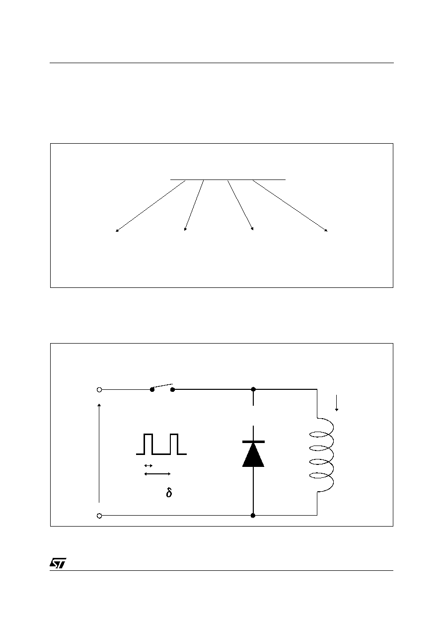
Fig. A : "FREEWHEEL" MODE.
TOTAL LOSSES
due to the diode
P = P1+ P2+ P3+ P4+ P5
Watts
SWITCHING
LOSSES
in the diode
SWITCHING
LOSSES
in the tansistor
due to the diode
CONDUCTION
LOSSES
in the diode
REVERSE
LOSSES
in the diode
The TURBOSWITCH is especially designed to
provide the lowest overall power losses in any
"FREEWHEEL
Mode"
application
(Fig.A)
considering both the diode and the companion
transistor, thus optimizing the overall performance
in the end application.
The way of calculating the power losses is given
below:
APPLICATION DATA
DIODE:
TURBOSWITCH
IL
LOAD
TRANSISTOR
SWITCHING
t
T
F = 1/T
= t/T
VR

STTA1206D/DI/G
6/9
Turn-on losses :
(in the transistor, due to the diode)
P5 =
V
I
S
F
x dI
dt
R
RM
F
◊
◊
+
◊
◊
2
3
2
6
(
)
+
◊
◊
◊
+
◊
V
I
I
S
F
x dI
dt
R
RM
L
F
(
)
2
2
Turn-off losses (in the diode) :
P3 =
V
I
S
F
x dI
dt
R
RM
F
◊
◊
◊
2
6
P3 and P5 are suitable for power MOSFET and
IGBT
I
I F
Rd
I R
V R
VtO
V F
V
Fig. B: STATIC CHARACTERISTICS
V
I
IL
t
TRANSISTOR
dI /dt
F
dI /dt
R
tb
ta
I RM
VR
DIODE
I
V
t
trr = ta + tb
S = tb / ta
Fig. C: TURN-OFF CHARACTERISTICS
I F
V F
V Fp
1.1V F
V F
F
dI /dt
0
0
t
t
I Fmax
tfr
Fig. D: TURN-ON CHARACTERISTICS
Conduction losses :
P1 = V
t0
. I
F(AV)
+ R
d
. I
F
2
(RMS)
Reverse losses :
P2 = V
R
. I
R
. (1 -
)
Turn-on losses :
P4 = 0.4 (V
FP
- V
F
) . I
Fmax
. t
fr
. F
APPLICATION DATA (Cont'd)
STTA1206D/DI/G
7/9
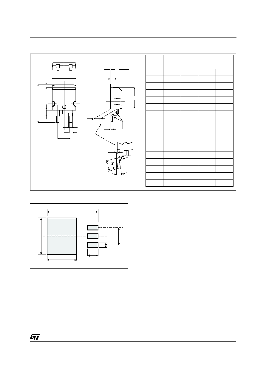
PACKAGE DATA
D2PAK
REF.
DIMENSIONS
Millimeters
Inches
Min.
Max.
Min.
Max.
A
4.40
4.60
0.173
0.181
A1
2.49
2.69
0.098
0.106
A2
0.03
0.23
0.001
0.009
B
0.70
0.93
0.027
0.037
B2
1.14
1.70
0.045
0.067
C
0.45
0.60
0.017
0.024
C2
1.23
1.36
0.048
0.054
D
8.95
9.35
0.352
0.368
E
10.00
10.40
0.393
0.409
G
4.88
5.28
0.192
0.208
L
15.00
15.85
0.590
0.624
L2
1.27
1.40
0.050
0.055
L3
1.40
1.75
0.055
0.069
M
2.40
3.20
0.094
0.126
R
0.40 typ.
0.016 typ.
V2
0∞
8∞
0∞
8∞
A
C2
D
R
A2
M
V2
C
A1
G
L
L3
L2
B
B2
E
*
* FLAT ZONE NO LESS THAN 2mm
8.90
3.70
1.30
5.08
16.90
10.30
FOOTPRINT DIMENSIONS (in millimeters)
STTA1206D/DI/G
8/9
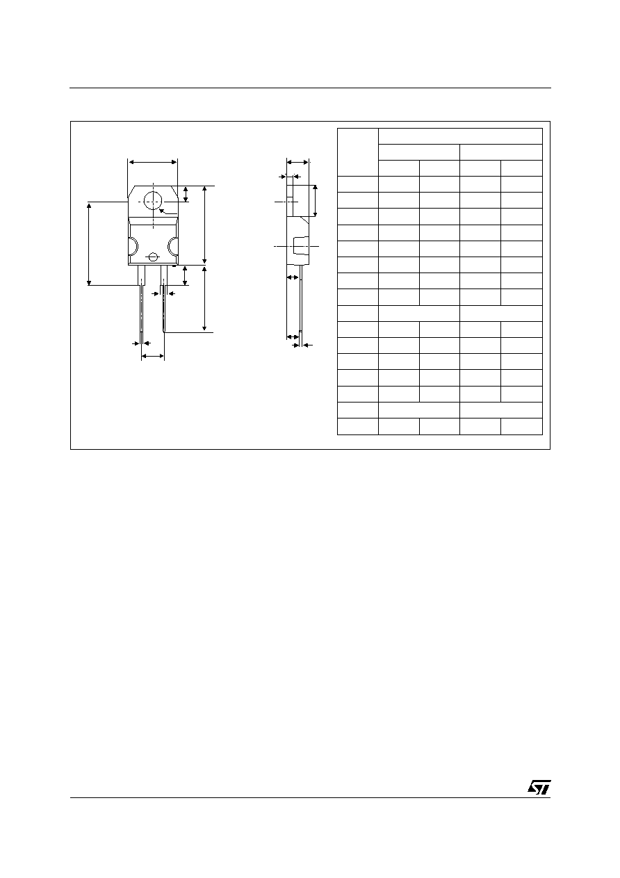
s
Cooling method : by conduction (C)
s
Recommanded maximum torque value : 0.7m.N
PACKAGE DATA
TO-220AC (JEDEC outline)
REF.
DIMENSIONS
Millimeters
Inches
Min.
Max.
Min.
Max.
A
4.40
4.60
0.173
0.181
C
1.23
1.32
0.048
0.051
D
2.40
2.72
0.094
0.107
E
0.49
0.70
0.019
0.027
F
0.61
0.88
0.024
0.034
F1
1.14
1.70
0.044
0.066
G
4.95
5.15
0.194
0.202
H2
10.00
10.40
0.393
0.409
L2
16.40 typ.
0.645 typ.
L4
13.00
14.00
0.511
0.551
L5
2.65
2.95
0.104
0.116
L6
15.25
15.75
0.600
0.620
L7
6.20
6.60
0.244
0.259
L9
3.50
3.93
0.137
0.154
M
2.6 typ.
0.102 typ.
Diam. I
3.75
3.85
0.147
0.151
A
C
D
E
M
L7
H2
ÿ I
L5
L6
L9
L4
G
F1
F
L2
STTA1206D/DI/G
9/9
PACKAGE DATA
INSULATED TO-220AC (JEDEC outline)
REF.
DIMENSIONS
Millimeters
Inches
Min. Typ. Max. Min. Typ. Max.
A
15.20
15.90 0.598
0.625
a1
3.75
0.147
a2
13.00
14.00 0.511
0.551
B
10.00
10.40 0.393
0.409
b1
0.61
0.88 0.024
0.034
b2
1.23
1.32 0.048
0.051
C
4.40
4.60 0.173
0.181
c1
0.49
0.70 0.019
0.027
c2
2.40
2.72 0.094
0.107
e
4.80
5.40 0.189
0.212
F
6.20
6.60 0.244
0.259
I
3.75
3.85 0.147
0.151
I4
15.80 16.40 16.80 0.622 0.646 0.661
L
2.65
2.95 0.104
0.116
l2
1.14
1.70 0.044
0.066
M
2.60
0.102
Cooling method : by conduction (C).
Recommended maximum torque value : 1 m.N
M
B
l4
C
b2
a2
l2
c2
b1
a1
A
F
L
I
e
c1
Information furnished is believed to be accurate and reliable. However, STMicroelectronics assumes no responsibility for the consequences of
use of such information nor for any infringement of patents or other rights of third parties which may result from its use. No license is granted by
implication or otherwise under any patent or patent rights of STMicroelectronics. Specifications mentioned in this publication are subject to
change without notice. This publication supersedes and replaces all information previously supplied.
STMicroelectronics products are not authorized for use as critical components in life support devices or systems without express written ap-
proval of STMicroelectronics.
The ST logo is a registered trademark of STMicroelectronics
© 2002 STMicroelectronics - Printed in Italy - All rights reserved.
STMicroelectronics GROUP OF COMPANIES
Australia - Brazil - Canada - China - Finland - France - Germany
Hong Kong - India - Israel - Italy - Japan - Malaysia - Malta - Morocco - Singapore
Spain - Sweden - Switzerland - United Kingdom - United States.
http://www.st.com
Ordering type
Marking
Package
Weight
Base qty
Delivery mode
STTA1206D
STTA1206D
TO-220AC
1.86g
50
Tube
STTA1206DI
STTA1206DI
TO-220AC Ins.
1.86g
250
Bulk
STTA1206G
STTA1206G
D
2
PAK
1.48g
50
Tube
STTA1206G-TR
STTA1206G
D
2
PAK
1.48g
500
Tape & reel
s
Epoxy meets UL94,V0