TURBOSWITCH is a trademark of STMicroelectronics
November 1999 - Ed: 4A
SPECIFIC TO THE FOLLOWING OPERATIONS:
SNUBBING OR CLAMPING, DEMAGHETIZATION
AND RECTIFICATION
ULTRA-FAST AND SOFT RECOVERY
VERY LOW OVERALL POWER LOSSES IN
BOTH THE DIODE AND THE COMPANION
TRANSISTOR
HIGH FREQUENCY OPERATION
HIGH REVERSE VOLTAGE CAPABILITY
FEATURES AND BENEFITS
TURBOSWITCH 1200V drastically cuts losses in
all high voltage operations which require extremely
fast, soft and noise-free power diodes.
Due to their optimized switching performances
they aloso highly decrease power losses in any
associated switching IGBT or MOSFET in all
"freewheel mode" operations and is particulary
suitable and efficient in motor control circuitries, or
in primary of SMPS as snubber, clamping or
demagnetizing diodes secondary of SMPS as high
voltage rectifier diodes. They are also suitable for
the secondary of SMPS as high voltage rectifier
diodes.
DESCRIPTION
I
F(AV)
2A
V
RRM
1200V
t
rr
(typ)
65ns
V
F
(max)
1.5V
MAIN PRODUCT CHARACTERISTICS
Symbol
Parameter
Value
Unit
V
RRM
Repetitive peak reverse voltage
1200
V
V
RSM
Non repetitive peak reverse voltage
1200
V
I
F(RMS)
RMS forward current
10
A
I
FRM
Repetitive peak forward current
tp = 5
µ
s F=5kHz square
20
A
I
FSM
Surge non repetitive forward current
tp = 10ms sinusoidal
25
A
T
stg
Storage temperature range
- 65 to + 150
∞C
T
j
Maximum operating junction temperature
125
∞C
ABSOLUTE RATINGS (limiting values)
STTA212S
Æ
TURBOSWITCH
TM
ULTRA-FAST HIGH VOLTAGE DIODE
SMC
1/8

Symbol
Parameter
Test Conditions
Min
Typ
Max
Unit
V
F *
Forward voltage drop
I
F
= 2A
Tj = 25∞C
Tj = 125∞C
1.1
1.65
1.5
V
I
R **
Reverse leakage current
V
R
= 0.8
x V
RRM
Tj = 25∞C
Tj = 125∞C
150
20
400
µ
A
Vto
Threshold voltage
Ip < 3.I
AV
Tj = 125∞C
1.15
V
rd
Dynamic resistance
175
m
Test pulses :
* tp = 380
µ
s,
< 2%
** tp = 5 ms ,
< 2%
STATIC ELECTRICAL CHARACTERISTICS
Symbol
Parameter
Test conditions
Value
Unit
R
th(j-I)
Junction to lead thermal resistance
21
∞C/W
P
1
Conduction power dissipation
I
F(AV)
= 1.5A
= 0.5
Tlead= 72∞C
2.5
W
P
max
Total power dissipation
Pmax = P1 + P3 (P3 = 10% P1)
Tlead= 67∞C
2.8
W
THERMAL AND POWER DATA
Symbol
Parameter
Test conditions
Min
Typ
Max
Unit
t
rr
Reverse recovery
time
Tj = 25∞C
I
F
= 0.5 A I
R
= 1A Irr = 0.25A
I
F
= 1 A dI
F
/dt =-50A/
µ
s V
R
= 30V
65
115
ns
I
RM
Maximum recovery
current
Tj = 125∞C V
R
= 600V I
F
= 2A
dI
F
/dt = -16 A/
µ
s
dI
F
/dt = -50 A/
µ
s
6.0
3.6
A
S factor
Softness factor
Tj = 125∞C V
R
= 600V I
F
= 2A
dI
F
/dt = -50 A/
µ
s
0.9
/
DYNAMIC ELECTRICAL CHARACTERISTICS
TURN-OFF SWITCHING
Symbol
Parameter
Test conditions
Min
Typ
Max
Unit
t
fr
Forward recovery time
Tj = 25∞C
I
F
= 2 A
dI
F
/dt = 16 A/
µ
s
measured at 1.1
◊
V
F
max
900
ns
V
Fp
Peak forward voltage
35
V
TURN-ON SWITCHING
To evaluate the maximum conduction losses use the following equation :
P = V
to
x I
F(AV)
+ rd x I
F
2
(RMS)
STTA212S
2/8
0.0
0.2
0.4
0.6
0.8
1.0
1.2
1.4
1.6
1.8
2.0
0.0
0.5
1.0
1.5
2.0
2.5
3.0
P1(W)
=0.1
=0.2
=0.5
=1
IF(av) (A)
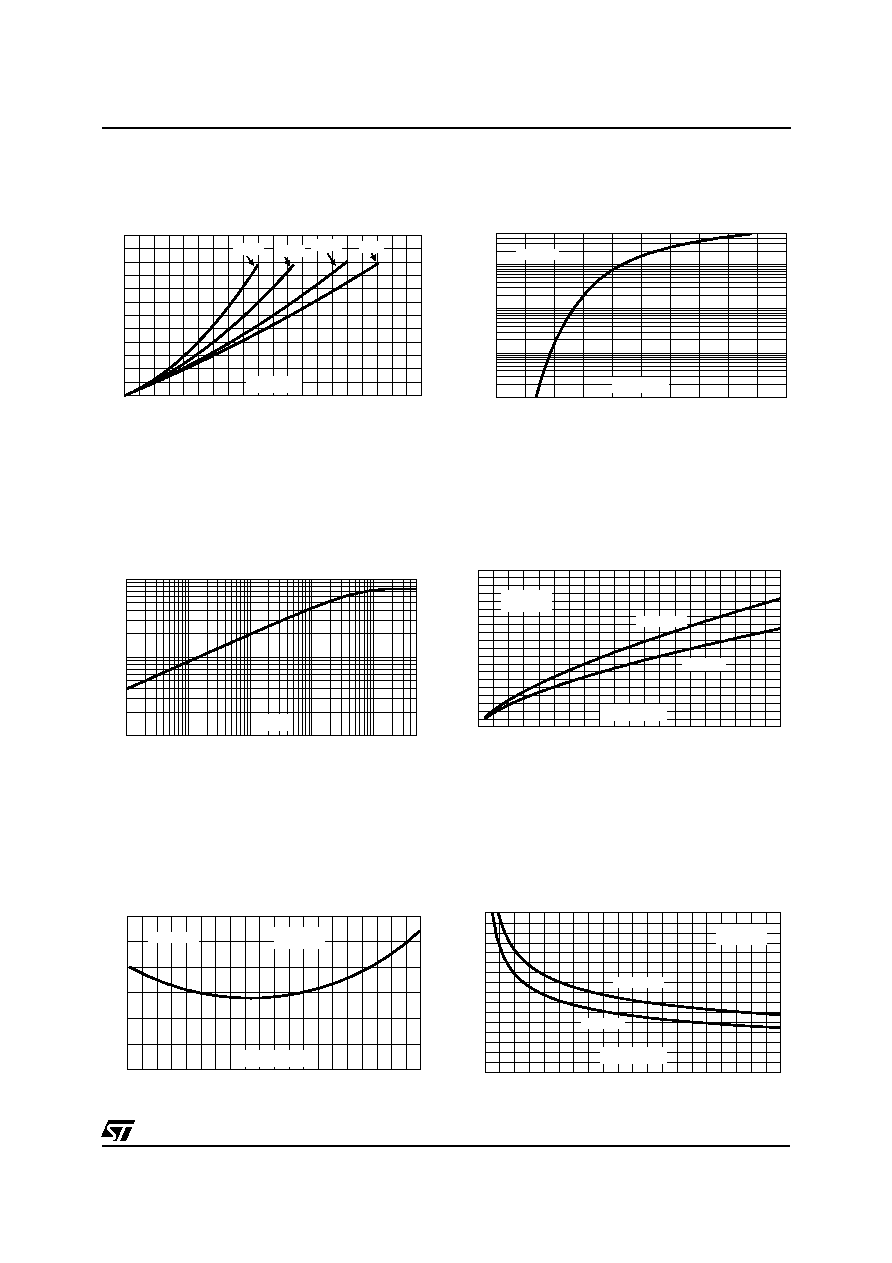
Fig. 1: Conduction losses versus average current.
0
1
2
3
4
5
1E-2
1E-1
1E+0
1E+1
5E+1
IFM(A)
Tj=125∞C
VFM(V)
Fig. 2: Forward voltage drop versus forward
current (maximum values).
1E-1
1E+0
1E+1
1E+2
tp(s)
Zth(j-a)(∞C/W)
1E-2
5E+2
1
10
100
Fig. 3: Variation of thermal impedance junction to
ambient versus pulse duration (epoxy printed cir-
cuit board FR4, e(Cu)=35
µ
m, S(Cu)=1cm2).
0
20
40
60
80
100
120
140
160
180
200
0.60
0.80
1.00
1.20
S factor
VR=600V
Tj=125∞C
IF<2*IF(av)
dIF/dt(A/µs)
Fig. 5: Softness factor (tb/ta) versus dI
F
/dt (typical
values).
0
20
40
60
80
100
120
140
160
180
200
0
50
100
150
200
250
300
350
400
trr(ns)
VR=600V
Tj=125∞C
IF=2*IF(av)
IF=IF(av)
dIF/dt(A/µs)
Fig. 6: Reverse recovery time versus dI
F
/dt (90%
confidence).
0
20
40
60
80
100
120
140
160
180
200
0
5
10
15
20
IRM(A)
VR=600V
Tj=125∞C
IF=2*IF(av)
IF=IF(av)
dIF/dt(A/µs)
Fig. 4: Peak reverse recovery current versus dI
F
/dt
(90% confidence).
STTA212S
3/8
0
20
40
60
80
100
0
10
20
30
40
50
60
VFP(V)
Tj=125∞C
IF=IF(av)
dIF/dt(A/µs)
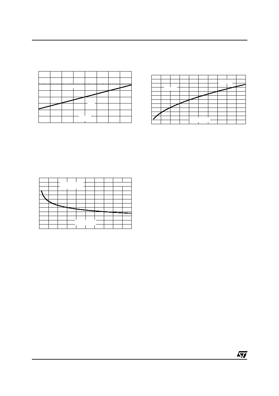
Fig. 8: Transient peak forward voltage versus
dI
F
/dt.
0
20
40
60
80
100
200
300
400
500
600
700
800
tfr(ns)
Tj=125∞C
VFR=1.1*VF max.
IF=IF(av)
dIF/dt(A/µs)
Fig. 9: Forward recovery time versus dI
F
/dt.
25
50
75
100
125
0.7
0.8
0.9
1.0
1.1
IRM
S factor
Tj(∞C)
Fig. 7: Relative variation of dynamic parameters
versus junction temperature (reference Tj=125∞C).
STTA212S
4/8
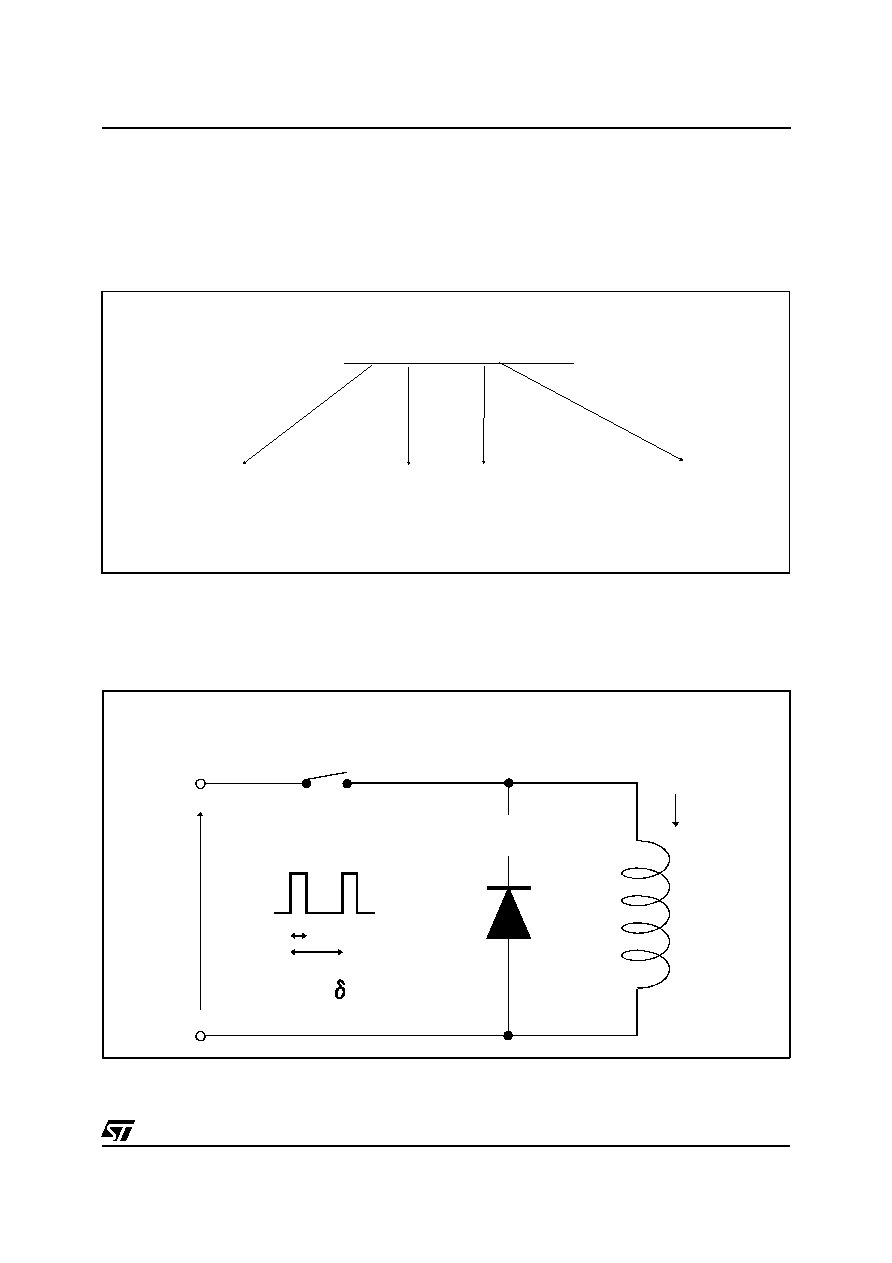
TOTAL LOSSES
due to the diode
P = P1+ P2+ P3+ P4+ P5 Watts
SWITCHING
LOSSES
in the diode
CONDUCTION
LOSSES
in the diode
SWITCHING
LOSSES
in the transistor
due to the diode
REVERSE
LOSSES
in the diode
The 1200V TURBOSWITCH has been designed
to provide the lowest overall power losses in any all
high frequency or high pulsed current operations.
In such applications (fig. A to D), the way of
calculating the power losses is given below :
APPLICATION DATA
Fig. A : "FREEWHEEL" MODE
DIODE:
TURBOSWITCH
IL
LOAD
TRANSISTOR
SWITCHING
t
T
F = 1/T
= t/T
VR
STTA212S
5/8