Æ
1/8
Table 1: Main Product Characteristics
I
F(AV)
Up to 2 x 10 A
V
RRM
600 V
T
j
175∞C
V
F
(typ)
1.05 V
t
rr
(max)
35 ns
STTH16L06C
TURBO 2 ULTRAFAST HIGH VOLTAGE RECTIFIER
Table 3: Absolute Ratings (limiting values, per diode)
Symbol
Parameter
Value
Unit
V
RRM
Repetitive peak reverse voltage
600
V
I
F(RMS)
RMS forward voltage
30
A
I
F(AV)
Average forward
current
= 0.5
TO-220AB / D
2
PAK
Tc = 140∞C
Tc = 135∞C
Tc = 130∞C
Tc = 120∞C
Per diode
Per device
Per diode
Per device
8
16
10
20
A
TO-220FPAB
Tc = 110∞C
Tc = 80∞C
Per diode
Per device
8
16
I
FSM
Surge non repetitive forward current
tp = 10ms sinusoidal
90
A
T
stg
Storage temperature range
-65 to + 175
∞C
T
j
Maximum operating junction temperature
175
∞C
K
A2
A1
TO-220AB
STTH16L06CT
K
A2
A1
TO-220FPAB
STTH16L06CFP
K
A2
A1
D
2
PAK
STTH16L06CG
K
A1
A2
September 2004
REV. 1
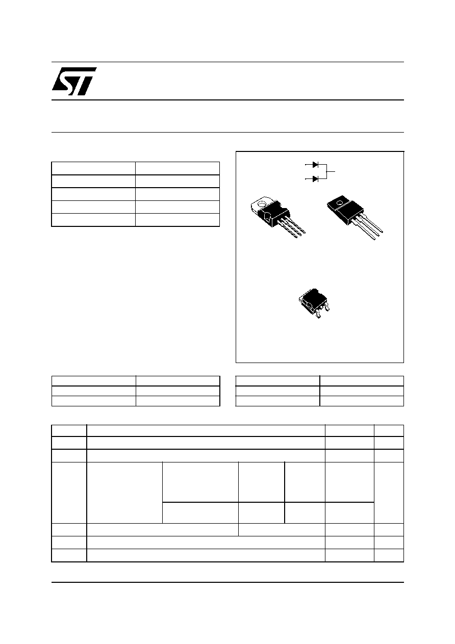
FEATURES AND BENEFITS
Ultrafast switching
Low reverse recovery current
Low thermal resistance
Reduces switching & conduction losses
DESCRIPTION
The STTH16L06, which is using ST Turbo 2 600V
technology, is specially suited for use in switching
power supplies, and industrial applications, as
rectification and discontinuous mode PFC boost
diode.
Table 2: Order Codes
Part Number
Marking
STTH16L06CT
STTH16L06CT
STTH16L06CFP
STTH16L06CFP
.
Part Number
Marking
STTH16L06CG
STTH16L06CG
STTH16L06GG-TR
STTH16L06CG

STTH16L06C
2/8
Table 4: Thermal Resistance
Table 5: Static Electrical Characteristics
Pulse test:
* tp = 5 ms,
< 2%
** tp = 380 µs,
< 2%
To evaluate the conduction losses use the following equation: P = 1.06 x I
F(AV)
+ 0.036 I
F
2
(RMS)
Table 6: Dynamic Characteristics (per diode)
Symbol
Parameter
Value (max).
Unit
R
th(j-c)
Junction to case
TO-220AB / D
2
PAK
Per diode
2.5
∞C/W
TO-220FPAB
Per diode
5
TO-220AB / D
2
PAK
Total
1.6
TO-220FPAB
Total
3.8
R
th(c)
Coupling
TO-220AB / D
2
PAK
0.7
∞C/W
TO-220FPAB
2.5
When the diodes 1 and 2 are used simultaneously:
Tj(diode 1) = P(diode 1) x R
th(j-c)
(Per diode) + P(diode 2) x R
th(c)
Symbol
Parameter
Test conditions
Min.
Typ
Max.
Unit
I
R
*
Reverse leakage current T
j
= 25∞C
V
R
= V
RRM
8
µA
T
j
= 150∞C
25
240
V
F
**
Forward voltage drop
T
j
= 25∞C
I
F
= 8A
1.8
V
T
j
= 150∞C
1.05
1.35
T
j
= 25∞C
I
F
= 16A
2.08
T
j
= 150∞C
1.28
1.64
Symbol
Parameter
Test conditions
Min.
Typ Max.
Unit
t
rr
Reverse recovery
time
T
j
= 25∞C
I
F
= 0.5A Irr = 0.25A I
R
=1A
35
ns
I
F
= 1A dI
F
/dt = 50 A/µs V
R
=30V
40
55
I
RM
Reverse recovery
current
T
j
= 125∞C I
F
= 8A V
R
= 400V
dI
F
/dt = 100 A/µs
4.5
6.5
A
t
fr
Forward recovery
time
T
j
= 25∞C
I
F
= 8A dI
F
/dt = 100 A/µs
V
FR
= 1.1 x V
Fmax
200
ns
V
FP
Forward recovery
voltage
T
j
= 25∞C
I
F
= 8A dI
F
/dt = 100 A/µs
V
FR
= 1.1 x V
Fmax
3.5
V
STTH16L06C
3/8
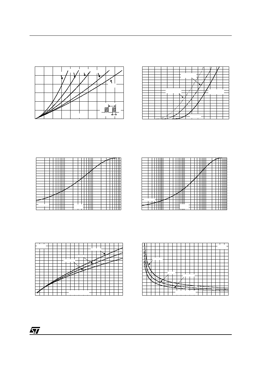
Figure 1: Conduction losses versus average
forward current (per diode)
Figure 2: Forward voltage drop versus forward
current (per diode)
Figure 3: Relative variation of thermal
impedance junction to case versus pulse
duration (TO-220AB & D
2
PAK)
Figure 4: Relative variation of thermal
impedance junction to case versus pulse
duration (TO-220FPAB)
Figure 5: Peak reverse recovery current versus
dI
F
/dt (typical values, per diode)
Figure 6: Reverse recovery time versus dI
F
/dt
(typical values, per diode)
0
5
10
15
0
2
4
6
8
10
P(W)
T
=tp/T
tp
= 0.05
= 1
I
(A)
F(AV)
= 0.1 = 0.2
= 0.5
0
10
20
30
40
50
60
70
80
90
100
0.0
0.5
1.0
1.5
2.0
2.5
3.0
3.5
I
(A)
FM
T =150∞C
(typical values)
j
T =25∞C
(maximum values)
j
T =150∞C
(maximum values)
j
V
(V)
FM
0.0
0.1
0.2
0.3
0.4
0.5
0.6
0.7
0.8
0.9
1.0
1.E-03
1.E-02
1.E-01
1.E+00
Z
/R
th(j-c)
th(j-c)
t (s)
p
Single pulse
0.0
0.1
0.2
0.3
0.4
0.5
0.6
0.7
0.8
0.9
1.0
1.E-03
1.E-02
1.E-01
1.E+00
1.E+01
Z
/R
th(j-c)
th(j-c)
t (s)
p
Single pulse
0
2
4
6
8
10
12
14
16
18
0
50
100
150
200
250
300
350
400
450
500
I
(A)
RM
dI /dt(A/µs)
F
I =2 x I
F
F(AV)
I =I
F
F(AV)
I =0.5 x I
F
F(AV)
V =400V
T =125∞C
R
j
0
50
100
150
200
250
300
350
400
0
50
100
150
200
250
300
350
400
450
500
t (ns)
rr
dI /dt(A/µs)
F
I =I
F
F(AV)
I =0.5 x I
F
F(AV)
V =400V
T =125∞C
R
j
I =2 x I
F
F(AV)
STTH16L06C
4/8
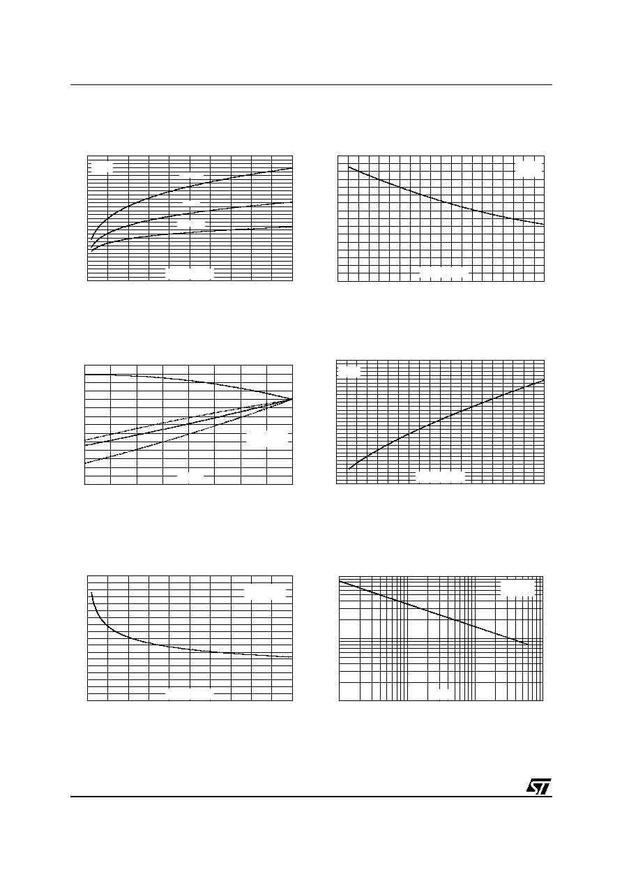
Figure 7: Reverse recovery charges versus
dI
F
/dt (typical values, per diode)
Figure 8: Reverse recovery softness factor
versus dI
F
/dt (typical values, per diode)
Figure 9: Relative variations of dynamic
parameters versus junction temperature
Figure 10: Transient peak forward voltage
versus dI
F
/dt (typical values, per diode)
Figure 11: Forward recovery time versus dI
F
/dt
(typical values, per diode)
Figure 12: Junction capacitance versus
reverse voltage applied (typical values, per
diode)
0
50
100
150
200
250
300
350
400
450
500
550
600
650
700
750
800
0
100
200
300
400
500
Q (nC)
rr
I =2 x I
F
F(AV)
I =I
F
F(AV)
I =0.5 x I
F
F(AV)
V =400V
T =125∞C
R
j
dI /dt(A/µs)
F
0.0
0.2
0.4
0.6
0.8
1.0
1.2
1.4
1.6
0
50
100
150
200
250
300
350
400
450
500
S factor
dI /dt(A/µs)
F
I < 2 x I
T =125∞C
F
F(AV)
j
V =400V
R
0.0
0.2
0.4
0.6
0.8
1.0
1.2
1.4
25
50
75
100
125
I
RM
Q
RR
t
rr
S factor
T (∞C)
j
I =I
Reference: T =125∞C
F
F(AV)
j
V =400V
R
0
1
2
3
4
5
6
7
8
9
10
11
12
13
14
15
16
0
50
100
150
200
250
300
350
400
450
500
V
(V)
FP
dI /dt(A/µs)
F
I =I
T =125∞C
F
F(AV)
j
0
20
40
60
80
100
120
140
160
180
0
100
200
300
400
500
t (ns)
fr
dI /dt(A/µs)
F
I =I
T =125∞C
F
F(AV)
j
V
=1.1 x V max.
FR
F
1
10
100
1
10
100
1000
C(pF)
V (V)
R
F=1MHz
V
=30mV
T =25∞C
OSC
RMS
j
STTH16L06C
5/8
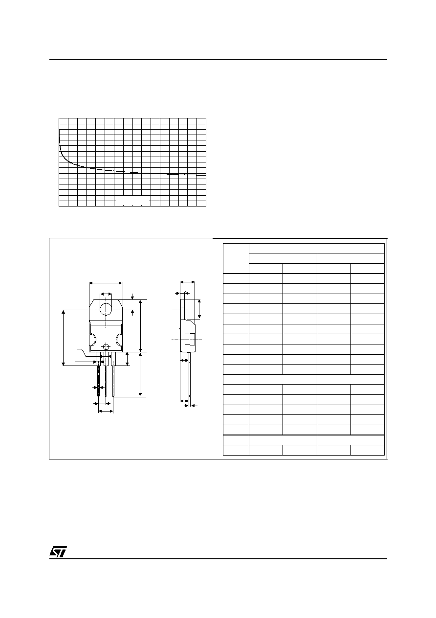
Figure 14: TO-220AB Package Mechanical Data
Figure 13: Thermal resistance junction to
ambient versus copper surface under tab
(epoxy FR4, e
CU
=35µm) (D
2
PAK)
0
10
20
30
40
50
60
70
80
0
5
10
15
20
25
30
35
40
R
(∞C/W)
th(j-a)
S
(cm≤)
CU
A
C
D
L7
Dia
L5
L6
L9
L4
F
H2
G
G1
L2
F2
F1
E
M
REF.
DIMENSIONS
Millimeters
Inches
Min.
Max.
Min.
Max.
A
4.40
4.60
0.173
0.181
C
1.23
1.32
0.048
0.051
D
2.40
2.72
0.094
0.107
E
0.49
0.70
0.019
0.027
F
0.61
0.88
0.024
0.034
F1
1.14
1.70
0.044
0.066
F2
1.14
1.70
0.044
0.066
G
4.95
5.15
0.194
0.202
G1
2.40
2.70
0.094
0.106
H2
10
10.40
0.393
0.409
L2
16.4 typ.
0.645 typ.
L4
13
14
0.511
0.551
L5
2.65
2.95
0.104
0.116
L6
15.25
15.75
0.600
0.620
L7
6.20
6.60
0.244
0.259
L9
3.50
3.93
0.137
0.154
M
2.6 typ.
0.102 typ.
Diam.
3.75
3.85
0.147
0.151