 | ÐлекÑÑоннÑй компоненÑ: STTH2R02Q | СкаÑаÑÑ:  PDF PDF  ZIP ZIP |
Äîêóìåíòàöèÿ è îïèñàíèÿ www.docs.chipfind.ru
October 2006
Rev 2
1/9
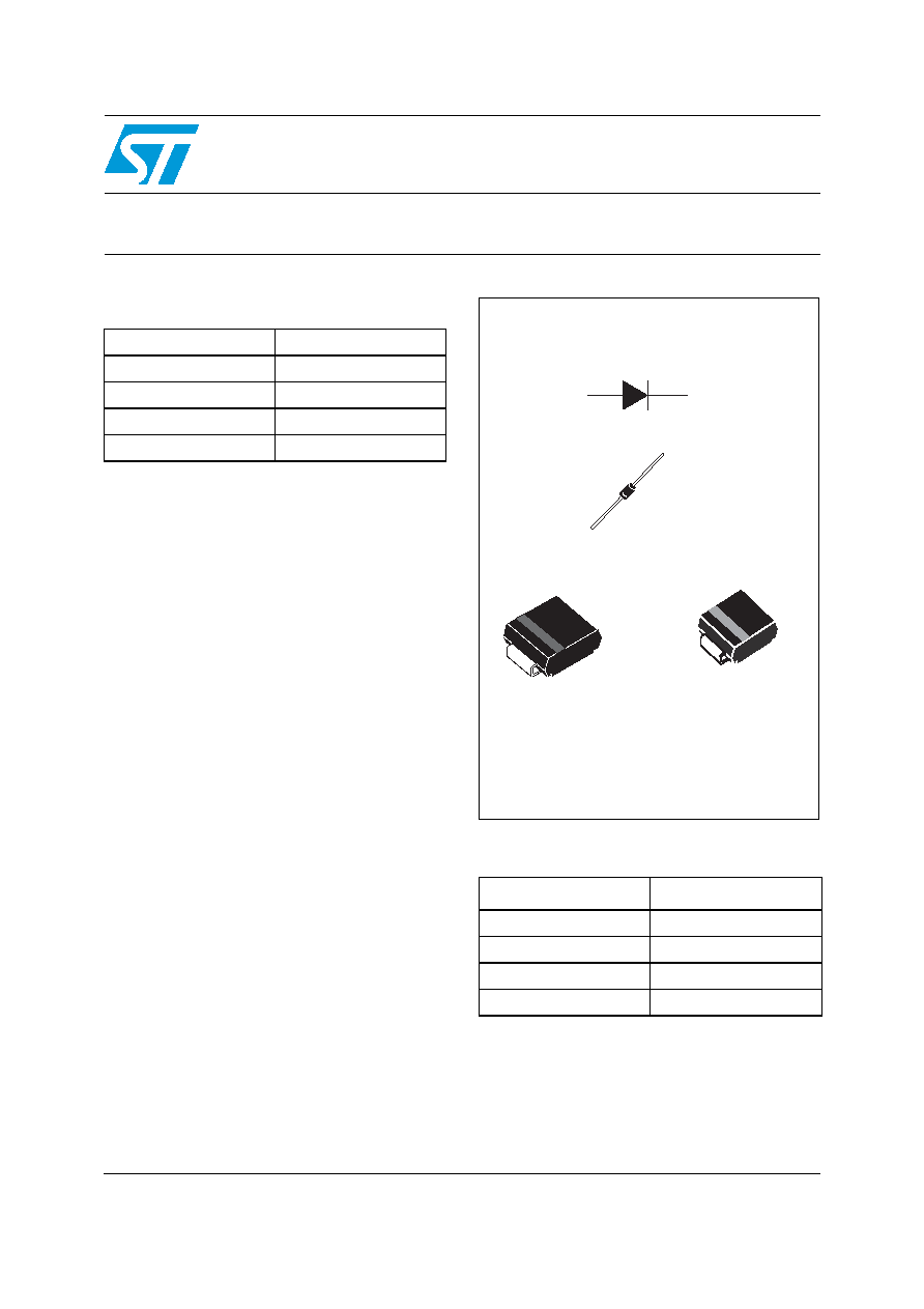
STTH2R02
Ultrafast recovery diode
Main product characteristics
Features and benefits
Very low conduction losses
Negligible switching losses
Low forward and reverse recovery times
High junction temperature
Description
The STTH2R02 uses ST's new 200 V planar Pt
doping technology, and it is specially suited for
switching mode base drive and transistor circuits.
Packaged in DO-15, SMA, and SMB, this device
is intended for use in low voltage, high frequency
inverters, free wheeling and polarity protection.
Order codes
I
F(AV)
2 A
V
RRM
200 V
T
j
(max)
175° C
V
F
(typ)
0.7 V
t
rr
(typ)
15 ns
Part Number
Marking
STTH2R02Q
STTH2R02
STTH2R02QRL
STTH2R02
STTH2R02A
R2A
STTH2R02U
R2U
K
A
K
A
DO-15
STTH2R02Q
SMA
STTH2R02A
SMB
STTH2R02U
K
K
A
A
www.st.com
Characteristics
STTH2R02
2/9
1 Characteristics
To evaluate the conduction losses use the following equation:
P = 0.68 x I
F(AV)
+ 0.06 I
F
2
(RMS)
Table 1.
Absolute ratings (limiting values at T
j
= 25° C, unless otherwise specified)
Symbol
Parameter
Value
Unit
V
RRM
Repetitive peak reverse voltage
200
V
I
FRM
Repetitive peak forward current
DO-15
(1)
t
p
= 5 µs, F = 5 kHz
60
A
SMA, SMB
I
F(RMS)
RMS forward current
DO-15
60
A
SMA, SMB
I
F(AV)
Average forward current,
= 0.5
DO-15
T
lead
= 90° C
2
A
SMA, SMB T
c
= 90° C
I
FSM
Surge non repetitive forward current
t
p
= 10 ms Sinusoidal
75
A
T
stg
Storage temperature range
-65 to + 175
° C
T
j
Maximum operating junction temperature
175
° C
1.
On infinite heatsink with 10 mm lead length
Table 2.
Thermal parameters
Symbol
Parameter
Value
Unit
R
th(j-c)
Junction to lead
Lead Length = 10 mm on infinite heatsink DO-15
45
° C/W
Junction to case
SMA, SMB
30
Table 3.
Static electrical characteristics
Symbol
Parameter
Test conditions
Min.
Typ
Max.
Unit
I
R
(1)
Reverse leakage current
T
j
= 25° C
V
R
= V
RRM
3
µA
T
j
= 125° C
2
20
V
F
(2)
Forward voltage drop
T
j
= 25° C
I
F
= 6 A
1.20
V
T
j
= 25° C
I
F
= 2 A
0.89
1.0
T
j
= 100° C
0.76
0.85
T
j
= 150° C
0.70
0.80
1.
Pulse test: t
p
= 5 ms,
< 2 %
2.
Pulse test: t
p
= 380 µs,
< 2 %
STTH2R02
Characteristics
3/9
Table 4.
Dynamic characteristics
Symbol
Parameter
Test conditions
Min.
Typ
Max.
Unit
t
rr
Reverse recovery time
I
F
= 1 A, dI
F
/dt = -50 A/µs,
V
R
= 30 V, T
j
= 25° C
23
30
ns
I
F
= 1 A, dI
F
/dt = -100 A/µs,
V
R
= 30 V, T
j
= 25° C
15
20
I
RM
Reverse recovery current
I
F
= 2 A, dI
F
/dt = -200 A/µs,
V
R
= 160 V, T
j
= 125° C
3
4
A
t
fr
Forward recovery time
I
F
= 2 A, dI
F
/dt = 100 A/µs
V
FR
= 1.1 x V
Fmax
, T
j
= 25° C
40
ns
V
FP
Forward recovery voltage
I
F
= 2 A, dI
F
/dt = 100 A/µs,
T
j
= 25° C
2.0
V
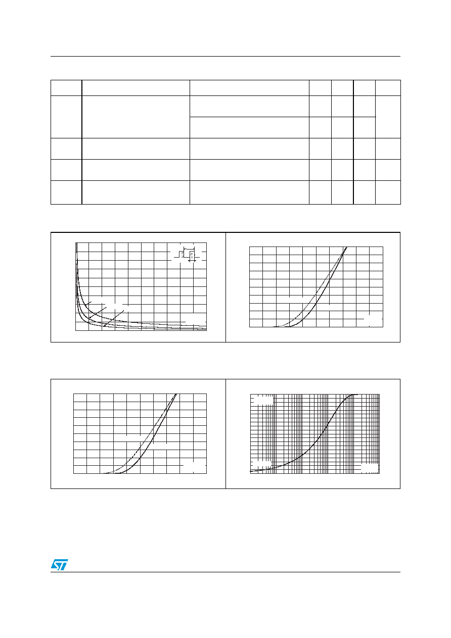
Figure 1.
Peak current versus duty cycle
Figure 2.
Forward voltage drop versus
forward current (typical values)
I
M
(A)
0
20
40
60
80
100
0.0
0.1
0.2
0.3
0.4
0.5
0.6
0.7
0.8
0.9
1.0
T
d=tp/T
tp
I
M
T
=tp/T
tp
I
M
P = 2 W
P = 2 W
P = 1 W
P = 1 W
P = 5 W
P = 5 W
0
10
20
30
40
50
0.0
0.5
1.0
1.5
2.0
2.5
I
FM
(A)
T
j
=25°C
T
j
=150°C
V
FM
(V)
Figure 3.
Forward voltage drop versus
forward current (maximum values)
Figure 4.
Relative variation of thermal
impedance junction to case versus
pulse duration (SMA)
0
10
20
30
40
50
0.0
0.5
1.0
1.5
2.0
2.5
I
FM
(A)
T
j
=25°C
T
j
=150°C
V
FM
(V)
0.0
0.1
0.2
0.3
0.4
0.5
0.6
0.7
0.8
0.9
1.0
1.E-02
1.E-01
1.E+00
1.E+01
1.E+02
1.E+03
Z
th(j-a)
/R
th(j-a)
Single pulse
SMA
S
cu
=1cm²
t
P
(s)
Characteristics
STTH2R02
4/9
Figure 5.
Relative variation of thermal
impedance junction to case versus
pulse duration (SMB)
Figure 6.
Relative variation of thermal
impedance junction to case versus
pulse duration (DO-15)
0.0
0.1
0.2
0.3
0.4
0.5
0.6
0.7
0.8
0.9
1.0
1.E-03
1.E-02
1.E-01
1.E+00
1.E+01
1.E+02
1.E+03
Z
th(j-a)
/R
th(j-a)
Single pulse
SMB
S
cu
=1cm²
t
P
(s)
0.0
0.1
0.2
0.3
0.4
0.5
0.6
0.7
0.8
0.9
1.0
1.E-03
1.E-02
1.E-01
1.E+00
1.E+01
1.E+02
1.E+03
Z
th(j-a)
/R
th(j-a)
Single pulse
DO-15
Lleads=10mm
t
P
(s)
Figure 7.
Junction capacitance versus
reverse applied voltage (typical
values)
Figure 8.
Reverse recovery charges versus
dI
F
/dt (typical values)
1
10
100
1
10
100
1000
C(pF)
F=1MHz
V
osc
=30mV
RMS
T
j
=25°C
V
R
(V)
0
10
20
30
40
50
60
10
100
1000
Q
RR
(nC)
I
F
=2A
V
R
=160V
T
j
=125°C
T
j
=25°C
dI
F
/dt(A/µs)
Figure 9.
Reverse recovery time versus dI
F
/dt
(typical values)
Figure 10.
Peak reverse recovery current
versus dI
F
/dt (typical values)
0
10
20
30
40
50
60
10
100
1000
t
RR
(ns)
I
F
=2A
V
R
=160V
T
j
=125°C
T
j
=25°C
dI
F
/dt(A/µs)
0
1
2
3
4
5
6
10
100
1000
I
RM
(A)
I
F
=2A
V
R
=160V
T
j
=125°C
T
j
=25°C
dI
F
/dt(A/µs)
STTH2R02
Ordering information scheme
5/9
L
2
Ordering information scheme
Figure 11.
Dynamic parameters versus
junction temperature
Figure 12.
Thermal resistance, junction to
ambient, versus copper surface
under each lead - SMA/SMB
(epoxy FR4, e
cu
= 35 µm)
Figure 13.
Thermal resistance, junction to
ambient, versus copper surface
under each lead DO-15
(epoxy FR4, e
cu
= 35 µm)
0.0
0.2
0.4
0.6
0.8
1.0
1.2
1.4
25
50
75
100
125
150
Q
RR
; I
RM
[T
j
] / Q
RR
; I
RM
[T
j
=125°C]
I
RM
Q
RR
I
F
=2A
V
R
=160V
T
j
(°C)
0
20
40
60
80
100
120
0.0
0.5
1.0
1.5
2.0
2.5
3.0
3.5
4.0
4.5
5.0
R
th(j-a)
(°C/W)
SMA
SMB
S
CU
(cm²)
0
10
20
30
40
50
60
70
80
90
100
0.0
0.5
1.0
1.5
2.0
2.5
3.0
3.5
4.0
4.5
5.0
R
th(j-a)
(°C/W)
DO-15
S
CU
(cm²)
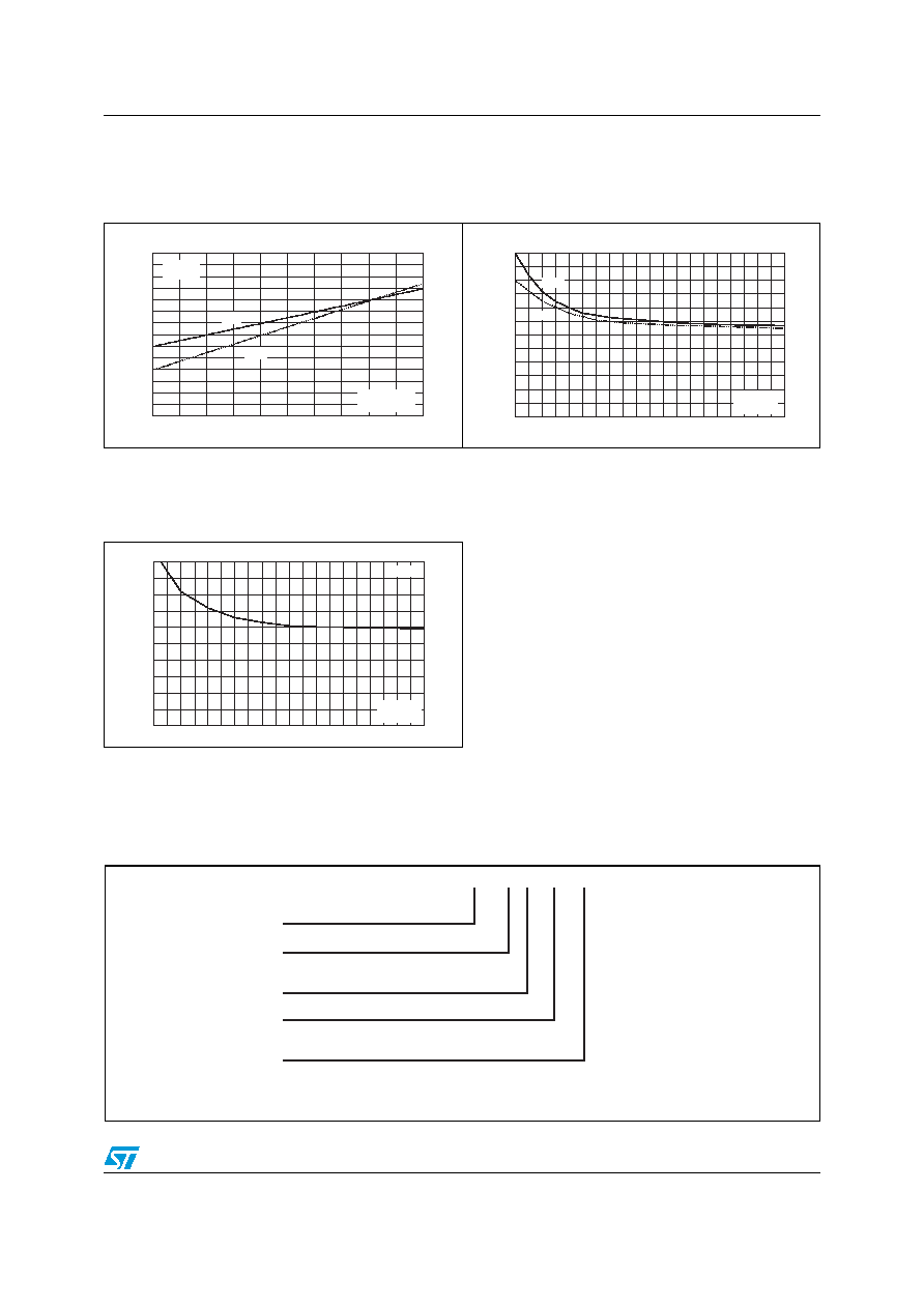
STTH 2 R 02 XXX
Ultrafast switching diode
Average forward current
2 = 2 A
02 = 200 V
Q = DO-15 in Ammopack
QRL = DO-15 in Tape and reel
A = SMA in Tape and reel
U = SMB in Tape and reel
Model R
Package
Repetitive peak reverse voltage
Document Outline