 | –≠–ª–µ–∫—Ç—Ä–æ–Ω–Ω—ã–π –∫–æ–º–ø–æ–Ω–µ–Ω—Ç: STTH2R06U | –°–∫–∞—á–∞—Ç—å:  PDF PDF  ZIP ZIP |
Æ
1/9
Table 1: Main Product Characteristics
I
F(AV)
2 A
V
RRM
600 V
T
j
175∞C
V
F
(typ)
1 V
t
rr
(typ)
35 ns
STTH2R06
HIGH EFFICIENCY ULTRAFAST DIODE
Table 3: Absolute Ratings (limiting values)
Symbol
Parameter
Value
Unit
V
RRM
Repetitive peak reverse voltage
600
V
I
F(RMS)
RMS forward voltage
7
A
I
F(AV)
Average forward current
= 0.5
DO-41
T
L
= 70∞C
2
A
SMA
T
L
= 85∞C
SMB
T
L
= 100∞C
SMC
T
L
= 115∞C
I
FSM
Surge non repetitive forward current
DO-41
t
p
= 10ms
sinusoidal
40
A
SMA / SMB / SMC
30
T
stg
Storage temperature range
-65 to + 175
∞C
T
j
Operating junction temperature range
-40 to + 175
∞C
SMA
STTH2R06A
SMC
STTH2R06S
DO-41
STTH2R06
K
A
SMB
STTH2R06U
June 2005
REV. 2
FEATURES AND BENEFITS
Very low conduction losses
Negligible switching losses
Low forward and reverse recovery times
High junction temperature
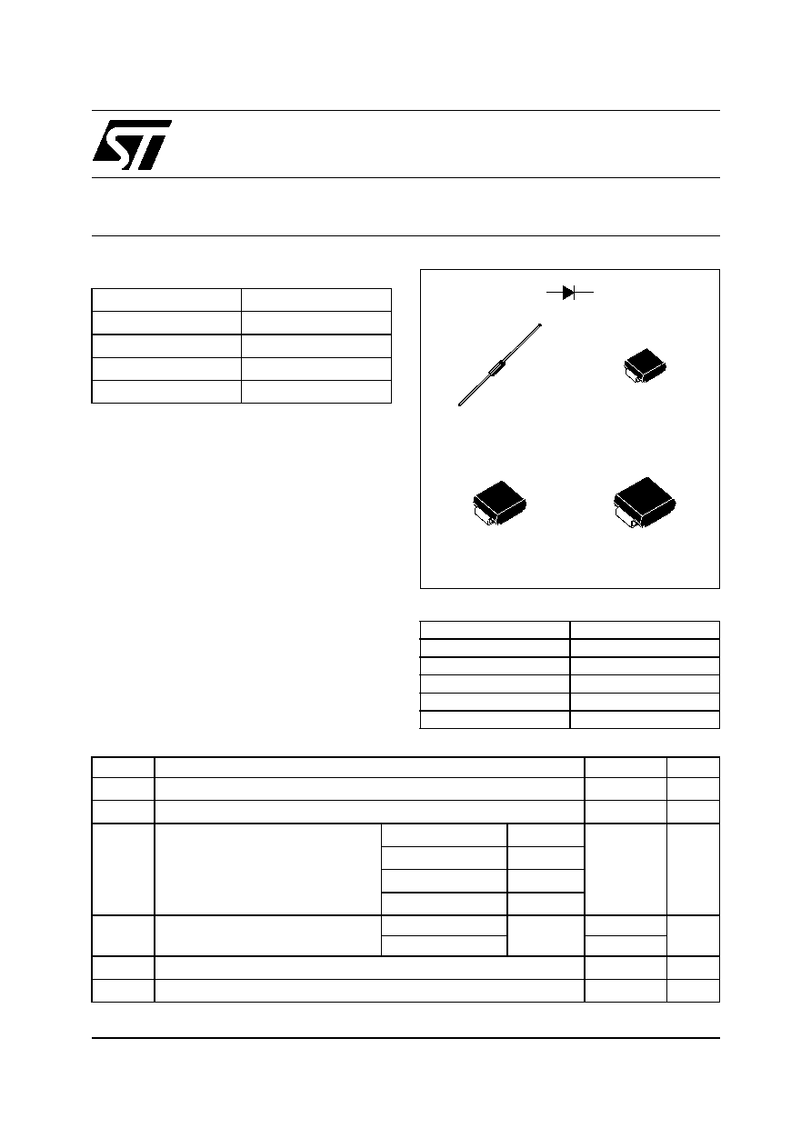
DESCRIPTION
The STTH2R06 is using ST Turbo 2 600V planar
Pt doping technology. It is specially suited for
switching mode base drive & transistor circuits.
Packaged in axial, SMA, SMB and SMC, this de-
vice is intended for use in high frequency inverters,
free wheeling and polarity protection.
Table 2: Order Codes
Part Number
Marking
STTH2R06
STTH2R06
STTH2R06RL
STTH2R06
STTH2R06A
R6A
STTH2R06U
R6U
STTH2R06S
R62
STTH2R06
2/9
Table 4: Thermal Resistance
Table 5: Static Electrical Characteristics
Pulse test:
* tp = 5 ms,
< 2%
** tp = 380 µs,
< 2%
To evaluate the conduction losses use the following equation: P = 1 x IF(AV) + 0.125 IF
2
(RMS)
Table 6: Dynamic Characteristics
Symbol
Parameter
Value (max).
Unit
R
th(j-l)
Junction to lead
DO-41 L = 5 mm
35
∞C/W
SMA
30
SMB
25
SMC
20
Symbol
Parameter
Test conditions
Min.
Typ
Max.
Unit
I
R
*
Reverse leakage current
T
j
= 25∞C
V
R
= V
RRM
2
µA
T
j
= 150∞C
12
85
V
F
**
Forward voltage drop
T
j
= 25∞C
I
F
= 2A
1.7
V
T
j
= 150∞C
1.0
1.25
Symbol
Parameter
Test conditions
Min.
Typ Max.
Unit
t
rr
Reverse recovery
time
T
j
= 25∞C
I
F
= 0.5A Irr = 0.25A I
R
=1A
30
ns
I
F
= 1A dI
F
/dt = -50 A/µs V
R
=30V
35
50
t
fr
Forward recovery
time
T
j
= 25∞C
I
F
= 2A dI
F
/dt = 100 A/µs
V
FR
= 1.1 x V
Fmax
100
ns
V
FP
Forward recovery
voltage
10
V
STTH2R06
3/9
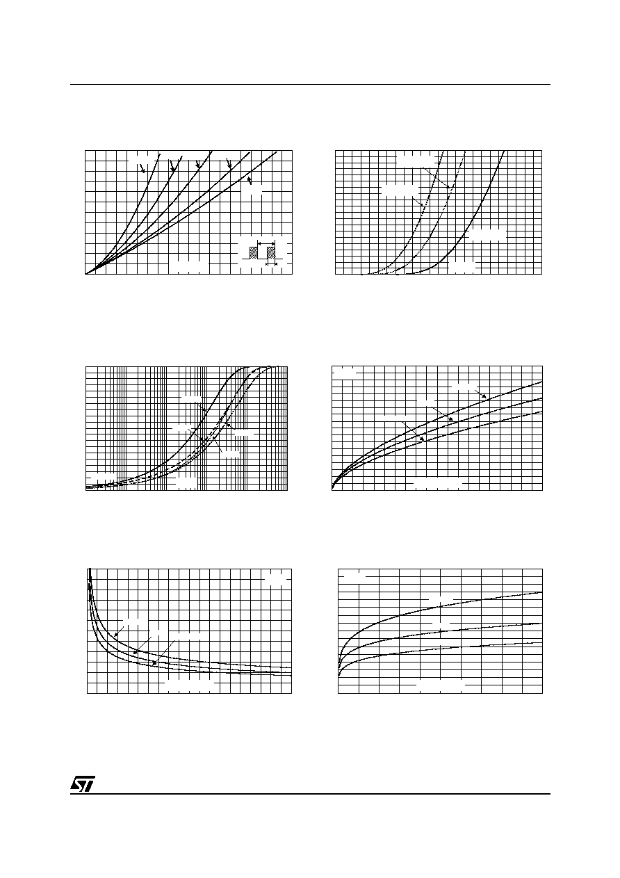
Figure 1: Conduction losses versus average
forward current
Figure 2: Forward voltage drop versus forward
current
Figure 3: Relative variation of thermal
impedance junction to case versus pulse
duration (SMA/SMB/SMC: S
CU
= 1cm
2
)
Figure 4: Peak reverse recovery current
versus dI
F
/dt (typical values)
Figure 5: Reverse recovery time versus dI
F
/dt
(typical values)
Figure 6: Reverse recovery charges versus
dI
F
/dt (typical values)
0.0
0.5
1.0
1.5
2.0
2.5
3.0
0.0
0.5
1.0
1.5
2.0
2.5
P(W)
I
(A)
F(AV)
T
=tp/T
tp
= 0.05
= 0.1
= 0.2
= 1
= 0.5
0
1
2
3
4
5
6
7
8
9
10
0.00
0.25
0.50
0.75
1.00
1.25
1.50
1.75
2.00
2.25
2.50
2.75
3.00
I
(A)
FM
V
(V)
FM
T =150∞C
(typical values)
j
T =25∞C
(maximum values)
j
T =150∞C
(maximum values)
j
0.0
0.1
0.2
0.3
0.4
0.5
0.6
0.7
0.8
0.9
1.0
1.E-02
1.E-01
1.E+00
1.E+01
1.E+02
1.E+03
Z
/R
th(j-a)
th(j-a)
Single pulse
t (s)
p
SMA
DO-41
SMC
SMB
0
1
2
3
4
5
6
7
8
9
0
50
100
150
200
250
300
350
400
450
500
I
(A)
RM
dI /dt(A/µs)
F
I =2 x I
F
F(AV)
I =I
F
F(AV)
I =0.5 x I
F
F(AV)
V =400V
T =125∞C
R
j
0
50
100
150
200
250
300
0
50
100
150
200
250
300
350
400
450
500
t (ns)
rr
dI /dt(A/µs)
F
I =2 x I
F
F(AV)
I =I
F
F(AV)
I =0.5 x I
F
F(AV)
V =400V
T =125∞C
R
j
0
50
100
150
200
250
300
350
400
0
100
200
300
400
500
Q (nC)
rr
I =2 x I
F
F(AV)
I =0.5 x I
F
F(AV)
dI /dt(A/µs)
F
I =I
F
F(AV)
V =400V
T =125∞C
R
j
STTH2R06
4/9
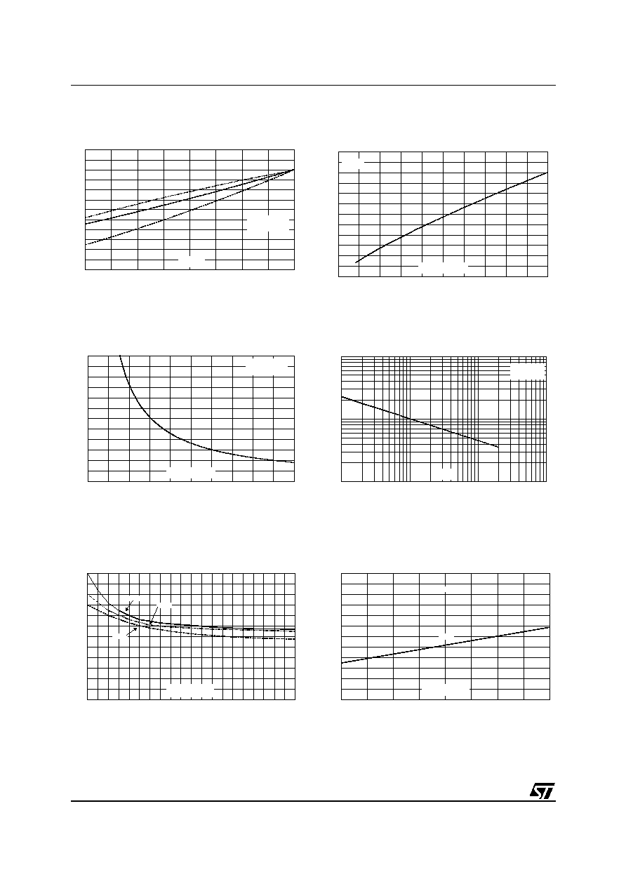
Figure 7: Relative variations of dynamic
parameters versus junction temperature
Figure 8: Transient peak forward voltage
versus dI
F
/dt (typical values)
Figure 9: Forward recovery time versus dI
F
/dt
(typical values)
Figure 10: Junction capacitance versus
reverse voltage applied (typical values)
Figure 11: Thermal resistance junction to
ambient versus copper surface under each
lead (epoxy FR4, e
CU
=35µm) (SMA/SMB/SMC)
Figure 12: Thermal resistance versus lead
length (DO-41)
0.0
0.2
0.4
0.6
0.8
1.0
1.2
25
50
75
100
125
I
RM
Q
RR
t
rr
T (∞C)
j
I =I
Reference: T =125∞C
F
F(AV)
j
V =400V
R
0
5
10
15
20
25
30
0
50
100
150
200
250
V
(V)
FP
dI /dt(A/µs)
F
I =I
T =125∞C
F
F(AV)
j
0
50
100
150
200
250
300
0
50
100
150
200
250
t (ns)
fr
dI /dt(A/µs)
F
I =I
T =125∞C
F
F(AV)
j
V
=1.1 x V max.
FR
F
1
10
100
1
10
100
1000
C(pF)
V (V)
R
F=1MHz
V
=30mV
T =25∞C
OSC
RMS
j
R
(∞C/W)
th(j-a)
0
20
40
60
80
100
120
0.0
0.5
1.0
1.5
2.0
2.5
3.0
3.5
4.0
4.5
5.0
SMA
SMB
SMB
S
(cm≤)
CU
0
20
40
60
80
100
120
5
10
15
20
25
R (∞C/W)
th
L
(mm)
lead
R
th(j-a)
R
th(j-l)
STTH2R06
5/9
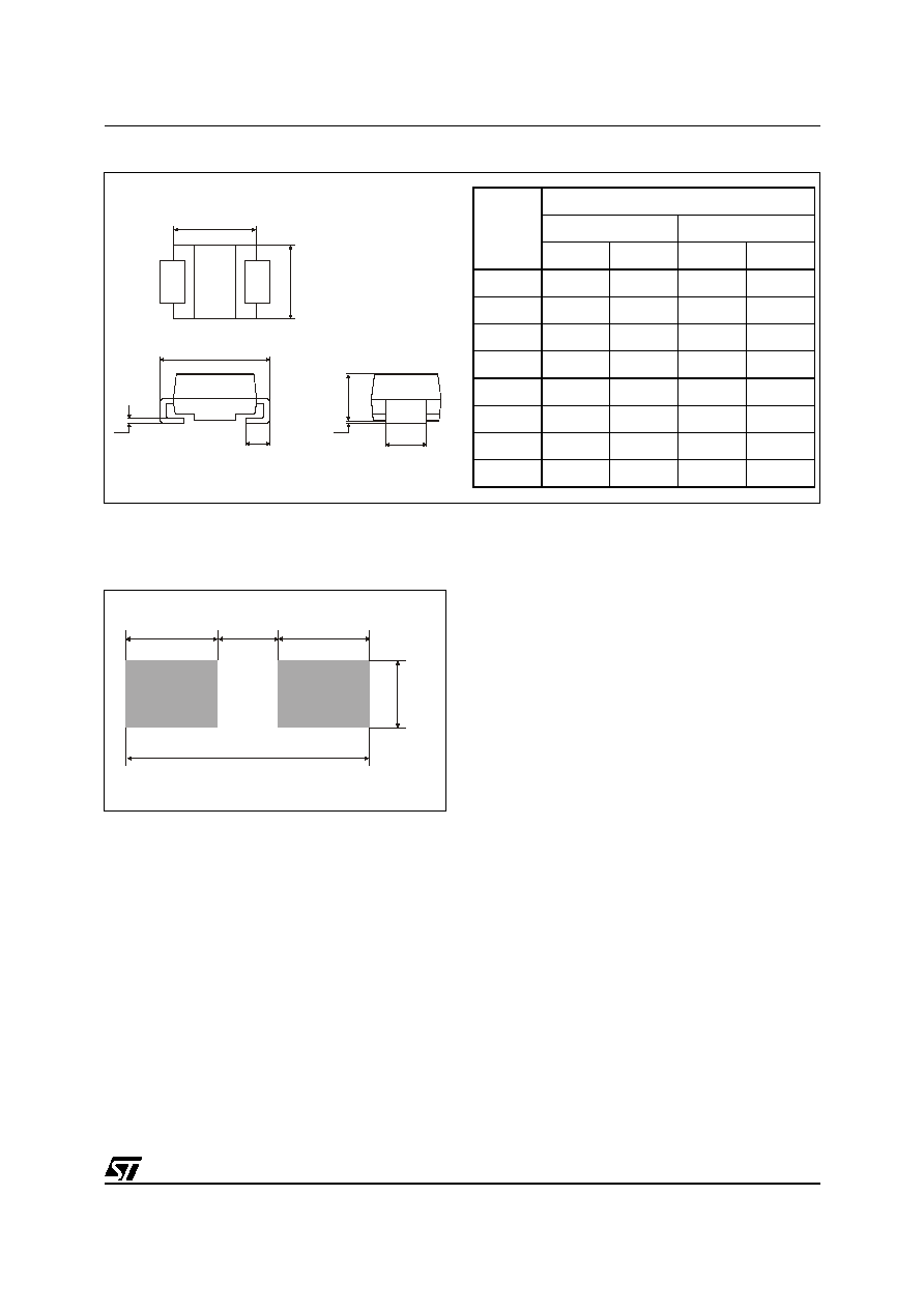
Figure 13: SMA Package Mechanical Data
Figure 14: SMA Foot Print Dimensions
(in millimeters)
E
C
L
E1
D
A1
A2
b
1.50
6.10
2.30
1.75
2.30
REF.
DIMENSIONS
Millimeters
Inches
Min.
Max.
Min.
Max.
A1
1.90
2.03
0.075
0.080
A2
0.05
0.20
0.002
0.008
b
1.25
1.65
0.049
0.065
c
0.15
0.41
0.006
0.016
E
4.80
5.60
0.189
0.220
E1
3.95
4.60
0.156
0.181
D
2.25
2.95
0.089
0.116
L
0.75
1.60
0.030
0.063