 | –≠–ª–µ–∫—Ç—Ä–æ–Ω–Ω—ã–π –∫–æ–º–ø–æ–Ω–µ–Ω—Ç: STTH30L06 | –°–∫–∞—á–∞—Ç—å:  PDF PDF  ZIP ZIP |
Æ
1/9
Table 1: Main Product Characteristics
I
F(AV)
30 A
V
RRM
600 V
T
j
175∞C
V
F
(typ)
1.0 V
t
rr
(max)
65 ns
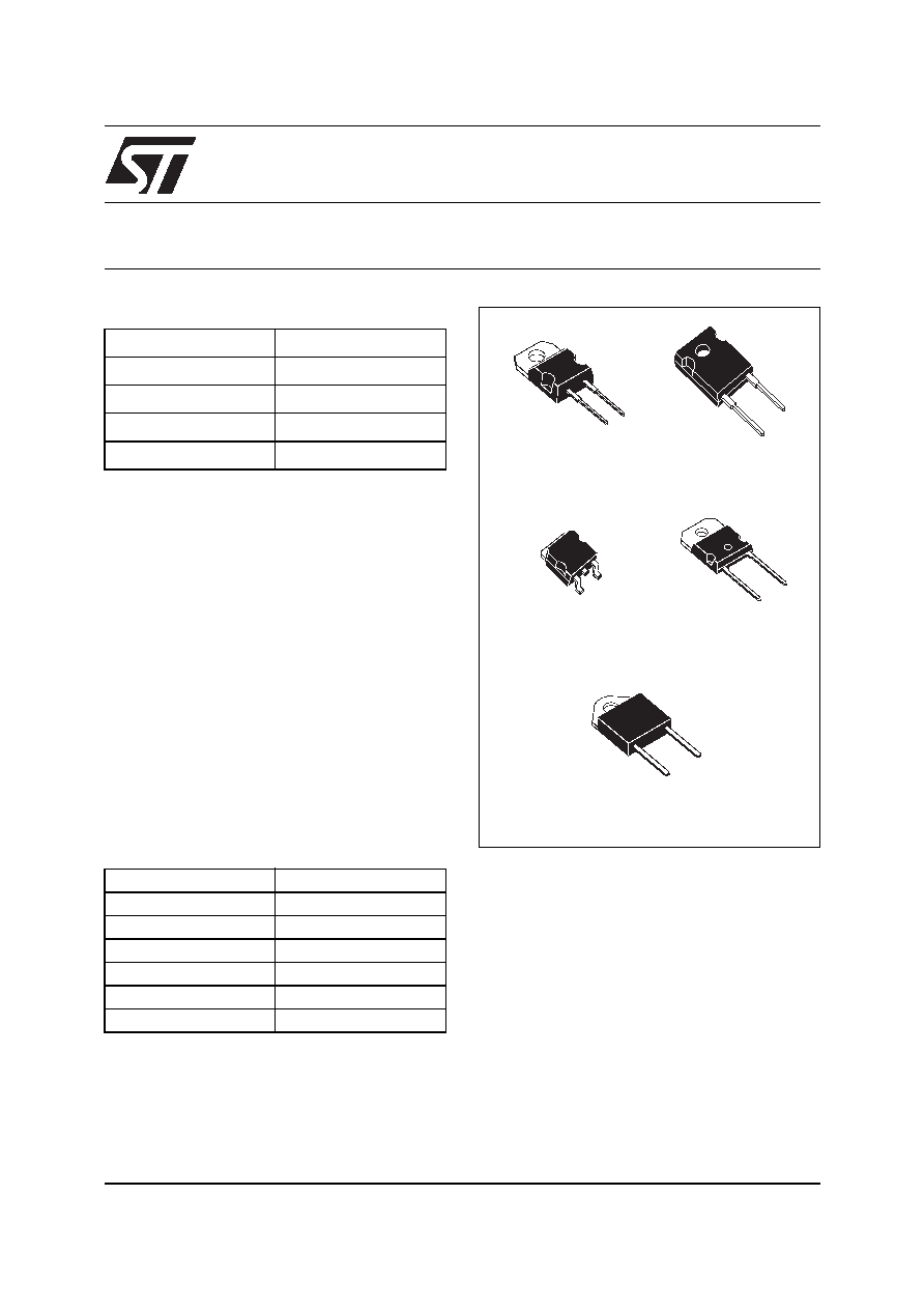
STTH30L06
TURBO 2 ULTRAFAST HIGH VOLTAGE RECTIFIER
K
A
TO-220AC
STTH30L06D
K
A
DO-247
STTH30L06W
K
A
A
D
2
PAK
STTH30L06G
K
A
SOD-93
STTH30L06P
K
A
DOP3I
STTH30L06PI
January 2006
REV. 3
FEATURES AND BENEFITS
Ultrafast switching
Low reverse current
Low thermal resistance
Reduces switching & conduction losses
DESCRIPTION
The STTH30L06, which is using ST Turbo 2 600V
technology, is specially suited for use in switching
power supplies, and industrial applications, as
rectification and discontinuous mode PFC boost
diode.
Table 2: Order Codes
Part Number
Marking
STTH30L06D
STTH30L06D
STTH30L06G
STTH30L06G
STTH30L06G-TR
STTH30L06G
STTH30L06W
STTH30L06W
STTH30L06P
STTH30L06P
STTH30L06PI
STTH30L06PI
STTH30L06
2/9
Table 3: Absolute Ratings (limiting values)
Table 4: Thermal Resistance
Table 5: Static Electrical Characteristics
Pulse test:
* tp = 5 ms,
< 2%
** tp = 380 µs,
< 2%
To evaluate the conduction losses use the following equation: P = 0.95 x IF(AV) + 0.010 IF
2
(RMS)
Table 6: Dynamic Characteristics
Symbol
Parameter
Value
Unit
V
RRM
Repetitive peak reverse voltage
600
V
I
F(RMS)
RMS forward voltage
50
A
I
F(AV)
Average forward current
TO-220AC / TO-247
/ D
2
PAK / SOT-93
Tc = 125∞C
= 0.5
30
A
DOP3I
Tc = 95∞C
= 0.5
I
FSM
Surge non repetitive forward current
tp = 10ms sinusoidal
160
A
T
stg
Storage temperature range
-65 to + 175
∞C
T
j
Maximum operating junction temperature
175
∞C
Symbol
Parameter
Value (max).
Unit
R
th(j-c)
Junction to case
TO-220AC / TO-247 / D
2
PAK / SOT-93
1.1
∞C/W
DOP3I
1.7
Symbol
Parameter
Test conditions
Min.
Typ
Max.
Unit
I
R
*
Reverse leakage current T
j
= 25∞C
V
R
= V
RRM
25
µA
T
j
= 150∞C
80
800
V
F
**
Forward voltage drop
T
j
= 25∞C
I
F
= 30A
1.55
V
T
j
= 150∞C
1.0
1.25
Symbol
Parameter
Test conditions
Min.
Typ Max.
Unit
t
rr
Reverse recovery
time
T
j
= 25∞C
I
F
= 0.5A Irr = 0.25A I
R
=1A
65
ns
I
F
= 1A dI
F
/dt = 50 A/µs V
R
=30V
65
90
I
RM
Reverse recovery
current
T
j
= 125∞C I
F
= 30A V
R
= 400V
dI
F
/dt = 100 A/µs
11.5
16
A
t
fr
Forward recovery
time
T
j
= 25∞C
I
F
= 30A dI
F
/dt = 100 A/µs
V
FR
= 1.1 x V
Fmax
500
ns
V
FP
Forward recovery
voltage
T
j
= 25∞C
I
F
= 30A dI
F
/dt = 100 A/µs
V
FR
= 1.1 x V
Fmax
2.5
V

STTH30L06
3/9
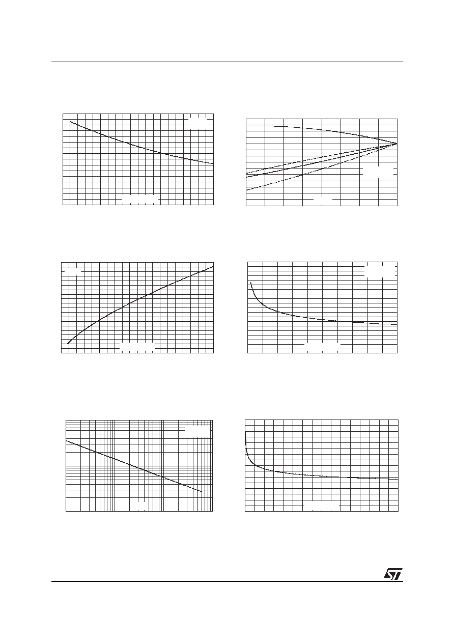
Figure 1: Conduction losses versus average
forward current
Figure 2: Forward voltage drop versus forward
current
Figure 3: Relative variation of thermal
impedance junction to case versus pulse
duration
Figure 4: Peak reverse recovery current
versus dI
F
/dt (typical values)
Figure 5: Reverse recovery time versus dI
F
/dt
(typical values)
Figure 6: Reverse recovery charges versus
dI
F
/dt (typical values)
P(W)
0
5
10
15
20
25
30
35
40
45
50
0
5
10
15
20
25
30
35
40
T
=tp/T
tp
I
(A)
F(AV)
= 1
= 0.05
= 0.1
= 0.2
= 0.5
0
10
20
30
40
50
60
70
80
90
100
0.00
0.25
0.50
0.75
1.00
1.25
1.50
1.75
2.00
2.25
2.50
I
(A)
FM
V
(V)
FM
T =150∞C
(typical values)
j
T =25∞C
(maximum values)
j
T =150∞C
(maximum values)
j
0.0
0.1
0.2
0.3
0.4
0.5
0.6
0.7
0.8
0.9
1.0
1.E-03
1.E-02
1.E-01
1.E+00
Z
/R
th(j-c)
th(j-c)
t (s)
p
Single pulse
0
5
10
15
20
25
30
35
40
45
0
50
100
150
200
250
300
350
400
450
500
I
(A)
RM
dI /dt(A/µs)
F
I =2 x I
F
F(AV)
I =I
F
F(AV)
I =0.5 x I
F
F(AV)
V =400V
T =125∞C
R
j
0
50
100
150
200
250
300
350
400
450
500
550
600
650
700
750
800
0
50
100
150
200
250
300
350
400
450
500
t (ns)
rr
dI /dt(A/µs)
F
I =I
F
F(AV)
I =0.5 x I
F
F(AV)
V =400V
T =125∞C
R
j
I =2 x I
F
F(AV)
0
500
1000
1500
2000
2500
3000
3500
0
100
200
300
400
500
Q (nC)
rr
I =2 x I
F
F(AV)
I =I
F
F(AV)
I =0.5 x I
F
F(AV)
V =400V
T =125∞C
R
j
dI /dt(A/µs)
F
STTH30L06
4/9
Figure 7: Reverse recovery softness factor
versus dI
F
/dt (typical values)
Figure 8: Relative variations of dynamic
parameters versus junction temperature
Figure 9: Transient peak forward voltage
versus dI
F
/dt (typical values)
Figure 10: Forward recovery time versus dI
F
/dt
(typical values)
Figure 11: Junction capacitance versus
reverse voltage applied (typical values)
Figure 12: Thermal resistance junction to
ambient versus copper surface under tab
(epoxy FR4, e
CU
=35µm) (D
2
PAK)
0.0
0.2
0.4
0.6
0.8
1.0
1.2
1.4
1.6
0
50
100
150
200
250
300
350
400
450
500
S factor
I < 2 x I
T =125∞C
F
F(AV)
j
V =400V
R
dI /dt(A/µs)
F
0.0
0.2
0.4
0.6
0.8
1.0
1.2
1.4
25
50
75
100
125
I
RM
Q
RR
t
rr
S factor
T (∞C)
j
I =I
Reference: T =125∞C
F
F(AV)
j
V =400V
R
0
1
2
3
4
5
6
7
8
9
10
0
50
100
150
200
250
300
350
400
450
500
V
(V)
FP
dI /dt(A/µs)
F
I =I
T =125∞C
F
F(AV)
j
0
50
100
150
200
250
300
350
400
450
500
0
100
200
300
400
500
t (ns)
fr
dI /dt(A/µs)
F
I =I
T =125∞C
F
F(AV)
j
V
=1.1 x V max.
FR
F
10
100
1000
1
10
100
1000
C(pF)
V (V)
R
F=1MHz
V
=30mV
T =25∞C
OSC
RMS
j
R
(∞C/W)
th(j-a)
0
10
20
30
40
50
60
70
80
0
5
10
15
20
25
30
35
40
S
(cm≤)
CU
STTH30L06
5/9
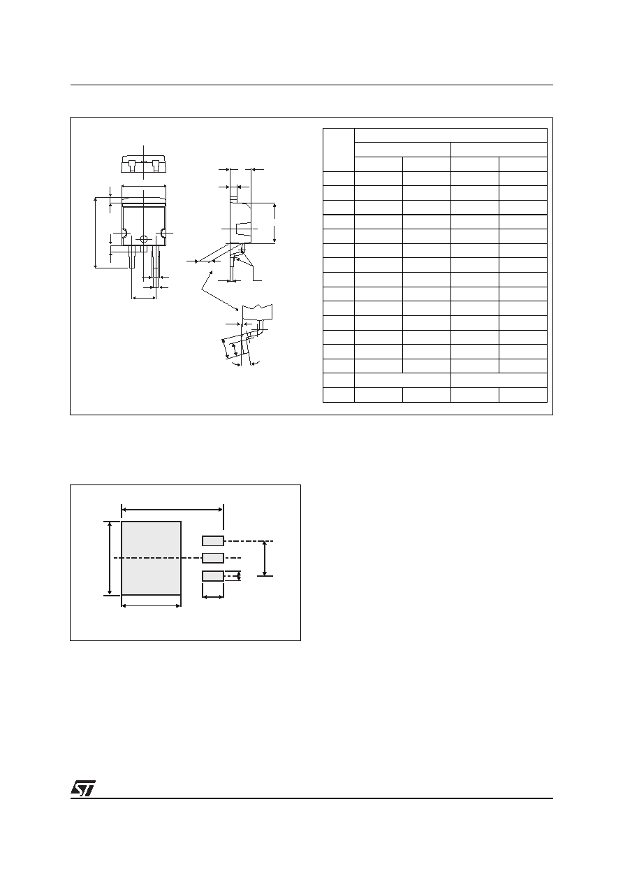
Figure 13: D
2
PAK Package Mechanical Data
Figure 14: D
2
PAK Foot Print Dimensions
(in millimeters)
A
C2
D
R
A2
M
V2
C
A1
G
L
L3
L2
B
B2
E
*
* FLAT ZONE NO LESSTHAN 2mm
REF.
DIMENSIONS
Millimeters
Inches
Min.
Max.
Min.
Max.
A
4.40
4.60
0.173
0.181
A1
2.49
2.69
0.098
0.106
A2
0.03
0.23
0.001
0.009
B
0.70
0.93
0.027
0.037
B2
1.14
1.70
0.045
0.067
C
0.45
0.60
0.017
0.024
C2
1.23
1.36
0.048
0.054
D
8.95
9.35
0.352
0.368
E
10.00
10.40
0.393
0.409
G
4.88
5.28
0.192
0.208
L
15.00
15.85
0.590
0.624
L2
1.27
1.40
0.050
0.055
L3
1.40
1.75
0.055
0.069
M
2.40
3.20
0.094
0.126
R
0.40 typ.
0.016 typ.
V2
0∞
8∞
0∞
8∞
8.90
3.70
1.30
5.08
16.90
10.30