
Æ
1/8
Table 1: Main Product Characteristics
I
F(AV)
30 A
V
RRM
600 V
T
j
175∞C
V
F
(typ)
1.10 V
t
rr
(max)
50 ns
STTH30R06
TURBO 2 ULTRAFAST HIGH VOLTAGE RECTIFIER
Table 3: Absolute Ratings (limiting values)
Symbol
Parameter
Value
Unit
V
RRM
Repetitive peak reverse voltage
600
V
I
F(RMS)
RMS forward voltage
50
A
I
F(AV)
Average forward current
TO-220AC / DO-247
/ SOD-93
Tc = 115∞C
= 0.5
30
A
DOP3I
Tc = 85∞C
= 0.5
I
FSM
Surge non repetitive forward current
tp = 10ms sinusoidal
160
A
T
stg
Storage temperature range
-65 to + 175
∞C
T
j
Maximum operating junction temperature
175
∞C
K
A
TO-220AC
STTH30R06D
K
A
DO-247
STTH30R06W
K
A
SOD-93
STTH30R06P
K
A
DOP3I
STTH30R06PI
October 2004
REV. 0C
FEATURES AND BENEFITS
Ultrafast switching
Low reverse current
Low thermal resistance
Reduces switching & conduction losses
DESCRIPTION
The STTH30R06, which is using ST Turbo 2 600V
technology, is specially suited for use in switching
power supplies, and industrial applications, as
rectification and discontinuous mode PFC boost
diode.
Table 2: Order Codes
Part Number
Marking
STTH30R06D
STTH30R06D
STTH30R06W
STTH30R06W
STTH30R06P
STTH30R06P
STTH30R06PI
STTH30R06PI
STTH30R06
2/8
Table 4: Thermal Resistance
Table 5: Static Electrical Characteristics
Pulse test:
* tp = 5 ms,
< 2%
** tp = 380 µs,
< 2%
To evaluate the conduction losses use the following equation: P = 1.07 x IF(AV) + 0.011 IF
2
(RMS)
Table 6: Dynamic Characteristics
Symbol
Parameter
Value (max).
Unit
R
th(j-c)
Junction to case
TO-220AC / DO-247/ SOD-93
1.1
∞C/W
DOP3I
1.7
Symbol
Parameter
Test conditions
Min.
Typ
Max.
Unit
I
R
*
Reverse leakage current T
j
= 25∞C
V
R
= V
RRM
25
µA
T
j
= 150∞C
80
800
V
F
**
Forward voltage drop
T
j
= 25∞C
I
F
= 30A
1.85
V
T
j
= 150∞C
1.10
1.40
Symbol
Parameter
Test conditions
Min.
Typ Max.
Unit
t
rr
Reverse recovery
time
T
j
= 25∞C
I
F
= 0.5A Irr = 0.25A I
R
=1A
50
ns
I
F
= 1A dI
F
/dt = 50 A/µs V
R
=30V
50
70
I
RM
Reverse recovery
current
T
j
= 125∞C I
F
= 30A V
R
= 400V
dI
F
/dt = 100 A/µs
8
11
A
t
fr
Forward recovery
time
T
j
= 25∞C
I
F
= 30A dI
F
/dt = 100 A/µs
V
FR
= 1.1 x V
Fmax
500
ns
V
FP
Forward recovery
voltage
T
j
= 25∞C
I
F
= 30A dI
F
/dt = 100 A/µs
V
FR
= 1.1 x V
Fmax
2.5
V
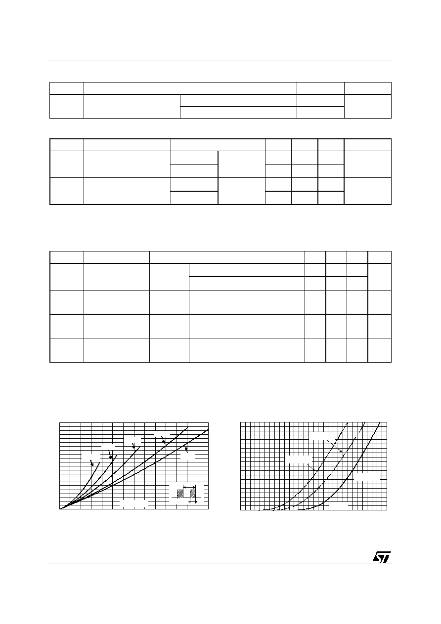
Figure 1: Conduction losses versus average
forward current
Figure 2: Forward voltage drop versus forward
current
0
5
10
15
20
25
30
35
40
45
50
55
0
5
10
15
20
25
30
35
P(W)
T
=tp/T
tp
I
(A)
F(AV)
= 1
= 0.05
= 0.1
= 0.2
= 0.5
0
20
40
60
80
100
120
140
160
180
200
0.0
0.2
0.4
0.6
0.8
1.0
1.2
1.4
1.6
1.8
2.0
2.2
2.4
2.6
2.8
3.0
I
(A)
FM
V
(V)
FM
T =150∞C
(typical values)
j
T =25∞C
(maximum values)
j
T =150∞C
(maximum values)
j
STTH30R06
3/8
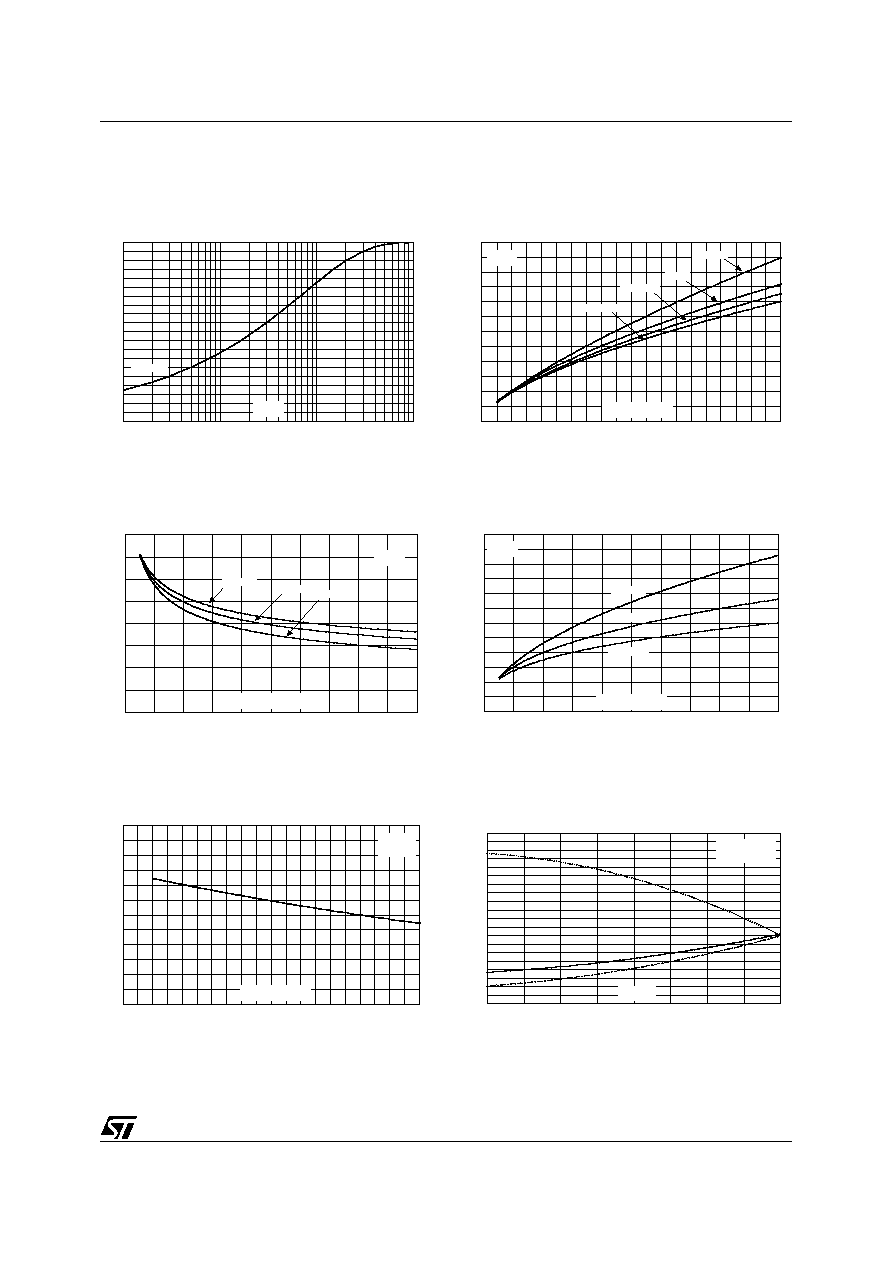
Figure 3: Relative variation of thermal
impedance junction to case versus pulse
duration
Figure 4: Peak reverse recovery current versus
dI
F
/dt (typical values)
Figure 5: Reverse recovery time versus dI
F
/dt
(typical values)
Figure 6: Reverse recovery charges versus
dI
F
/dt (typical values)
Figure 7: Softness factor versus dI
F
/dt (typical
values)
Figure 8: Relative variations of dynamic
parameters versus junction temperature
0.0
0.1
0.2
0.3
0.4
0.5
0.6
0.7
0.8
0.9
1.0
1.E-03
1.E-02
1.E-01
1.E+00
Z
/R
th(j-c)
th(j-c)
t (s)
p
Single pulse
0
5
10
15
20
25
30
0
50
100
150
200
250
300
350
400
450
500
I
(A)
RM
dI /dt(A/µs)
F
I =2 x I
F
F(AV)
I =I
F
F(AV)
I =0.5 x I
F
F(AV)
I =0.25 x I
F
F(AV)
V =400V
T =125∞C
R
j
0
50
100
150
200
0
200
400
600
800
1000
t (ns)
rr
dI /dt(A/µs)
F
I =I
F
F(AV)
I =0.5 x I
F
F(AV)
V =400V
T =125∞C
R
j
I =2 x I
F
F(AV)
0.0
0.5
1.0
1.5
2.0
2.5
3.0
0
200
400
600
800
1000
Q (µC)
rr
I =2 x I
F
F(AV)
I =I
F
F(AV)
I =0.5 x I
F
F(AV)
V =400V
T =125∞C
R
j
dI /dt(A/µs)
F
0.0
0.1
0.2
0.3
0.4
0.5
0.6
0
50
100
150
200
250
300
350
400
450
500
S factor
I
2 x I
T =125∞C
F
F(AV)
j
V =400V
R
dI /dt(A/µs)
F
0.00
0.25
0.50
0.75
1.00
1.25
1.50
1.75
2.00
2.25
2.50
25
50
75
100
125
I
RM
Q
RR
S factor
T (∞C)
j
I =I
Reference: T =125∞C
F
F(AV)
j
V =400V
R
STTH30R06
4/8
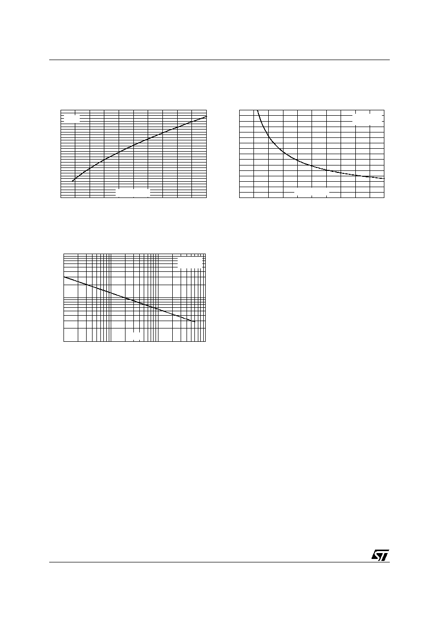
Figure 9: Transient peak forward voltage
versus dI
F
/dt (typical values)
Figure 10: Forward recovery time versus dI
F
/dt
(typical values)
Figure 11: Junction capacitance versus
reverse voltage applied (typical values)
0.0
0.5
1.0
1.5
2.0
2.5
3.0
3.5
4.0
4.5
5.0
5.5
6.0
6.5
7.0
7.5
8.0
0
100
200
300
400
500
V
(V)
FP
dI /dt(A/µs)
F
I =I
T =125∞C
F
F(AV)
j
0
100
200
300
400
500
600
700
800
0
100
200
300
400
500
t (ns)
fr
dI /dt(A/µs)
F
I =I
T =125∞C
F
F(AV)
j
V
=1.1 x V max.
FR
F
10
100
1000
1
10
100
1000
C(pF)
V (V)
R
F=1MHz
V
=30mV
T =25∞C
OSC
RMS
j
STTH30R06
5/8
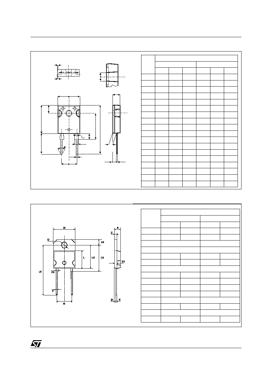
Figure 12: DO-247 Package Mechanical Data
Figure 13: SOD-93 Package Mechanical Data
F2
V2
L4
L2
L1
L3
D
L
L5
M
E
H
V
V
A
Dia.
F3
G
F
REF.
DIMENSIONS
Millimeters
Inches
Min.
Typ. Max. Min.
Typ. Max.
A
4.85
5.15 0.191
0.203
D
2.20
2.60 0.086
0.102
E
0.40
0.80 0.015
0.031
F
1.00
1.40 0.039
0.055
F2
2.00
0.078
F3
2.00
2.40 0.078
0.094
G
10.90
0.429
H
15.45
15.75 0.608
0.620
L
19.85
20.15 0.781
0.793
L1
3.70
4.30 0.145
0.169
L2
18.50
0.728
L3
14.20
14.80 0.559
0.582
L4
34.60
1.362
L5
5.50
0.216
M
2.00
3.00 0.078
0.118
V
5∞
5∞
V2
60∞
60∞
Dia.
3.55
3.65 0.139
0.143
REF.
DIMENSIONS
Millimeters
Inches
Min.
Max.
Min.
Max.
A
4.70
4.90
0.185
0.193
C
1.17
1.37
0.046
0.054
D
2.50 Typ.
0.098 Typ.
D1
1.27 Typ.
0.050 Typ.
E
0.50
0.78
0.020
0.031
F
1.10
1.30
0.043
0.051
F3
1.75 Typ.
0.069 Typ
G
10.80
11.10
0.425
0.437
H
14.70
15.20
0.578
0.598
L
12.20
0.480
L2
16.20
0.638
L3
18.0 Typ
0.709 Typ.
L5
3.95
4.15
0.156
0.163
L6
31.00 Typ.
1.220 Typ.
O
4.00
4.10
0.157
0.161