 | –≠–ª–µ–∫—Ç—Ä–æ–Ω–Ω—ã–π –∫–æ–º–ø–æ–Ω–µ–Ω—Ç: STTH3R06U | –°–∫–∞—á–∞—Ç—å:  PDF PDF  ZIP ZIP |
Æ
1/9
Table 1: Main Product Characteristics
I
F(AV)
3 A
V
RRM
600 V
I
R
(max)
100 µA
T
j
175∞C
V
F
(typ)
1.0 V
t
rr
(typ)
35 ns
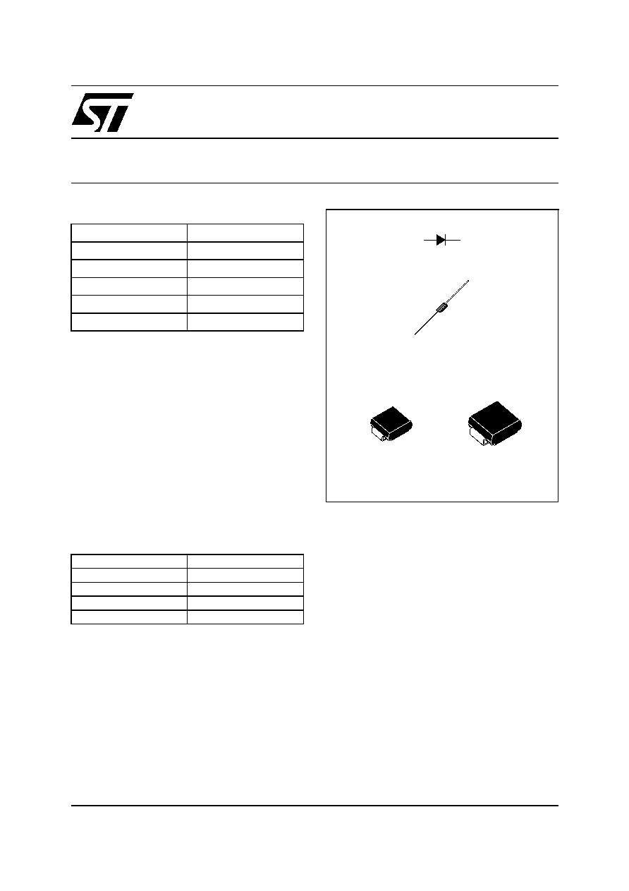
STTH3R06
TURBO 2 ULTRAFAST HIGH VOLTAGE RECTIFIER
SMB
STTH3R06U
SMC
STTH3R06S
DO-201AD
STTH3R06
K
A
September 2004
REV. 2
FEATURES AND BENEFITS
Ultrafast switching
Low forward voltage drop
Low thermal resistance
Low leakage current (platinium doping)
DESCRIPTION
The STTH3R06, which is using ST Turbo 2 600V
technology, is specially suited for use in switching
power supplies, inverters and as a free wheeling
diode.
Table 2: Order Codes
Part Number
Marking
STTH3R06
STTH3R06
STTH3R06RL
STTH3R06
STTH3R06U
R06U
STTH3R06S
R6S
STTH3R06
2/9
Table 3: Absolute Ratings (limiting values)
Table 4: Thermal Parameters
Table 5: Static Electrical Characteristics
To evaluate the conduction losses use the following equation: P = 1.03 x I
F(AV)
+ 0.09 I
F
2
(RMS)
Table 6: Dynamic Characteristics
Symbol
Parameter
Value
Unit
V
RRM
Repetitive peak reverse voltage
600
V
I
F(RMS)
RMS forward voltage
10
A
I
F(AV)
Average forward current
= 0.5
DO-201AD
Tl = 80∞C
3
A
SMB
Tl = 55∞C
SMC
Tl = 80∞C
I
FSM
Surge non repetitive forward current
DO-201AD
tp = 10ms
sinusoidal
55
A
SMB / SMC
45
T
stg
Storage temperature range
-65 to + 175
∞C
T
j
Maximum operating junction temperature
175
∞C
Symbol
Parameter
Maximum
Unit
R
th(j-l)
Junction to lead
DO-201AD L = 10 mm
20
∞C/W
SMB
25
SMC
20
R
th(j-a)
Junction to ambient (see fig. 13)
DO-201AD L = 10 mm
75
∞C/W
Symbol
Parameter
Test conditions
Min.
Typ
Max.
Unit
I
R
Reverse leakage current
T
j
= 25∞C
V
R
= V
RRM
3
µA
T
j
= 150∞C
15
100
V
F
Forward voltage drop
T
j
= 25∞C
I
F
= 3A
1.7
V
T
j
= 150∞C
1.0
1.25
Symbol
Parameter
Test conditions
Min.
Typ Max.
Unit
t
rr
Reverse recovery
time
T
j
= 25∞C
I
F
= 0.5A I
RR
= 0.25A I
R
= 1A
30
ns
I
F
= 1A dI
F
/dt = -50 A/µs V
R
=30V
35
t
fr
Forward recovery
time
T
j
= 25∞C
I
F
= 3A dI
F
/dt = 100 A/µs
V
FR
= 1.1 x V
Fmax
100
ns
V
FP
Forward recovery
voltage
I
F
= 3A dI
F
/dt = 100 A/µs
10
V
STTH3R06
3/9
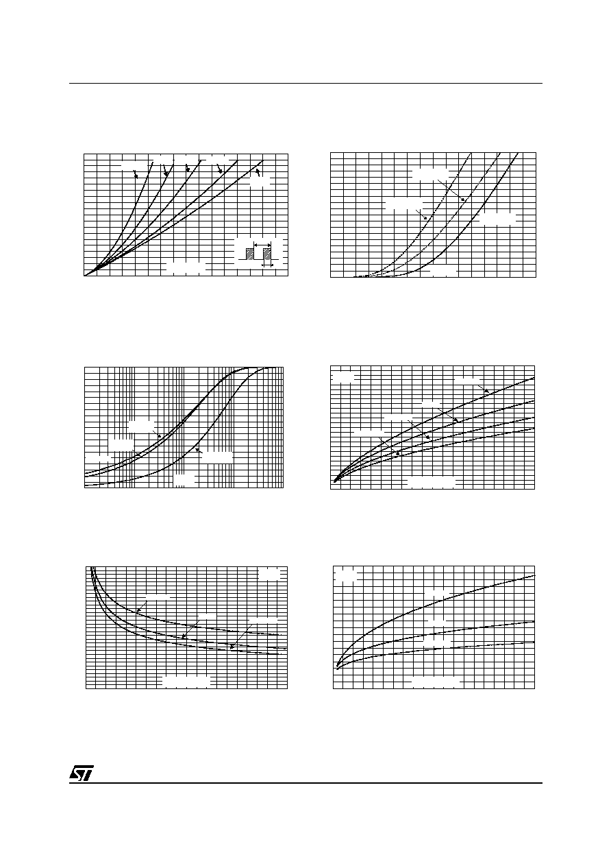
Figure 1: Conduction losses versus average
current
Figure 2: Forward voltage drop versus forward
current
Figure 3: Relative variation of thermal impedance
junction ambient versus pulse duration (epoxy
printed circuit FR4, L
leads
= 10mm, S
CU
=1cm
2
)
Figure 4: Peak reverse recovery current
versus dI
F
/dt (typical values)
Figure 5: Reverse recovery time versus dI
F
/dt
(typical values)
Figure 6: Reverse recovery charges versus
dI
F
/dt (typical values)
0.0
0.5
1.0
1.5
2.0
2.5
3.0
3.5
4.0
4.5
5.0
0.0
0.5
1.0
1.5
2.0
2.5
3.0
3.5
4.0
P(W)
T
=tp/T
tp
= 0.05
= 1
= 0.1
I
(A)
F(AV)
= 0.5
= 0.2
0
5
10
15
20
25
30
35
40
45
50
0.0
0.5
1.0
1.5
2.0
2.5
3.0
3.5
4.0
I
(A)
FM
V
(V)
FM
T =150∞C
(typical values)
j
T =25∞C
(maximum values)
j
T =150∞C
(maximum values)
j
0.0
0.1
0.2
0.3
0.4
0.5
0.6
0.7
0.8
0.9
1.0
1.E-01
1.E+00
1.E+01
1.E+02
1.E+03
Z
/R
th(j-a)
th(j-a)
t (s)
p
DO-201AD
L
= 10mm
leads
SMB
S
= 1cm
Cu
2
SMC
S
= 1cm
Cu
2
Single pulse
0
1
2
3
4
5
6
7
8
9
10
11
12
13
0
50
100
150
200
250
300
350
400
450
500
I
(A)
RM
dI /dt(A/µs)
F
I =2 x I
F
F(AV)
I =I
F
F(AV)
I =0.5 x I
F
F(AV)
I =0.25 x I
F
F(AV)
V =400V
T =125∞C
R
j
0
10
20
30
40
50
60
70
80
90
100
110
120
130
140
150
160
0
50
100
150
200
250
300
350
400
450
500
t (ns)
rr
I =I
F
F(AV)
I =0.5 x I
F
F(AV)
I =2 x I
F
F(AV)
V =400V
T =125∞C
R
j
dI /dt(A/µs)
F
0
50
100
150
200
250
300
350
400
450
0
50
100
150
200
250
300
350
400
450
500
Q (nC)
rr
I =2 x I
F
F(AV)
I =I
F
F(AV)
I =0.5 x I
F
F(AV)
V =400V
T =125∞C
R
j
dI /dt(A/µs)
F
STTH3R06
4/9
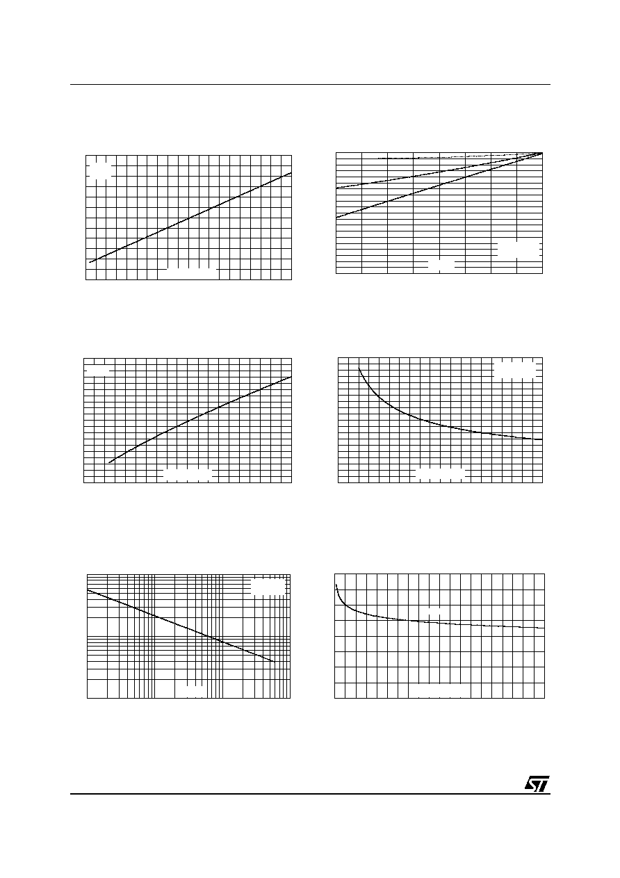
Figure 7: Softness factor versus d
IF
/dt (typical
values)
Figure 8: Relative variations of dynamic
parameters versus junction temperature
Figure 9: Transient peak forward voltage
versus dI
F
/dt (typical values)
Figure 10: Forward recovery time versus dI
F
/dt
(typical values)
Figure 11: Junction capacitance versus
reverse voltage applied (typical values)
Figure 12: Thermal resistance junction to
ambient versus copper surface under lead
(epoxy FR4, e
CU
=35µm) (DO-201AD)
0.0
0.5
1.0
1.5
2.0
2.5
3.0
0
50
100
150
200
250
300
350
400
450
500
S factor
I =I
T =125∞C
F
F(AV)
j
V =400V
R
dI /dt(A/µs)
F
0.0
0.1
0.2
0.3
0.4
0.5
0.6
0.7
0.8
0.9
1.0
25
50
75
100
125
I
RM
Q
RR
S factor
T (∞C)
j
I =I
Reference: T =125∞C
F
F(AV)
j
V =400V
R
0
2
4
6
8
10
12
14
16
18
20
0
20
40
60
80
100
120
140
160
180
200
V
(V)
FP
dI /dt(A/µs)
F
I =I
T =125∞C
F
F(AV)
j
0
20
40
60
80
100
120
140
160
180
200
0
20
40
60
80
100
120
140
160
180
200
t (ns)
fr
I =I
T =125∞C
F
F(AV)
j
V
=1.1 x V max.
FR
F
dI /dt(A/µs)
F
1
10
100
1
10
100
1000
C(pF)
V (V)
R
F=1MHz
V
=30mV
T =25∞C
OSC
RMS
j
0
10
20
30
40
50
60
70
80
0
1
2
3
4
5
6
7
8
9
10
S
(cm≤)
CU
R
(∞C/W)
th(j-a)
DO-201AD
STTH3R06
5/9
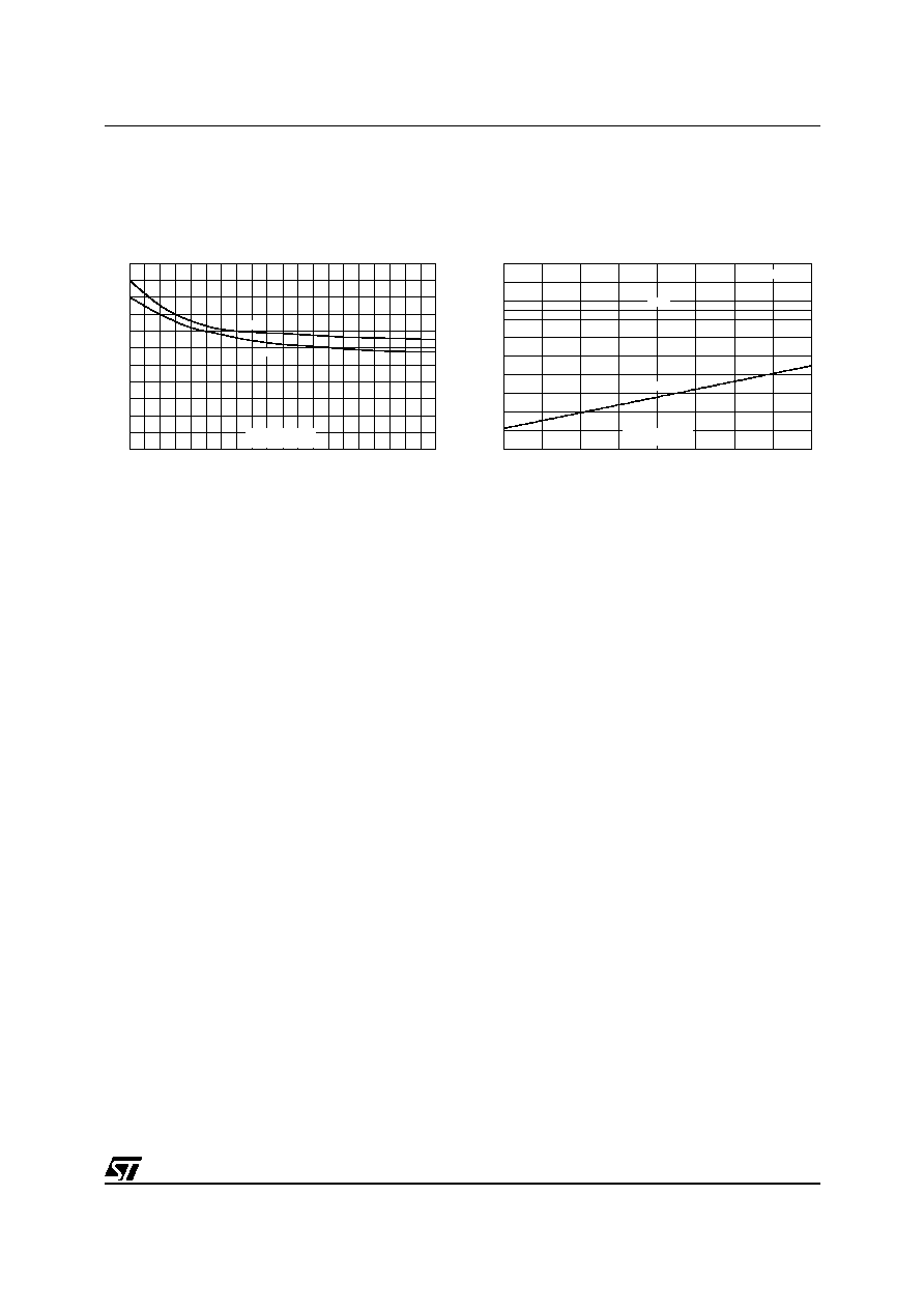
Figure 13: Thermal resistance junction to
ambient versus copper surface under lead
(epoxy FR4, e
CU
=35µm) (SMB / SMC)
Figure 14: Thermal resistance versus lead
length
0
10
20
30
40
50
60
70
80
90
100
110
0.0
0.5
1.0
1.5
2.0
2.5
3.0
3.5
4.0
4.5
5.0
S
(cm≤)
CU
R
(∞C/W)
th(j-a)
SMB
SMC
0
10
20
30
40
50
60
70
80
90
100
5
10
15
20
25
R (∞C/W)
th
L
(mm)
lead
R
th(j-a)
R
th(j-l)
DO-201AD