 | ÐлекÑÑоннÑй компоненÑ: STTH6004W | СкаÑаÑÑ:  PDF PDF  ZIP ZIP |
Äîêóìåíòàöèÿ è îïèñàíèÿ www.docs.chipfind.ru
®
1/6
Table 1: Main product characteristics
I
F(AV)
60 A
V
RRM
400 V
T
j
(max)
175 °C
V
F
(typ)
0.83 V
t
rr
(max)
50 ns
STTH6004W
Ultrafast high voltage rectifier
Table 3: Absolute ratings (limiting values)
Symbol
Parameter
Value
Unit
V
RRM
Repetitive peak reverse voltage
400
V
I
F(RMS)
RMS forward current
90
A
I
F(AV)
Average forward current
T
c
= 125 °C
= 0.5
60
A
I
FSM
Surge non repetitive forward current
t
p
= 10 ms sinusoidal
600
A
T
stg
Storage temperature range
-65 to + 175
°C
T
j
Maximum operating junction temperature
175
°C
K
A
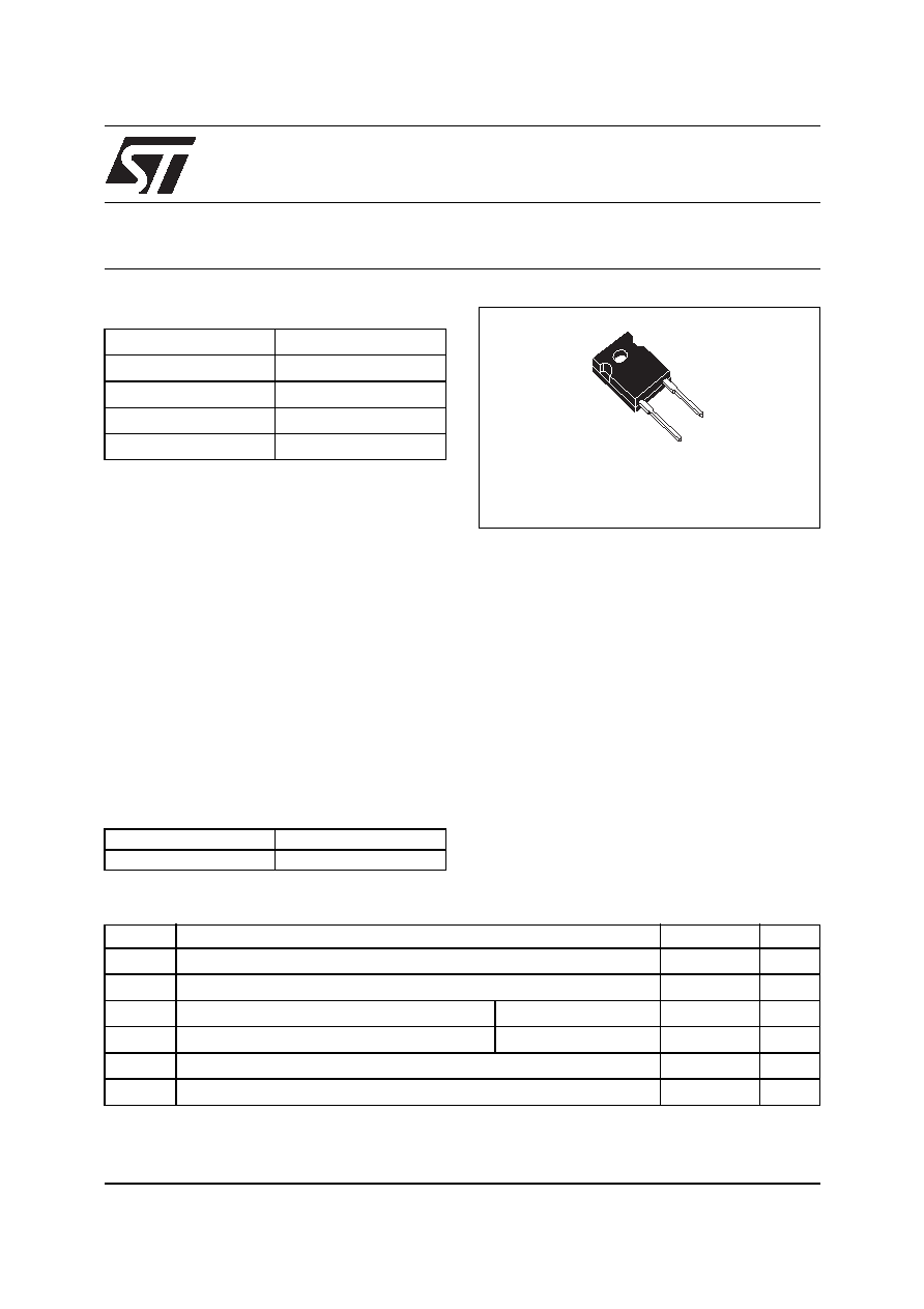
DO-247
STTH6004W
October 2005
REV. 1
Features and benefits
Ultrafast switching
Low reverse current
Low thermal resistance
Reduces switching & conduction losses
Description
The STTH6004W uses ST 400V technology and
is specially suited for use in switching power
supplies, welding equipment and industrial
applications, as an output rectification diode.
Table 2: Order codes
Part number
Marking
STTH6004W
STTH6004W
STTH6004W
2/6
Table 4: Thermal Resistance
Table 5: Static electrical characteristics
Pulse test:
* tp = 5 ms,
< 2%
** tp = 380 µs,
< 2%
To evaluate the conduction losses use the following equation: P = 0.8 x IF(AV) + 0.0033 IF
2
(RMS)
Table 6: Dynamic characteristics
Symbol
Parameter
Value (max).
Unit
R
th(j-c)
Junction to case
0.70
°C/W
Symbol
Parameter
Test conditions
Min.
Typ
Max.
Unit
I
R
*
Reverse leakage current T
j
= 25 °C
V
R
= V
RRM
50
µA
T
j
= 150 °C
100
1000
V
F
**
Forward voltage drop
T
j
= 25 °C
I
F
= 60 A
1.2
V
T
j
= 150 °C
0.83
1.0
Symbol
Parameter
Test conditions
Min
Typ Max Unit
t
rr
Reverse recovery
time
T
j
= 25 °C
I
F
= 1 A dI
F
/dt = 50 A/µs V
R
=30 V
66
90
ns
I
F
= 1 A dI
F
/dt = 200 A/µs V
R
=30 V
36
50
I
RM
Reverse recovery
current
T
j
= 125 °C I
F
= 60 A V
R
= 200 V
dI
F
/dt = 100 A/µs
15
A
S
factor
Softness factor
T
j
= 125 °C I
F
= 60 A V
R
= 200 V
dI
F
/dt = 100 A/µs
0.4
t
fr
Forward recovery
time
T
j
= 25 °C
I
F
= 60 A dI
F
/dt = 200 A/µs
V
FR
= 1.1 x V
Fmax
600
ns
V
FP
Forward recovery
voltage
T
j
= 25 °C
I
F
= 60 A dI
F
/dt = 200 A/µs
V
FR
= 1.1 x V
Fmax
3.2
V
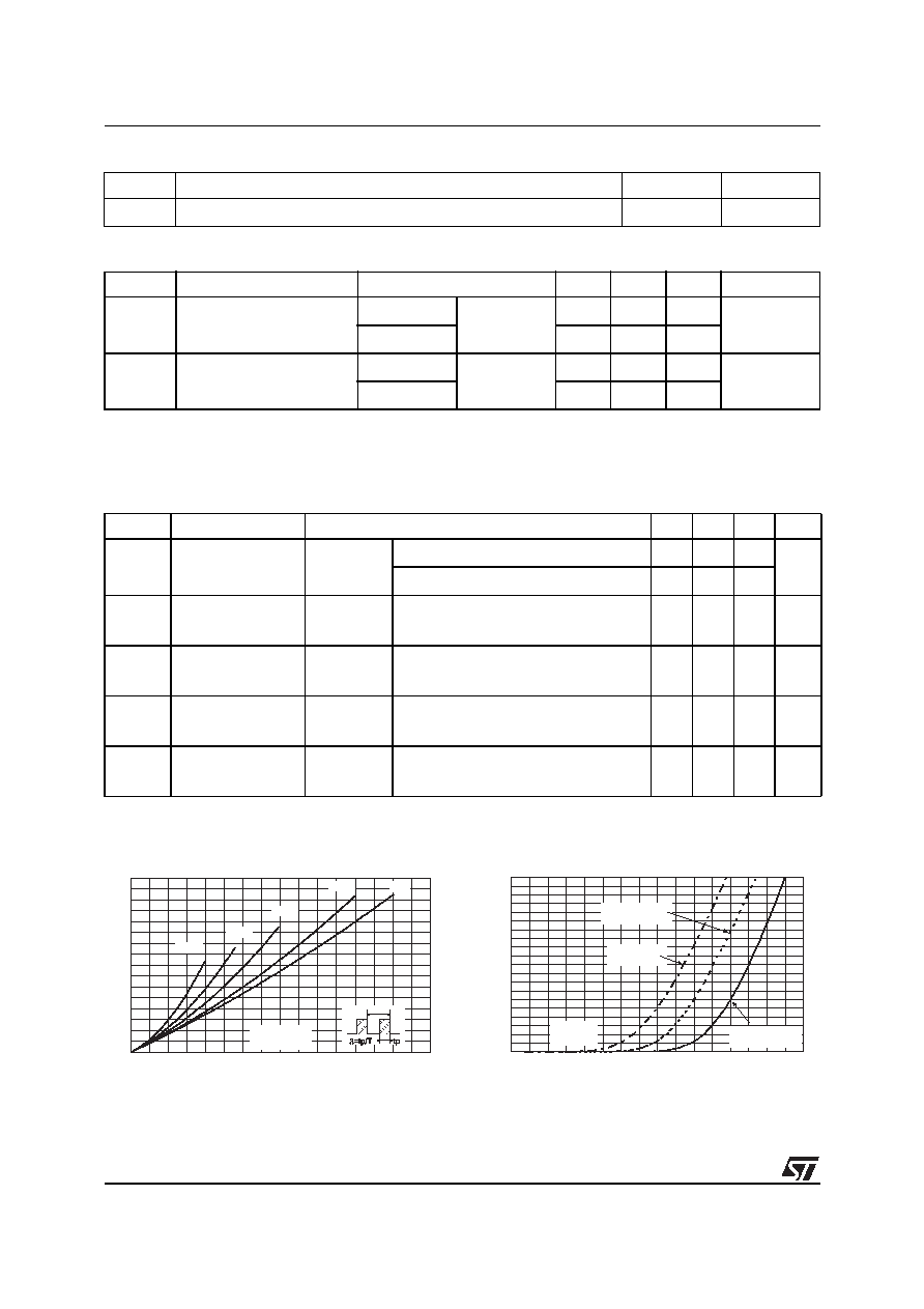
Figure 1: Conduction losses versus average
forward current
Figure 2: Forward voltage drop versus forward
current
0
10
20
30
40
50
60
70
80
0
10
20
30
40
50
60
70
80
P (W)
d=0.05
d=0.1
d=0.2
d=0.5
d=1
T
I
F(AV)
(A)
0
20
40
60
80
100
120
140
160
180
200
0.0
0.2
0.4
0.6
0.8
1.0
1.2
1.4
1.6
I
FM
(A)
T
J
=150°C
(Maximum values)
T
J
=150°C
(Typical values)
T
J
=25°C
(Maximum values)
V
FM
(V)
STTH6004W
3/6
Figure 3: Relative variation of thermal
impedance junction to case versus pulse
duration
Figure 4: Peak reverse recovery current versus
dI
F
/dt (typical values)
Figure 5: Reverse recovery time versus dI
F
/dt
(typical values)
Figure 6: Reverse recovery charges versus
dI
F
/dt (typical values)
Figure 7: Reverse recovery softness factor
versus dI
F
/dt (typical values)
Figure 8: Relative variations of dynamic
parameters versus junction temperature
0.0
0.1
0.2
0.3
0.4
0.5
0.6
0.7
0.8
0.9
1.0
1.E-04
1.E-03
1.E-02
1.E-01
1.E+00
Z th(j-c)/Rth(j-c)
Single pulse
t
P
(s)
0
5
10
15
20
25
30
35
40
45
0
50
100
150
200
250
300
350
400
450
500
I
RM
(A)
I
F
=I
F(AV)
V
R
=200V
T
j
=125°C
dIF /dt(A/µs)
0
50
100
150
200
250
300
0
50
100
150
200
250
300
350
400
450
500
t
(ns)
I
F
=I
F(AV)
V
R
=200V
T
j
=125°C
dIF /dt(A/µs)
rr
0
500
1000
1500
2000
2500
3000
0
100
200
300
400
500
Q
(nC)
I
F
=I
F(AV)
V
R
=200V
T
j
=125°C
dI F/dt(A/µs)
rr
0.0
0.1
0.2
0.3
0.4
0.5
0.6
0.7
0.8
0
50
100
150
200
250
300
350
400
450
500
SFACTOR
I
F
< 2 x I
F(AV)
V
R
=200V
T
j
=125°C
dI F /dt(A/µs)
0.0
0.2
0.4
0.6
0.8
1.0
1.2
1.4
1.6
25
50
75
100
125
I
RM
& t
RR
S
FACTOR
I
F
=I
F(AV)
V
R
=200V
Reference: T
j
=125°C
Q
RR
T
j
(°C)
STTH6004W
4/6
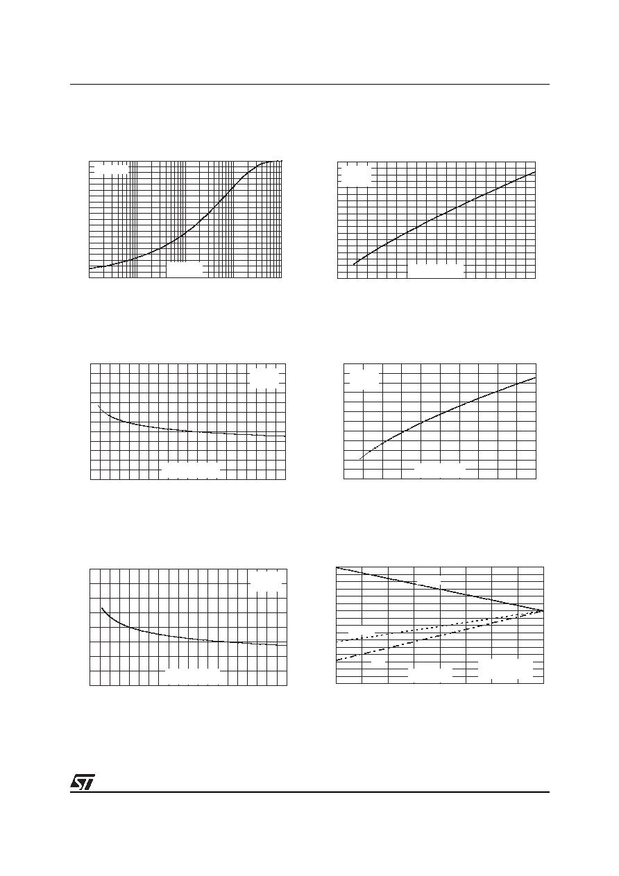
Figure 9: Transient peak forward voltage
versus dI
F
/dt (typical values)
Figure 10: Forward recovery time versus dI
F
/dt
(typical values)
Figure 11: Junction capacitance versus
reverse voltage applied (typical values)
0
1
2
3
4
5
6
7
8
0
50
100
150
200
250
300
350
400
450
500
VFP(V)
I
F
=I
F(AV)
T
j
=125°C
dI
F
/dt(A/µs)
0
100
200
300
400
500
600
700
800
900
1000
0
50
100
150
200
250
300
350
400
450
500
t
(ns)
I
F
=I
F(AV)
V
FR
=1.1 x V
F
max.
T
j
=125°C
dIF/dt(A/µs)
fr
100
1000
1
10
100
1000
C (pF)
F=1MHz
V
OSC
=30mV
RMS
T
j
=25°C
V
R
(V)
STTH6004W
5/6
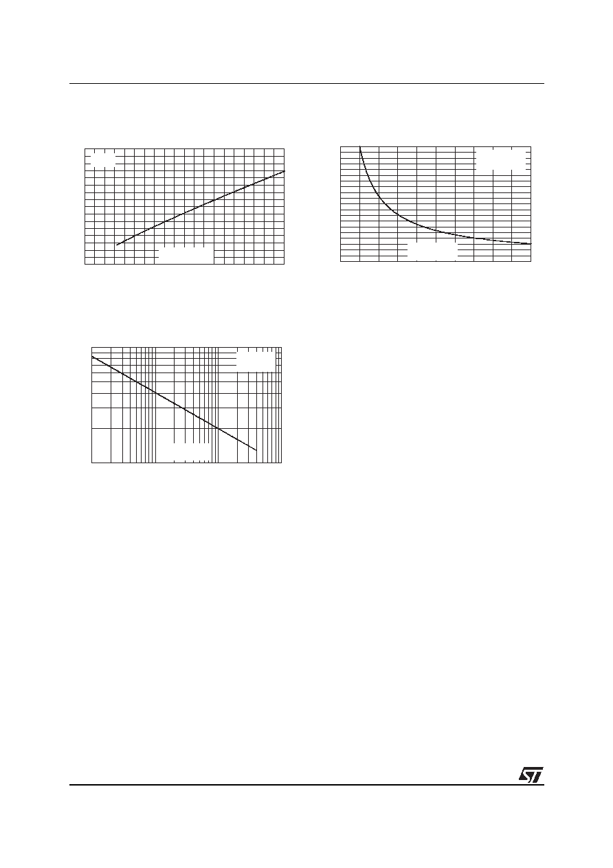
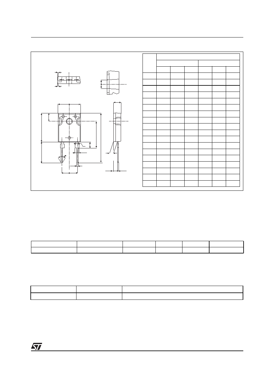
Figure 12: DO-247 Package mechanical data
In order to meet environmental requirements, ST offers these devices in ECOPACK® packages. These
packages have a Lead-free second level interconnect . The category of second level interconnect is
marked on the package and on the inner box label, in compliance with JEDEC Standard JESD97. The
maximum ratings related to soldering conditions are also marked on the inner box label. ECOPACK is an
ST trademark. ECOPACK specifications are available at: www.st.com.
V
H
L5
L
L3
V2
G
F
F3
L1
F2
L2
L4
V
Dia
A
D
M
E
Table 7: Ordering information
Epoxy meets UL94, V0
Cooling method: by conduction (C)
Recommended torque value: 0.8 Nm.
Maximum torque value: 1.0 Nm.
Ordering type
Marking
Package
Weight
Base qty
Delivery mode
STTH6004W
STTH6004W
DO-247
4.40 g
30
Tube
REF.
DIMENSIONS
Millimeters
Inches
Min.
Typ. Max. Min.
Typ. Max.
A
4.85
5.15 0.191
0.203
D
2.20
2.60 0.086
0.102
E
0.40
0.80 0.015
0.031
F
1.00
1.40 0.039
0.055
F2
2.00
0.078
F3
2.00
2.40 0.078
0.094
G
10.90
0.429
H
15.45
15.75 0.608
0.620
L
19.85
20.15 0.781
0.793
L1
3.70
4.30 0.145
0.169
L2
18.50
0.728
L3
14.20
14.80 0.559
0.582
L4
34.60
1.362
L5
5.50
0.216
M
2.00
3.00 0.078
0.118
V
5°
5°
V2
60°
60°
Dia.
3.55
3.65 0.139
0.143
Table 8: Revision history
Date
Revision
Description of Changes
18-Oct-2005
1
First issue