Äîêóìåíòàöèÿ è îïèñàíèÿ www.docs.chipfind.ru
®
1/6
Table 1: Main Product Characteristics
I
F(AV)
Up to 2 x 40 A
V
RRM
600 V
T
j
150°C
V
F
(typ)
1.0 V
t
rr
(max)
65 ns
STTH60L06TV
TURBO 2 ULTRAFAST HIGH VOLTAGE RECTIFIER
Table 3: Absolute Ratings (limiting values, per diode)
Symbol
Parameter
Value
Unit
V
RRM
Repetitive peak reverse voltage
600
V
I
F(RMS)
RMS forward voltage
100
A
I
F(AV)
Average forward current
= 0.5
Tc = 75°C
Per diode
30
A
Tc = 70°C
Per diode
40
I
FSM
Surge non repetitive forward current
tp = 10ms sinusoidal
210
A
T
stg
Storage temperature range
-55 to + 150
°C
T
j
Maximum operating junction temperature
150
°C
K1
K2
A2
A1
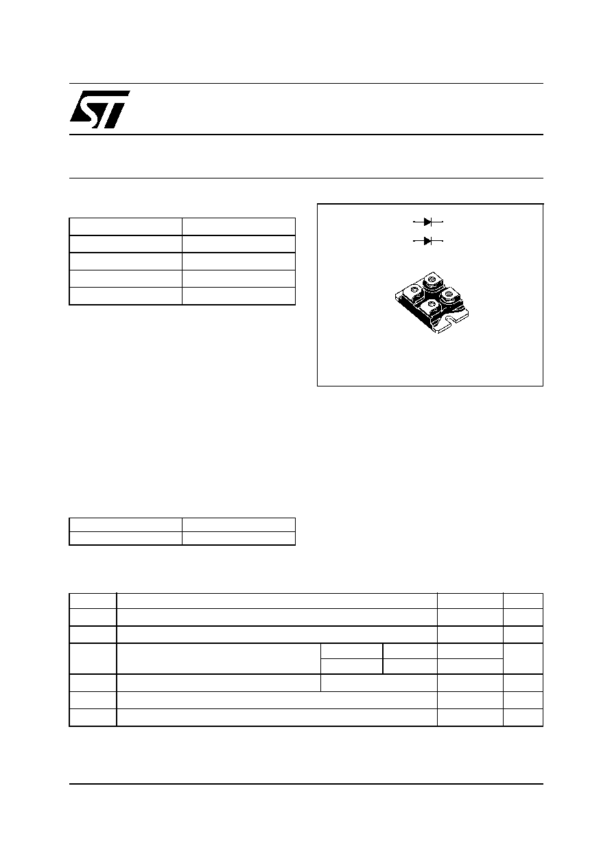
ISOTOP
STTH60L06TV1
A1
K1
A2
K2
September 2004
REV. 2
FEATURES AND BENEFITS
Ultrafast switching
Low reverse current
Low thermal resistance
Reduces switching & conduction losses
DESCRIPTION
The STTH60L06TV, which is using ST Turbo 2
600V technology, is specially suited for use in
switching power supplies, and industrial
applications (such as welding), as rectification
diode.
Table 2: Order Codes
Part Number
Marking
STTH60L06TV1
STTH60L06TV1

STTH60L06TV
2/6
Table 4: Thermal Resistance
Table 5: Static Electrical Characteristics (per diode)
Pulse test:
* tp = 5 ms,
< 2%
** tp = 380 µs,
< 2%
To evaluate the conduction losses use the following equation: P = 0.95 x I
F(AV)
+ 0.010 I
F
2
(RMS)
Table 6: Dynamic Characteristics (per diode)
Symbol
Parameter
Value (max).
Unit
R
th(j-c)
Junction to case
Per diode
1.60
°C/W
Total
0.85
R
th(c)
Coupling
0.1
°C/W
When the diodes 1 and 2 are used simultaneously:
Tj(diode 1) = P(diode 1) x R
th(j-c)
(Per diode) + P(diode 2) x R
th(c)
Symbol
Parameter
Test conditions
Min.
Typ
Max.
Unit
I
R
*
Reverse leakage current T
j
= 25°C
V
R
= V
RRM
25
µA
T
j
= 125°C
25
250
V
F
**
Forward voltage drop
T
j
= 25°C
I
F
= 30A
1.55
V
T
j
= 150°C
1.0
1.25
Symbol
Parameter
Test conditions
Min.
Typ Max.
Unit
t
rr
Reverse recovery
time
T
j
= 25°C
I
F
= 0.5A Irr = 0.25A I
R
=1A
65
ns
I
F
= 1A dI
F
/dt = 50 A/µs V
R
=30V
65
90
I
RM
Reverse recovery
current
T
j
= 125°C I
F
= 30A V
R
= 400V
dI
F
/dt = 100 A/µs
11.5
16
A
t
fr
Forward recovery
time
T
j
= 25°C
I
F
= 30A dI
F
/dt = 100 A/µs
V
FR
= 1.1 x V
Fmax
500
ns
V
FP
Forward recovery
voltage
T
j
= 25°C
I
F
= 30A dI
F
/dt = 100 A/µs
V
FR
= 1.1 x V
Fmax
2.5
V
STTH60L06TV
3/6
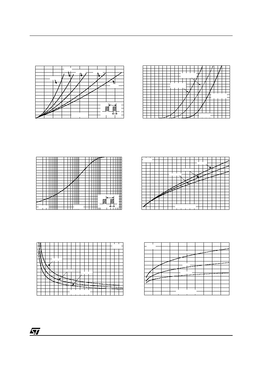
Figure 1: Conduction losses versus average
forward current (per diode)
Figure 2: Forward voltage drop versus forward
current (per diode)
Figure 3: Relative variation of thermal
impedance junction to case versus pulse
duration
Figure 4: Peak reverse recovery current versus
dI
F
/dt (typical values, per diode)
Figure 5: Reverse recovery time versus dI
F
/dt
(typical values, per diode)
Figure 6: Reverse recovery charges versus
dI
F
/dt (typical values, per diode)
0
10
20
30
40
50
60
70
80
0
10
20
30
40
50
P(W)
T
=tp/T
tp
= 1
= 0.05
I
(A)
F(AV)
= 0.1
= 0.2
= 0.5
0
10
20
30
40
50
60
70
80
90
100
0.0
0.2
0.4
0.6
0.8
1.0
1.2
1.4
1.6
1.8
2.0
2.2
I
(A)
FM
T =150°C
(typical values)
j
T =25°C
(maximum values)
j
V
(V)
FM
T =150°C
(maximum values)
j
0.0
0.1
0.2
0.3
0.4
0.5
0.6
0.7
0.8
0.9
1.0
1.E-03
1.E-02
1.E-01
1.E+00
1.E+01
Z
/R
th(j-c)
th(j-c)
t (s)
p
Single pulse
T
=tp/T
tp
0
5
10
15
20
25
30
35
40
45
0
50
100
150
200
250
300
350
400
450
500
I
(A)
RM
dI /dt(A/µs)
F
I =2 x I
F
F(AV)
I =I
F
F(AV)
I =0.5 x I
F
F(AV)
V =400V
T =125°C
R
j
0
100
200
300
400
500
600
700
800
0
50
100
150
200
250
300
350
400
450
500
t (ns)
rr
dI /dt(A/µs)
F
I =I
F
F(AV)
I =0.5 x I
F
F(AV)
V =400V
T =125°C
R
j
I =2 x I
F
F(AV)
0
500
1000
1500
2000
2500
3000
3500
0
100
200
300
400
500
Q (nC)
rr
I =2 x I
F
F(AV)
I =I
F
F(AV)
I =0.5 x I
F
F(AV)
V =400V
T =125°C
R
j
dI /dt(A/µs)
F
STTH60L06TV
4/6
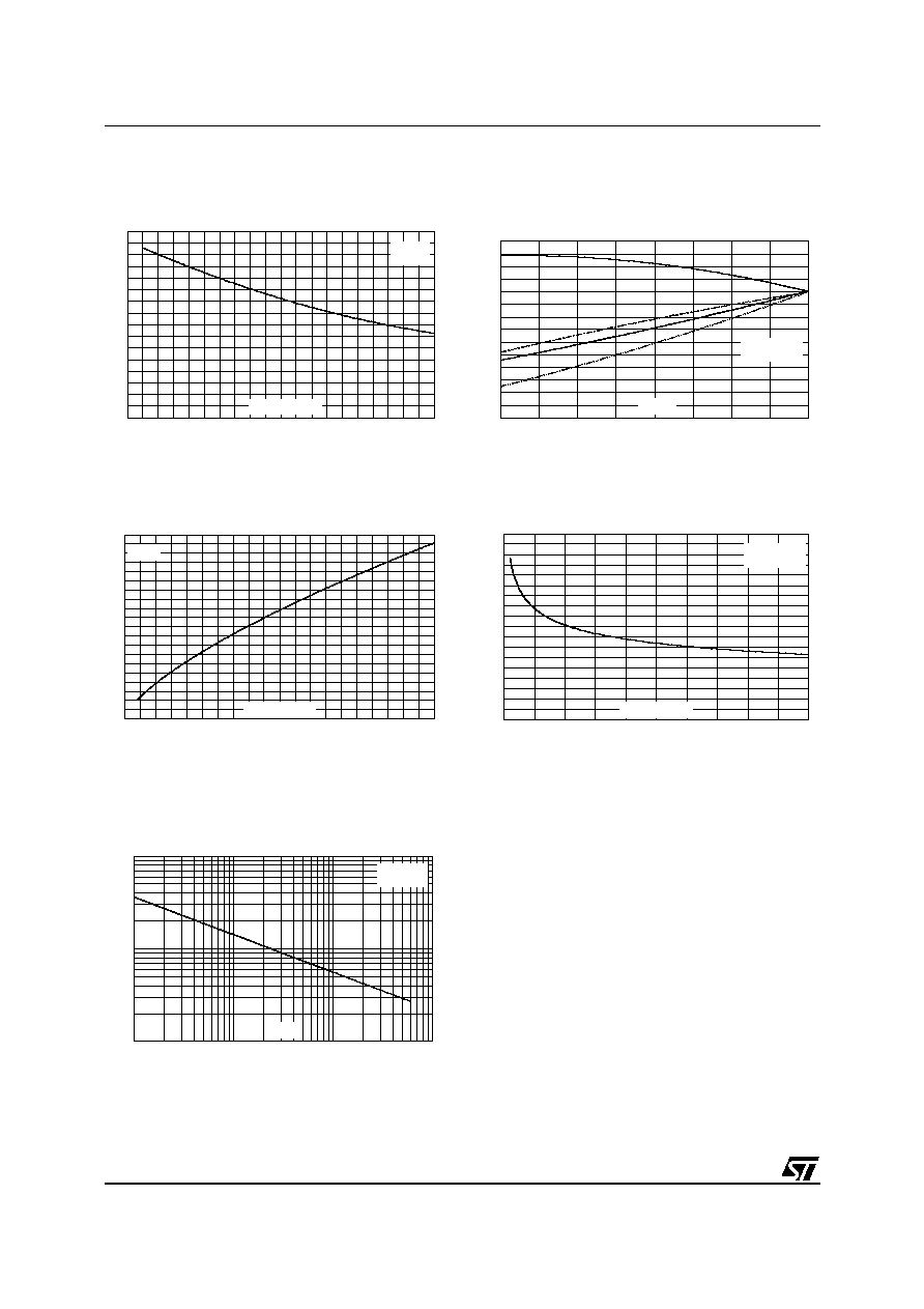
Figure 7: Reverse recovery softness factor
versus dI
F
/dt (typical values, per diode)
Figure 8: Relative variations of dynamic
parameters versus junction temperature
Figure 9: Transient peak forward voltage
versus dI
F
/dt (typical values, per diode)
Figure 10: Forward recovery time versus dI
F
/dt
(typical values, per diode)
Figure 11: Junction capacitance versus
reverse voltage applied (typical values, per
diode)
0.0
0.2
0.4
0.6
0.8
1.0
1.2
1.4
1.6
0
50
100
150
200
250
300
350
400
450
500
S factor
dI /dt(A/µs)
F
I < 2 x I
T =125°C
F
F(AV)
j
V =400V
R
0.0
0.2
0.4
0.6
0.8
1.0
1.2
1.4
25
50
75
100
125
I
RM
t
rr
S factor
T (°C)
j
I =I
Reference: T =125°C
F
F(AV)
j
V =400V
R
Q
RR
0
1
2
3
4
5
6
7
8
9
10
0
50
100
150
200
250
300
350
400
450
500
V
(V)
FP
dI /dt(A/µs)
F
I =I
T =125°C
F
F(AV)
j
0
50
100
150
200
250
300
350
400
450
0
100
200
300
400
500
t (ns)
fr
dI /dt(A/µs)
F
I =I
T =125°C
F
F(AV)
j
V
=1.1 x V max.
FR
F
10
100
1000
1
10
100
1000
C(pF)
V (V)
R
F=1MHz
V
=30mV
T =25°C
OSC
RMS
j
STTH60L06TV
5/6
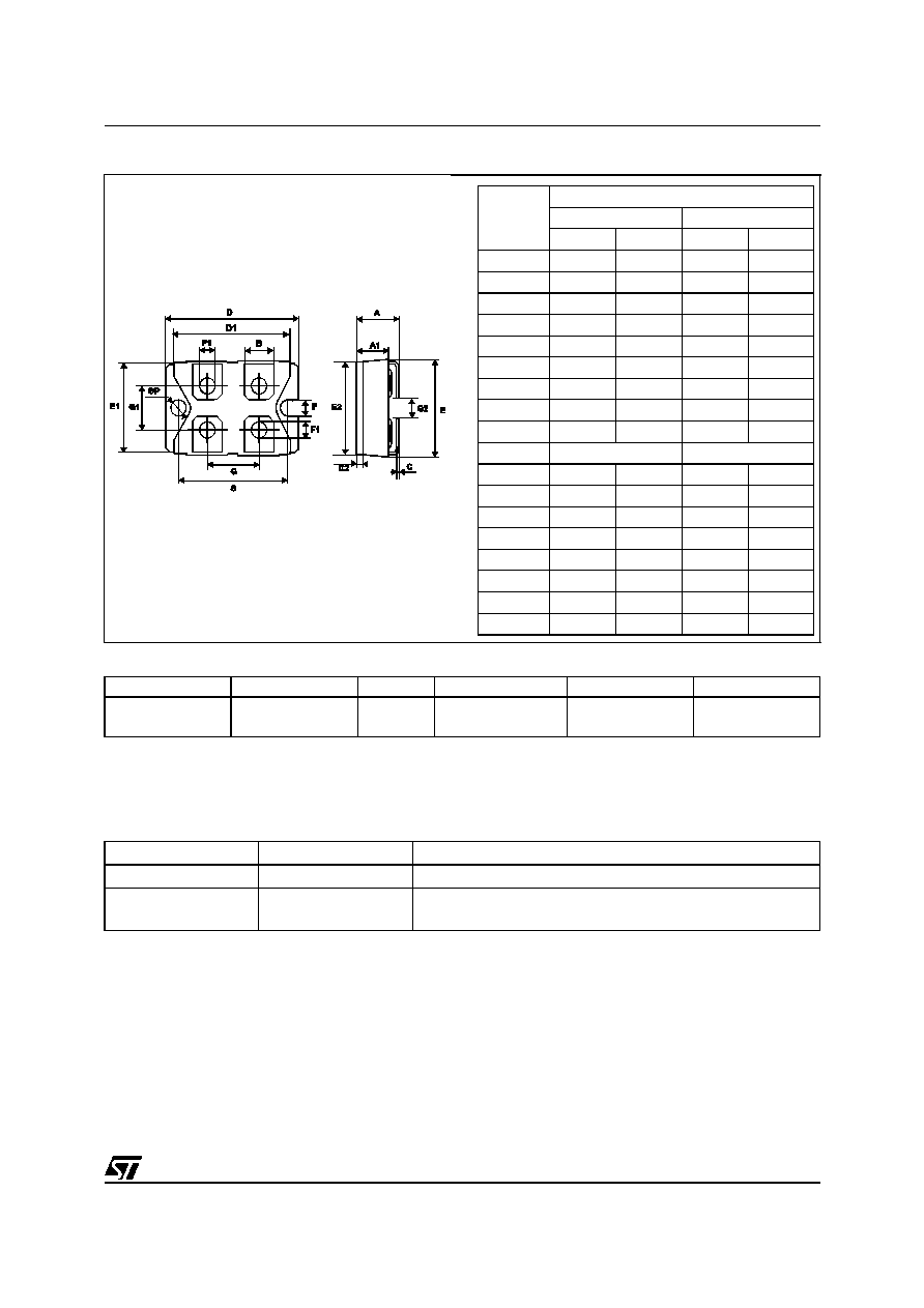
Figure 12: ISOTOP Package Mechanical Data
Table 7: Ordering Information
Epoxy meets UL94, V0
Cooling method: by conduction (C)
Ordering type
Marking
Package
Weight
Base qty
Delivery mode
STTH60L06TV1 STTH60L06TV1
ISOTOP
27 g
(without screws)
10
(with screws)
Tube
REF.
DIMENSIONS
Millimeters
Inches
Min.
Max.
Min.
Max.
A
11.80
12.20
0.465
0.480
A1
8.90
9.10
0.350
0.358
B
7.8
8.20
0.307
0.323
C
0.75
0.85
0.030
0.033
C2
1.95
2.05
0.077
0.081
D
37.80
38.20
1.488
1.504
D1
31.50
31.70
1.240
1.248
E
25.15
25.50
0.990
1.004
E1
23.85
24.15
0.939
0.951
E2
24.80 typ.
0.976 typ.
G
14.90
15.10
0.587
0.594
G1
12.60
12.80
0.496
0.504
G2
3.50
4.30
0.138
0.169
F
4.10
4.30
0.161
0.169
F1
4.60
5.00
0.181
0.197
P
4.00
4.30
0.157
0.69
P1
4.00
4.40
0.157
0.173
S
30.10
30.30
1.185
1.193
Table 8: Revision History
Date
Revision
Description of Changes
07-Sep-2004
1
First issue
10-Sep-2004
2
Average forward current (page 1) and Junction to case
(page 2) values changed