 | –≠–ª–µ–∫—Ç—Ä–æ–Ω–Ω—ã–π –∫–æ–º–ø–æ–Ω–µ–Ω—Ç: STTH8L06D | –°–∫–∞—á–∞—Ç—å:  PDF PDF  ZIP ZIP |
Æ
1/8
Table 1: Main Product Characteristics
I
F(AV)
8 A
V
RRM
600 V
I
R
(max)
200 µA
T
j
175∞C
V
F
(typ)
0.85 V
t
rr
(typ)
75 ns
STTH8L06
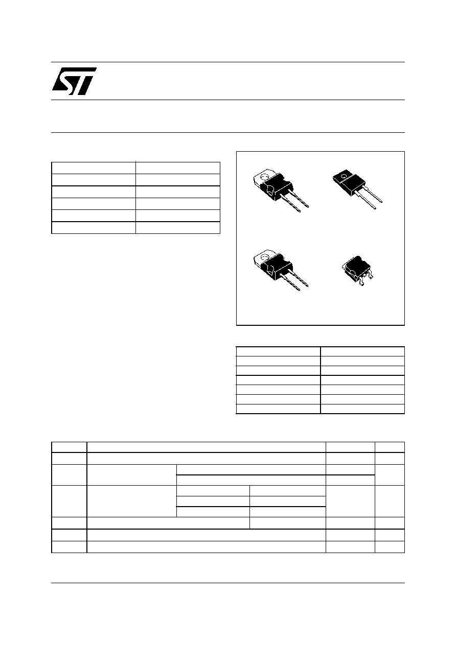
TURBO 2 ULTRAFAST HIGH VOLTAGE RECTIFIER
K
K
A
TO-220AC
STTH8L06D
K
A
TO-220FPAC
STTH8L06FP
K
A
TO-220AC Insulated
STTH8L06DI
K
A
NC
D
2
PAK
STTH8L06G
October 2004
REV. 3
FEATURES AND BENEFITS
Ultrafast switching
Low reverse recovery current
Low thermal resistance
Reduces switching and conduction losses
DESCRIPTION
The STTH8L06, which is using ST Turbo2 600V
technology, is specially suited as boost diode in
discontinuous or critical mode power factor
corrections.
The device is also intended for use as a free
wheeling diode in power supplies and other power
switching applications.
Table 2: Order Codes
Part Number
Marking
STTH8L06D
STTH8L06D
STTH8L06FP
STTH8L06FP
STTH8L06DI
STTH8L06DI
STTH8L06DIRG
STTH8L06DI
STTH8L06G
STTH8L06G
STTH8L06G-TR
STTH8L06G
Table 3: Absolute Ratings (limiting values)
Symbol
Parameter
Value
Unit
V
RRM
Repetitive peak reverse voltage
600
V
I
F(RMS)
RMS forward voltage
TO-220AC / TO-220FPAC
30
A
TO-220AC Ins.
24
I
F(AV)
Average forward current
= 0.5
TO-220AC
Tc = 150∞C
8
A
TO-220FPAC
Tc = 125∞C
TO-220AC Ins.
Tc = 135∞C
I
FSM
Surge non repetitive forward current
tp = 10ms sinusoidal
120
A
T
stg
Storage temperature range
-65 to + 175
∞C
T
j
Maximum operating junction temperature
175
∞C
STTH8L06
2/8
Table 4: Thermal Resistance
Table 5: Static Electrical Characteristics
To evaluate the conduction losses use the following equation: P = 0.89 x IF(AV) + 0.022 IF
2
(RMS)
Table 6: Dynamic Characteristics
Symbol
Parameter
Value (max).
Unit
R
th(j-c)
Junction to case
TO-220AC / D
2
PAK
2.5
∞C/W
TO-220FPAC
5
TO-220AC Ins.
4
Symbol
Parameter
Test conditions
Min.
Typ
Max.
Unit
I
R
Reverse leakage current T
j
= 25∞C
V
R
= V
RRM
8
µA
T
j
= 150∞C
16
200
V
F
Forward
voltage
drop
T
j
= 25∞C
I
F
= 8A
1.3
V
T
j
= 150∞C
0.85
1.05
Symbol
Parameter
Test conditions
Min.
Typ Max.
Unit
t
rr
Reverse recovery
time
T
j
= 25∞C
I
F
= 1A dI
F
/dt = 50 A/µs V
R
=30V
75
105
ns
t
fr
Forward recovery
time
T
j
= 25∞C
I
F
= 8A dI
F
/dt = 100 A/µs
V
FR
= 1.1 x V
Fmax
150
ns
V
FP
Forward recovery
voltage
I
F
= 8A dI
F
/dt = 100 A/µs
6
V
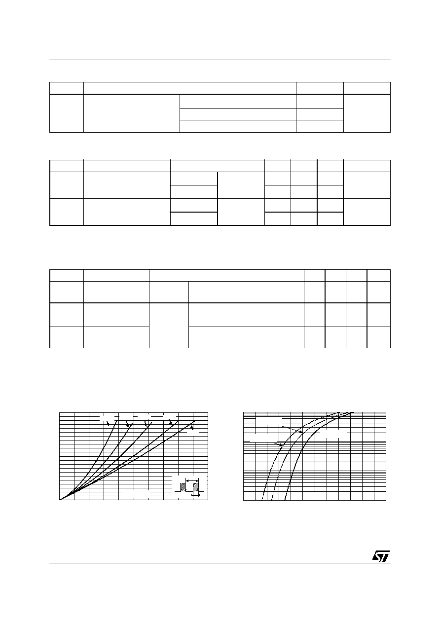
Figure 1: Conduction losses versus average
current
Figure 2: Forward voltage drop versus forward
current
0
1
2
3
4
5
6
7
8
9
10
11
0
2
4
6
8
10
T
=tp/T
tp
= 0.2
= 1
= 0.05
= 0.1
= 0.5
I
(A)
F(AV)
P(W)
0.1
1.0
10.0
100.0
0.0
0.5
1.0
1.5
2.0
2.5
3.0
I
(A)
FM
V
(V)
FM
T =25∞C
(maximum values)
j
T =150∞C
(maximum values)
j
T =150∞C
(typical values)
j
STTH8L06
3/8
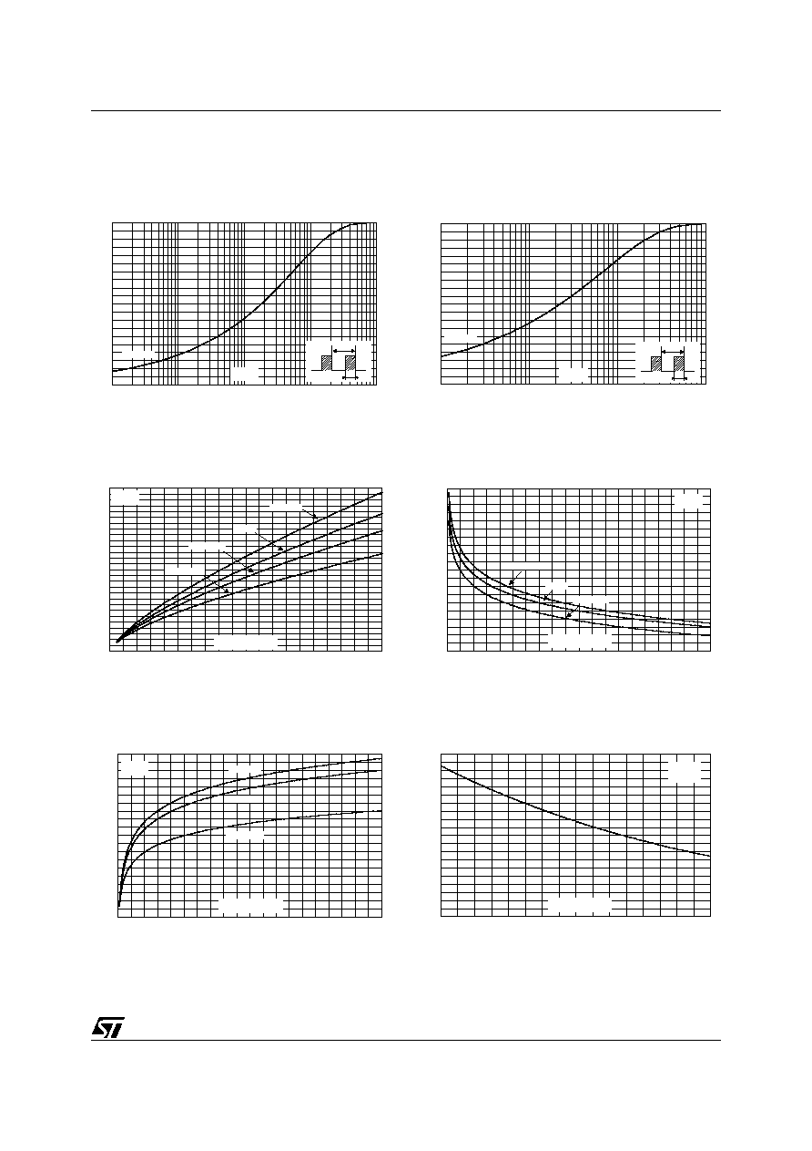
Figure 3: Relative variation of thermal
impedance junction to case versus pulse
duration (TO-220FPAC)
Figure 4: Relative variation of thermal
impedance junction to case versus pulse
duration (TO-220AC, TO-220AC Ins., D
2
PAK)
Figure 5: Peak reverse recovery current versus
dI
F
/dt (typical values)
Figure 6: Reverse recovery time versus dI
F
/dt
(typical values)
Figure 7: Reverse recovery charges versus dI
F
/dt
(typical values)
Figure 8: Softness factor versus dI
F
/dt (typical
values)
0.0
0.1
0.2
0.3
0.4
0.5
0.6
0.7
0.8
0.9
1.0
1.E-03
1.E-02
1.E-01
1.E+00
1.E+01
T
=tp/T
tp
Z
/R
th(j-c)
th(j-c)
t (s)
p
Single pulse
0.0
0.1
0.2
0.3
0.4
0.5
0.6
0.7
0.8
0.9
1.0
1.E-03
1.E-02
1.E-01
1.E+00
Z
/R
th(j-c)
th(j-c)
T
=tp/T
tp
t (s)
p
Single pulse
0
1
2
3
4
5
6
7
8
9
10
11
12
13
14
0
20
40
60
80
100
120
140
160
180
200
I
(A)
RM
dI /dt(A/µs)
F
I =2 x I
F
F(AV)
I =I
F
F(AV)
I =0.5 x I
F
F(AV)
I =0.25 x I
F
F(AV)
V =400V
T =125∞C
R
j
0
100
200
300
400
500
600
700
800
900
1000
0
20
40
60
80
100
120
140
160
180
200
t (ns)
rr
dI /dt(A/µs)
F
V =400V
T =125∞C
R
j
I =2 x I
F
F(AV)
I =I
F
F(AV)
I =0.5 x I
F
F(AV)
0
100
200
300
400
500
600
700
800
900
1000
0
20
40
60
80
100
120
140
160
180
200
Q (nC)
rr
I =2 x I
F
F(AV)
I =I
F
F(AV)
I =0.5 x I
F
F(AV)
V =400V
T =125∞C
R
j
dI /dt(A/µs)
F
0.0
0.2
0.4
0.6
0.8
1.0
1.2
1.4
1.6
1.8
2.0
0
25
50
75
100
125
150
175
200
S factor
I
2 x I
T =125∞C
F
F(AV)
j
V =400V
R
dI /dt(A/µs)
F
STTH8L06
4/8
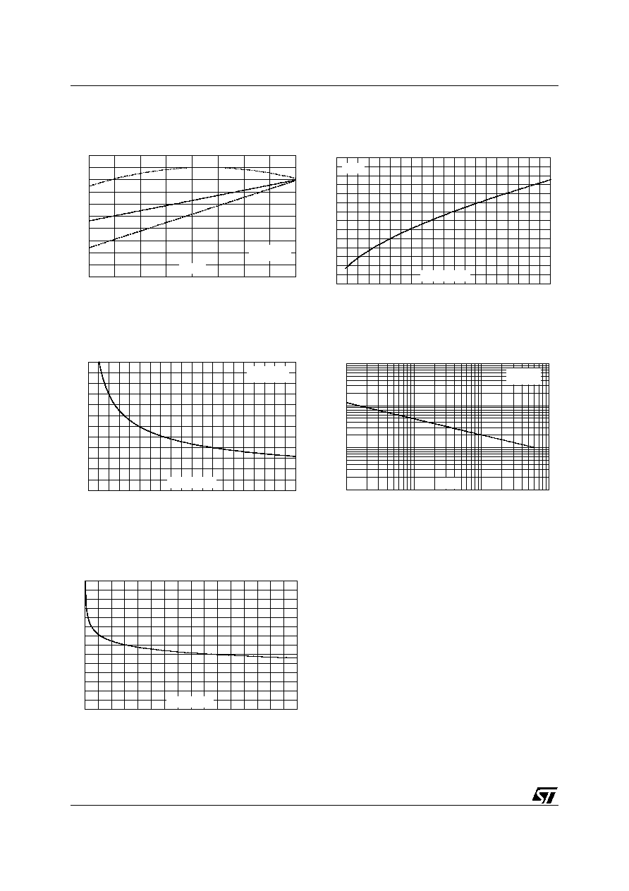
Figure 9: Relative variations of dynamic
parameters versus junction temperature
Figure 10: Transient peak forward voltage
versus dI
F
/dt
Figure 11: Forward recovery time versus dI
F
/dt
(typical values)
Figure 12: Junction capacitance versus
reverse voltage applied (typical values)
Figure 13: Thermal resistance junction to
ambient versus copper surface under tab
(epoxy FR4, e
CU
=35µm) (D
2
PAK)
0.00
0.25
0.50
0.75
1.00
1.25
25
50
75
100
125
I
RM
Q
RR
S factor
T (∞C)
j
I
2 x I
Reference: T =125∞C
F
F(AV)
j
V =400V
R
0
1
2
3
4
5
6
7
0
20
40
60
80
100
120
140
160
180
200
V
(V)
FP
dI /dt(A/µs)
F
I =I
T =125∞C
F
F(AV)
j
0
50
100
150
200
250
300
0
20
40
60
80
100
120
140
160
180
200
t (ns)
fr
dI /dt(A/µs)
F
I =I
T =125∞C
F
F(AV)
j
V
=1.1 x V max.
FR
F
1
10
100
1000
1
10
100
1000
C(pF)
V (V)
R
F=1MHz
V
=30mV
T =25∞C
OSC
RMS
j
0
10
20
30
40
50
60
70
0
5
10
15
20
25
30
35
40
S(Cu)(cm≤)
R
(∞C/W)
th(j-a)
STTH8L06
5/8
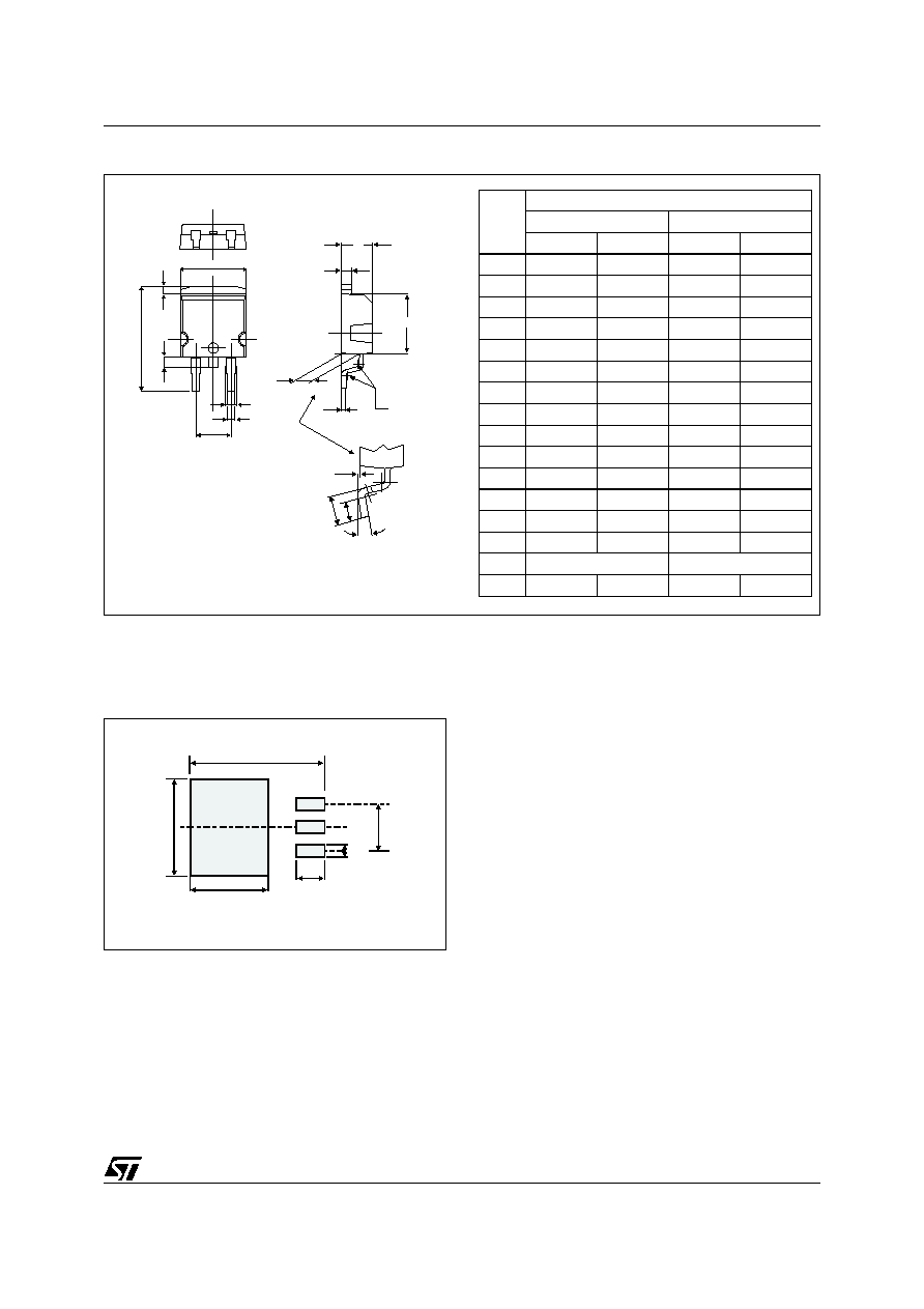
Figure 14: D
2
PAK Package Mechanical Data
Figure 15: D
2
PAK Foot Print Dimensions
(in millimeters)
A
C2
D
R
A2
M
V2
C
A1
G
L
L3
L2
B
B2
E
*
* FLAT ZONE NO LESSTHAN 2mm
REF.
DIMENSIONS
Millimeters
Inches
Min.
Max.
Min.
Max.
A
4.40
4.60
0.173
0.181
A1
2.49
2.69
0.098
0.106
A2
0.03
0.23
0.001
0.009
B
0.70
0.93
0.027
0.037
B2
1.14
1.70
0.045
0.067
C
0.45
0.60
0.017
0.024
C2
1.23
1.36
0.048
0.054
D
8.95
9.35
0.352
0.368
E
10.00
10.40
0.393
0.409
G
4.88
5.28
0.192
0.208
L
15.00
15.85
0.590
0.624
L2
1.27
1.40
0.050
0.055
L3
1.40
1.75
0.055
0.069
M
2.40
3.20
0.094
0.126
R
0.40 typ.
0.016 typ.
V2
0∞
8∞
0∞
8∞
8.90
3.70
1.30
5.08
16.90
10.30