 | –≠–ª–µ–∫—Ç—Ä–æ–Ω–Ω—ã–π –∫–æ–º–ø–æ–Ω–µ–Ω—Ç: STUSB02E | –°–∫–∞—á–∞—Ç—å:  PDF PDF  ZIP ZIP |
Document Outline
- 1 Pin Configuration
- Figure 1. Pin Connections (Top View )
- Table 1. Pin Description
- 2 Functional Tables
- Table 2. Function Selection
- Table 3. Truth Table During Normal Mode
- 3 Maximum Ratings
- Table 4. Absolute Maximum Ratings
- Table 5. Thermal Data
- 4 Electrical Characteristics
- Table 6. DC Electrical Characteristics (System and USB Interface) (VIF = 3.6V, VBUS = 5V unless otherwise noted; TA = 25�C, specifications over temperature, -40 to 85�C)
- Table 7. DC Electrical Characteristics (System and USB Interface) (VIF = 3.6V, VBUS = 5V unless otherwise noted; TA = 25�C)
- Table 8. ESD Performance
- Table 9. DC Electrical Characteristics (Transceiver) (VIF = 3.6V, VBUS = 5V unless otherwise noted; TA = 25�C, specifications over temperature, -40 to 85�C)
- Table 10. DC Electrical Characteristics (Transceiver) (VIF = 3.6V, VBUS = 5V unless otherwise noted; TA = 25�C)
- Table 11. AC Electrical Characteristics (VIF = 3.6V, VBUS = 5V unless otherwise noted; TA = 25�C.) (Note 6)
- 5 Timing Diagram
- Figure 2. Enable and Disable Times
- Figure 3. Rise and Fall Times
- Figure 4. Receiver Propagation Delay
- Figure 5. Driver Propagation Delay (CL = 50pF)
- Figure 6. Enable and Disable Time Circuit
- 6 Test Circuits
- Figure 7. Load for VP, VM, RCV
- Figure 8. Load for D+, D-
- Figure 9. Functional Diagram
- 7 Functional Description
- 8 Package Mechanical Data
- 9 Revision History

October 2005
1/20
20
Rev. 1
STUSB02E
USB Transceiver
Features
I
Compliant to USB v2.0 for Full-speed (12Mb/s)
and Low-speed (1.5Mbps) Operation
I
±14KV on D+, D≠ Lines; ±5KV on VBUS
I
ESD Compliant To IEC-61000-4.2 (Level 3)
I
Separate I/o Supply With Operation Down To
1.6V
I
Integrated Speed Select Termination Supply
I
Very Low Power Consumption To Meet USB
`suspend' Current Requirements
I
Small QFN16 Lead Free Package
I
No Power Supply Sequencing Requirements
I
Software Controlled Re-enumeration
Description
The STUSB02E is a single chip transceiver that
complies with the physical layer specifications of
the Universal Serial Bus (USB) v2.0 standard. It
has an integrated 5V to 3.3V regulator which
allows direct powering from the VBUS. The
transceiver has an integrated voltage detector to
detect the presence of the VBUS voltage.
The transceiver also supports Sharing mode
when VBUS is not present, which allows the D+/
D≠ lines to be shared with other serial protocols.
It supports both full-speed (12Mbps) and low-
speed (1.5Mbps) operation. It is also designed to
operate down to 1.6V so that it is compatible with
lower system voltages of most portable systems,
which include PDAs, MP3 Player and Cell phones
to mention few.
www.st.com
QFN16(3mmx3mm)
Order Codes
Typical Application
Type
Package
Comments
STUSB02EQR
QFN16 (3mm x 3mm)
3000 parts per reel

STUSB02E
2/20
Contents
1
Pin Configuration . . . . . . . . . . . . . . . . . . . . . . . . . . . . . . . . . . . . . . . . . . . . . . 3
2
Functional Tables . . . . . . . . . . . . . . . . . . . . . . . . . . . . . . . . . . . . . . . . . . . . . . 4
3
Maximum Ratings . . . . . . . . . . . . . . . . . . . . . . . . . . . . . . . . . . . . . . . . . . . . . 5
4
Electrical Characteristics . . . . . . . . . . . . . . . . . . . . . . . . . . . . . . . . . . . . . . . 6
5
Timing Diagram . . . . . . . . . . . . . . . . . . . . . . . . . . . . . . . . . . . . . . . . . . . . . . 10
6
Test Circuits . . . . . . . . . . . . . . . . . . . . . . . . . . . . . . . . . . . . . . . . . . . . . . . . . 12
7
Functional Description . . . . . . . . . . . . . . . . . . . . . . . . . . . . . . . . . . . . . . . . 14
8
Package Mechanical Data . . . . . . . . . . . . . . . . . . . . . . . . . . . . . . . . . . . . . . 15
9
Revision History . . . . . . . . . . . . . . . . . . . . . . . . . . . . . . . . . . . . . . . . . . . . . 18
STUSB02E
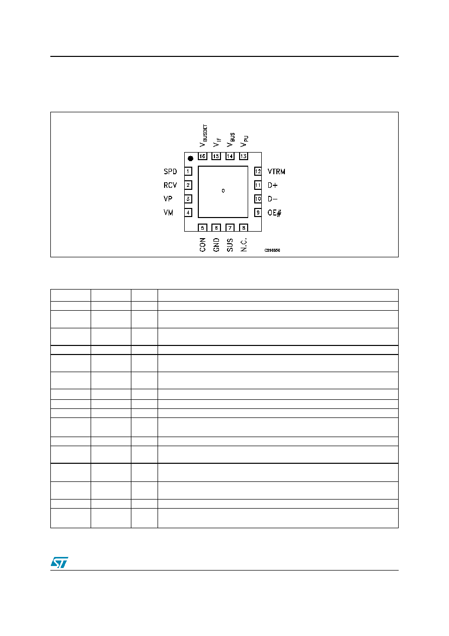
1 Pin Configuration
3/20
1
Pin Configuration
Table 1.
Pin Description
Figure 1.
Pin Connections (Top View )
PlN N∞
SYMBOL
I/O
NAME AND FUNCTION
0
N.C.
Not Connected.
15
V
IF
I
System Interface Supply Voltage (1.6V to 3.6V). (return) Provides reference
supply voltage for system I/O interface signals.
1
SPD
I
Edge Rate Control. A logic HIGH operates at edge rates for "fullspeed"
operation. A logic LOW operates edge rates for "lowspeed" operation.
2
RCV
O
Receive Data. Output for USB differential data. (see
Table 2
)
3
VP
I/O
If OE# = H, VP = Receiver output (+)
If OE# = L, VP = Driver input (+) (see
Table 2
)
4
VM
I/O
If OE# = H, VM = Receiver output (-)
If OE# = L, VM = Driver input (-) (see
Table 2
)
5
CON
I
CONNECT (input). Controls state of V
PU
. Refer to V
PU
pin description for detail.
6
GND
Ground Reference
7
SUS
I
Suspend (active-high). Turns off internal circuits to reduce supply current.
9
OE#
I
Output Enable (active-low). Enables transceiver data transmission onto the bus.
When not active, the transceiver is in the receive mode.
(see
Table 2
)
10, 11
D-, D+
I/O
Differential data lines that conform to the USB v2.0 standard. (see
Table 2
)
12
VTRM
O
3.3V Reference Supply Output. Requires a 1.0µF decoupling capacitor for
stability.
13
V
PU
O
Pull-up Supply Voltage Output. Used to connect 1.5K pull-up speed detect
resistor. If CON = 0, V
PU
is high impedance. If CON = 1, V
PU
= 3.3V ±10%.
14
V
BUS
I
USB Bus Supply Voltage (4V to 5.5V). Supplies power to the USB transceiver
and internal circuitry.
8
N.C.
Not connected.
16
V
BUSDET
O
V
BUS
indicator output. When V
BUS
> 2.9V, V
BUSDET
= High and when < 2.2V,
V
BUDET
= Low.
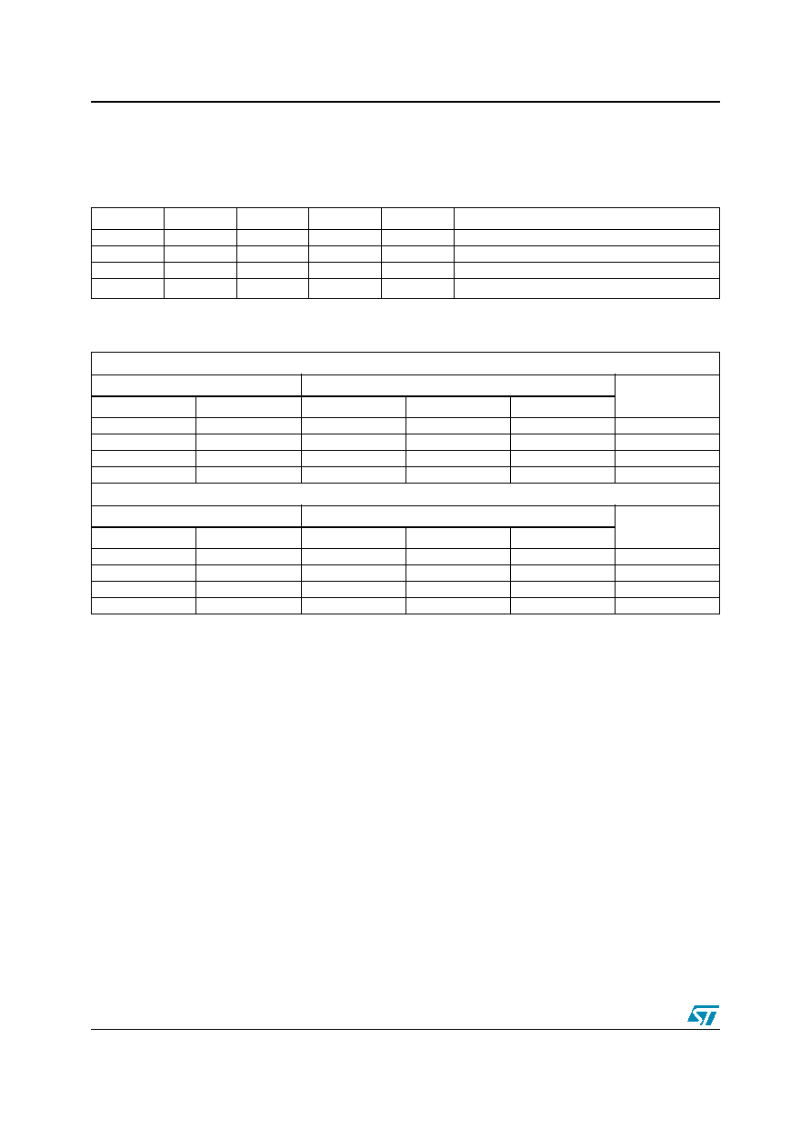
2 Functional Tables
STUSB02E
4/20
2 Functional
Tables
Table 2.
Function Selection
(1) During suspend VP and VM are active in order to detect out of band signalling conditions
Table 3.
Truth Table During Normal Mode
X = Undefined
SUS
OE#
D+, D-
RCV
VP/VM
FUNCTION
L
L
Driving
Active
Active
Normal transmit mode
L
H
Receiving
Active
Active
Normal receive mode
H
L
Hi-Z
L
Not Active Low power state
H
H
Hi-Z
L
Active
Receiving during suspend (low power state)
(1)
OE# = L
INPUT
OUTPUT
RESULT
VP
VM
D+
D-
RCV
L
L
L
L
X
SE0
L
H
L
H
L
Logic Low
H
L
H
L
H
Logic High
H
H
X
X
X
Undefined
OE# = H
INPUT
OUTPUT
RESULT
D+
D-
VP
VM
RCV
L
L
L
L
X
SE0
L
H
L
H
L
Logic Low
H
L
H
L
H
Logic High
H
H
X
X
X
Undefined

STUSB02E
3 Maximum Ratings
5/20
3 Maximum
Ratings
Table 4.
Absolute Maximum Ratings
Absolute Maximum Ratings are those values beyond which damage to the device may occur. Functional Operation under these con-
ditions is not implied.
Note 3. Devices are ESD sensitive. Handling precautions recommended. Human body model, 1.5k in series with 100pF.
Table 5.
Thermal Data
Symbol
Parameter
Value
Unit
V
BUS
Supply Voltage
6
V
V+
All other Inputs
-0.5 to 4.6
V
I
O
Output Current (D+, D-)
±
50
mA
I
O
Output Current (all others)
±
15
mA
I
I
Input Current
±
50
mA
ESD
D+, D-, HBM (Note 3)
±
14
KV
V
BUS
(Note 3)
±
5
All other pins (Note 3)
±
2
T
STG
Storage Temperature Range
-65 to + 150
∞C
T
OPR
Operating Temperature Range
-40 to + 85
∞C
Symbol
Parameter
Value
Unit
R
thJA
Thermal Resistance Junction-Ambient
59
∞C/W