 | –≠–ª–µ–∫—Ç—Ä–æ–Ω–Ω—ã–π –∫–æ–º–ø–æ–Ω–µ–Ω—Ç: STV0042 | –°–∫–∞—á–∞—Ç—å:  PDF PDF  ZIP ZIP |
STV0042A
SATELLITE SOUND AND VIDEO PROCESSORS
March 1997
PRODUCT PREVIEW
SHRINK42
(Plastic Package)
ORDER CODE : STV0042A
SOUND
.
TWO INDEPENDENT SOUND DEMODULATORS
.
PL L
DEMODULATION
WITH
5-10MHz
FREQUENCY SYNTHESIS
.
PROGRAMMABLE
FM
DEMODULATOR
BANDWIDTH ACCOMODATING FM DEVIA-
TIONS FROM
±
30kHz TILL
±
400kHz
.
PROGRAMMABLE 50/75
µ
s OR NO DE-EM-
PHASIS
.
DYNAMIC NOISE REDUCTION
.
ONE OR TWO AUXILIARY AUDIO INPUTS
AND OUTPUTS
.
GAIN
CONTROLLED
AND
MUTEABLE
AUDIO OUTPUTS
.
HIGH IMPEDANCE MODE AUDIO OUTPUTS
FOR TWIN TUNER APPLICATIONS
VIDEO
.
COMPOSITE VIDEO 6-bit 0 to 12.7dB GAIN
CONTROL
.
COMPOSITE
VIDEO
SELECTABLE
IN-
VERTER
.
TWO SELECTABLE VIDEO DE-EMPHASIS
NETWORKS
.
4 x 2 VIDEO MATRIX
.
HIGH IMPEDANCE MODE VIDEO OUTPUTS
FOR TWIN TUNER APPLICATIONS
MISCELLANEOUS
.
22kHz TONE GENERATION FOR LNB CONTROL
.
I
2
C BUS CONTROL :
CHIP ADDRESSES = 06
HEX
.
LOW POWER STAND-BY MODE WITH ACTIVE
AUDIO AND VIDEO MATRIXES
DESCRIPTION
The STV0042A BICMOS integrated circuit realizes
all the necessary signal processing from the tuner
to the Audio/Video input and output connectors
regardless the satellite system.
The STV0042 is intended for low cost satellite
receiver application.
1
2
3
4
5
6
7
8
9
10
11
12
13
14
15
16
17
18
19
20
21
22
23
24
25
26
27
28
29
30
31
32
33
34
35
36
37
38
39
40
41
42
A GND R
FC L
PK OUT
I
REF
CPUMP R
U75 R
DET R
AMPLK R
A 12V
A 12V
V
REF
A GND L
AGC R
AMPLK L
U75 L
DET L
CPUMP L
GND 5V
V
DD
5V
XTL
SDA
SCL
AGC L
FM IN
S2 RTN R
S2 RTN L
B-BAND IN
V GND
CLAMP IN
VIDEEM1
V 12V
VIDEEM2/22kHz
UNCL DEEM
S2 OUT R
S2 OUT L
S2 VID RTN
VOL L
S2 VID OUT
S1 VID OUT
VOL R
SUM OUT
PK IN
FC R
0042A
-
0
1
.
E
P
S
PIN CONNECTIONS
1/24
PIN ASSIGNMENT
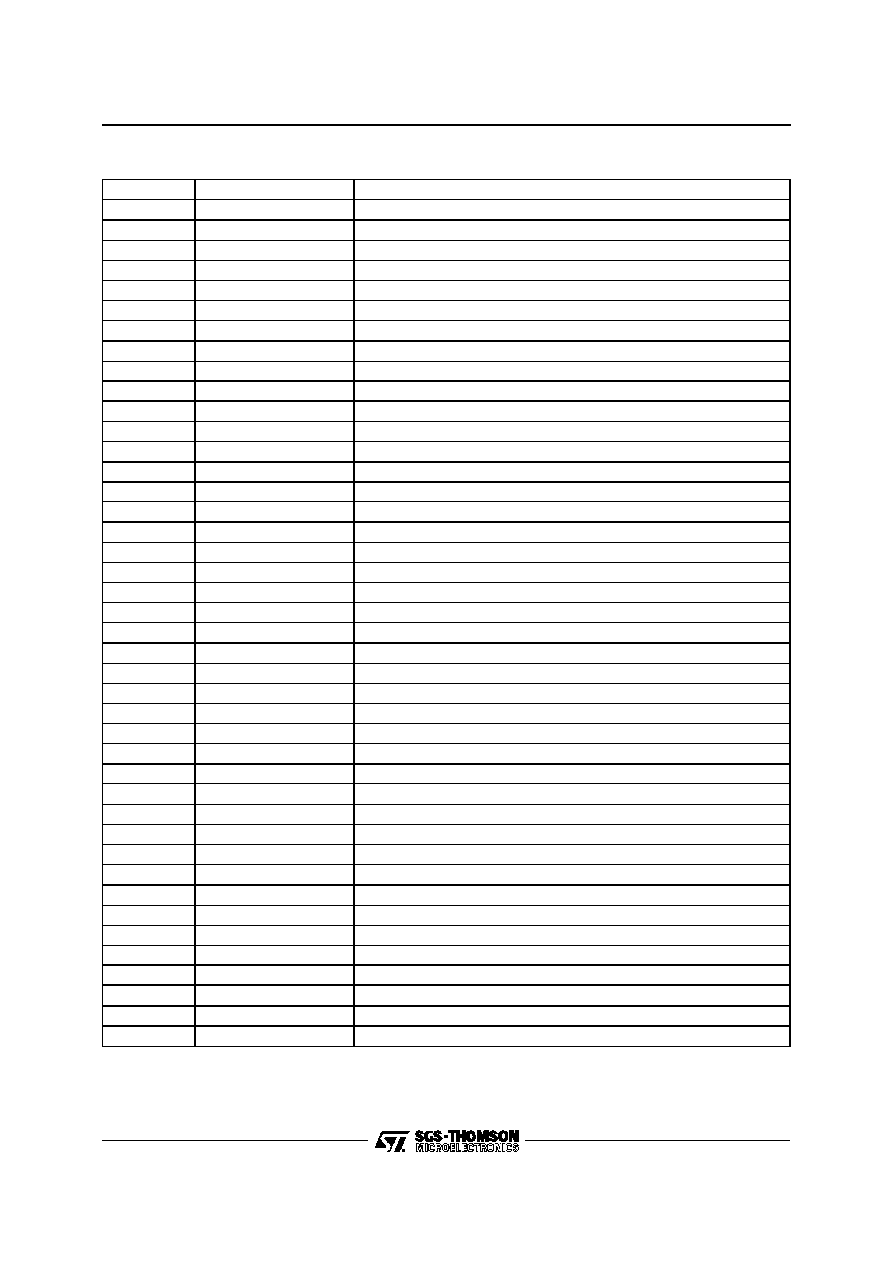
Pin Number
Name
Function
1
FC R
Audio Roll-off Right
3
SUM OUT
Noise Reduction Summing Output
2
PK IN
Noise Reduction Peak Detector Input
4
VOL R
Volume Controlled Audio Out Right
5
S1 VID OUT
TV-Scart 1 Video Output
6
S2 VID OUT
VCR-Scart 2 Video Output
7
VOL L
Volume Controlled Audio Out Left
8
S2 VID RTN
VCR-Scart 2 Video Return
9
S2 OUT L
Fixed Level Audio Output Left
10
CLAMP IN
Sync-Tip Clamp Input
11
S2 OUT R
Fixed Level Audio Output Right
12
UNCL DEEM
Unclamped Deemphasized Video Output
13
VIDEEM2/22kHz
Video Deemphasis 2 or 22kHz Output
14
V 12V
Video 12V Supply
15
VIDEEM1
Video Deemphasis 1
16
V GND
Video Ground
17
B-BAND IN
Base Band Input
18
S2 RTN L
Auxiliary Audio Return Left
19
S2 RTN R
Auxiliary Audio Return Right
20
FM IN
FM Demodulator Input
21
AGC L
AGC Peak Detector Capacitor Left
22
SCL
I
2
C Bus Clock
23
SDA
I
2
C Bus Data
24
XTL
4/8MHz Quartz Crystal or Clock Input
25
V
DD
5V
Digital 5V Power Supply
26
GND 5V
Digital Power Ground
27
CPUMP L
FM PLL Charge Pump Capacitor Left
28
DET L
FM PLL Filter Left
29
U75 L
Deemphasis Time Constant Left
30
AMPLK L
Amplitude Detector Capacitor Left
31
AGC R
AGC Peak Detector Capacitor Right
32
A GND L
Audio Ground
33
V
REF
2.4V Reference
34
A 12V
Audio 12V Supply
35
AMPLK R
Amplitude Detector Capacitor Left
36
DET R
FM PLL Filter Right
37
U75 R
Deemphasis Time Constant Right
38
CPUMP R
FM PLL Charge Pump Capacitor Right
39
I
REF
Current Reference Resistor
40
PK OUT
Noise Reduction Peak Detector Output
41
FC L
Audio Roll-off Left
42
A GND R
Audio Ground
00
42
A
-
01.
T
B
L
STV0042A
2/24

PIN DESCRIPTION
1 - Sound Detection
FMIN
This is the input to the two FM demodulators. It
feeds two AGC amplifiers with a bandwidth of at
least 5-10MHz. There is one amplifier for each
channel both with the same input. The AGC ampli-
fiers have a 0dB to +40dB range.
Z
IN
= 5k
, Min input = 2mV
PP
per subcarrier.
Max input = 500mV
PP
(max when all inputs are
added together, when their phases coincide).
AGC L, AGC R
AGC amplifiers peak detector capacitor connec-
tions. The output current has an attack/decayratio
of 1:32. That is the ramp up current is approxi-
mately 5
µ
A and decay current is approximately
160
µ
A. 11V gives maximum gain. These pins are
also driven by a circuit monitoring the voltage on
AMPLK L and AMPLK R respectively.
AMPLK L, AMPLK R
The outputs of amplitude detectors LEFT and
RIGHT. Each requires a capacitor and a resistor to
GND. The voltage across this is used to decide
whether there is a signal being received by the FM
detector. The level detector output drives a bit in
the detector I
2
C bus control block.
AMPLK L and AMPLK R drive also respectively
AGC L and AGC R. For instance when the voltage
on AMPLK L is > (V
REF
+ 1 V
BE
) it sinks current to
V
REF
from pin AGCL to reduce the AGC gain.
DET L, DET R
Respectively the outputs of the FM phase detector
left and right. This is for the connection of an
external loop filter for the PLL. The output is a
push-pull current source.
CPUMP L, CPUMP R
The output from the frequency synthesizer is a
push-pullcurrent source which requiresa capacitor
to ground to derive a voltage to pull the VCO to the
target frequency. The output is
±
100
µ
A to achieve
lockand
±
2
µ
A during lock to provide a trackingtime
constant of approximately 10Hz.
VREF
This is the audio processor voltage reference used
through out the FM/audio section of the chip. As
such it is essential that it is well decoupled to
ground to reduce as far as possible the risk of
crosstalk and noise injection. This voltage is de-
rived directly from the bandgap reference of 2.4V.
The V
REF
output can sink up to 500
µ
A in normal
operation and 100
µ
A when in stand-by.
IREF
This is a bufferedV
REF
outputto an off-chip resistor
to produce an accurate current reference, within
the chip, for the biasing of amplifiers with current
outputs into filters. It is also required for the Noise
reduction circuit to provide accurate roll-off fre-
quencies.
This pin should not be decoupled as it would inject
current noise. The target current is 50
µ
A
±
2% thus
a 47.5k
±
1% is required.
A 12V
Double bonded main power pin for the audio/FM
section of the chip. The two bond connections are
to the ESD and to power the circuit and on chip
regulators/references.
A GND L
This ground pin is double bonded :
1) to channel LEFT : RF section & VCO,
2) to both AGC amplifiers, channel LEFT and
RIGHT audio filter section.
A GND R
This ground pin is double bonded :
1) to the volume control, noise reduction system,
ESD + Mux + V
REF
2) to channel right : RF section & VCO
2 - Baseband Audio Processing
PK OUT
The noise reduction control loop peak detector
output requires a capacitor to ground from this pin,
and a resistor to V
REF
pin to give some accurate
decaytime constant.An on chip5k
±
25 % resistor
and external capacitor give the attack time.
PK IN
This pin is an input to a control loop peak detector
and is connectedto the output of the offchip control
loop band pass filter.
SUM OUT
The two audio demodulated signals are summed
together by means of an amplifier with a gain of 0.5.
If both inputs are 1V then the output is 1V. This
amplifier has an input follower buffer which gives a
V
BE
offset in the DC bias voltage. Thus the filter
which this amplifier drives must include AC cou-
pling to the next stage (PK IN Pin).
FC L, FC R
The variable bandwidth transconductance ampli-
fier has a current output which is variable depend-
ing on the input signal amplitude as defined by the
control loop of the noise reduction. The output
current is then dumped into an off-chip capacitor
which together with the accurate current reference
define the min/max rolloff frequencies.A resistor in
series with a capacitor is connected to ground from
these two pins.
STV0042A
3/24

U75 L, U75 R
External deemphasis networks for channels left and
right. For each channel a capacitor and resistor in
parallel of 75
µ
s time constant are connectedbetween
hereandV
REF
to provide 75
µ
s de-emphasis.Internally
selectable is an internal resistor that can be pro-
grammedtobe addedin paralleltherebyconvertingthe
networkto approx50
µ
s de-emphasis(see controlblock
map).The value of theinternal resistors is 30k
±
30%.
Theamplifier forthisfilterisvoltageinput,currentoutput;
with
±
500mV input the outputwill be
±
55
µ
A.
VOL L, VOL R
Themainaudiooutputfrom thevolumecontrolamplifier
the signal to get output signals as high as 2V
RMS
(+12dB) on a DC bias of 4.8V.Control is from +12dBto
-26.75dB plus Mute with 1.25dB steps. This amplifier
has short circuit protection and is intended to drive a
SCART connector directly via AC coupling and meets
thestandardSCARTdriverequirements.Theseoutputs
featurehigh impedancemode for parallel connection.
S2 OUT L, S2 OUT R
These audio outputs are sourced directly from the
audioMUX, andas a result do not includeany volume
controlfunction.Theywill outputa1V
RMS
signalbiased
at4.8V.They are shortcircuit protected.Theseoutputs
feature high impedance mode for parallel connection
and meetSCART drive requirement.
S2 RTN L, S2 RTN R
These pins allow auxiliary audio signals to be con-
nected to the audio processor and hence makes
use of the on-chip volume control. For additional
details please refer to the audio switching table.
3 - Video Processing
B-BAND IN
AC-coupled video input from a tuner.
Z
IN
> 10k
±
25%. This drives an on-chipvideo ampli-
fier.TheotherinputofthisampisACgroundedbybeing
connectedto an internal V
REF
. The videoamplifier has
selectablegain from 0dBto 12.7dBin 63 stepsand its
output signal can be selected normal or inverted.
UNCL DEEM
Deemphasized still unclamped output. It is also an
input of the video matrix.
VIDEEM1
Connected to an external de-emphasis network
(for instance 625 lines PAL de-emphasis).
VIDEEM2 / 22kHz
Connected to an external de-emphasis network
(for instance 525 lines NTSC or other video de-em-
phasis). Alternatively a precise 22kHz tone may be
output by I
2
C bus control.
CLAMP IN
This pin clampsthemost negativeextremeof theinput
(the sync tips) to 2.7V
DC
(or appropriatevoltage). The
video at the clamp input is only 1V
PP
. This clamped
video which is de-emphasised, filtered and clamped
(energydispersalremoved) is normal, negativesyncs,
video. This signal drives the Video Matrix input called
Normal Video. It has a weak (1.0
µ
A
±
15 %) stable
current source pulling the input towards GND. Other-
wise the input impedance is very high at DC to 1kHz
Z
IN
> 2M
. Video bandwidth through this is -1dB at
5.5MHz. The CLAMP input DC restore voltageis then
usedas a means for gettingthecorrect DC voltageon
the SCART outputs.
S2 VID RTN
External video input 1.0V
PP
AC coupled 75
source impedance. This input has a DC restoration
clamp on its input. The clamp sink current is 1
µ
A
±
15% with the buffer Z
IN
> 1M
. This signal is an
input to the Video Matrix.
S1 VID OUT, S2 VID OUT
Videodrivers for SCART 1 and SCART 2. An external
emitter follower bufferis required to drive a 150
load.
The average DC voltage to be 1.5V on the O/P. The
signalis video2.0V
PP
5.5MHzBW with synctip = 1.2V.
These pins get signals from the Video Matrix. The
signalselected from theVideo Matrix for outputon this
pin is controlled by a control register. This output also
featureahighimpedancemodeforparallelconnection.
V 12V
+12V double bonded : ESD+guard rings and video
circuit power.
V GND
Doubled bonded. Clean VID IN GND. Strategically
placed video power ground connection to reduce
video currents getting into the rest of the circuit.
4 - Control Block
GND 5V
The main power ground connection for the control
logic, registers, the I
2
C bus interface, synthesizer
& watchdog and XTLOSC.
VDD 5V
Digital +5V power supply.
SCL
This is the I
2
C busclock line. Clock = DC to 100kHz.
Requires external pull up eg. 10k
to 5V.
SDA
This is the I
2
C bus data line. Requires external pull
up eg. 10k
to 5V.
XTL
This pin allows for the on-chip oscillator to be either
used with a crystal to ground of 4MHz or 8MHz, or
to be driven by an external clock source. The
external source can be either 4MHz or 8MHz. A
programmablebit in the control block removes a
˜
2
block when the 4MHz option is selected.
PIN DESCRIPTION (continued)
STV0042A
4/24
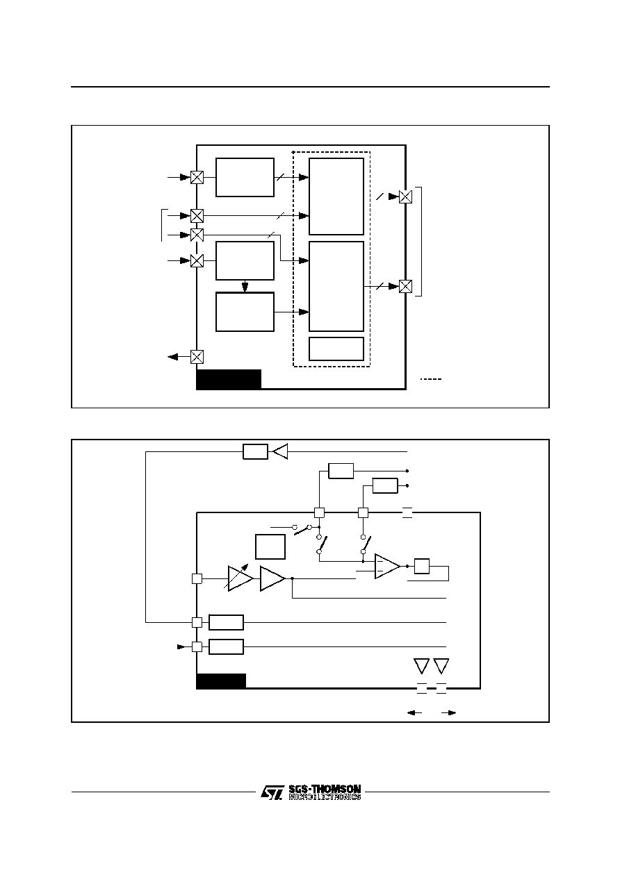
STV0042A
B-BAND
Video
Processing
4 x 2
Video
Matrix
2
2
From Tuner
Audio
Matrix
+
Volume
FM
Demodulation
2 Channels
From Tuner
Noise
Reduction +
Deemphasis
1
I
2
C Bus
Interface
From
VCR/Decoder
22kHz to LNB
2
2
To TV, VCR/Decoder
Active in Stand-by
00
42
A
-
0
2
.
E
P
S
GENERAL BLOCK DIAGRAM
CLAMP
CLAMP
Normal
VCR / Decoder Return
To Decoder or VCR
To TV
S1 VID OUT
S2 VID OUT
S2 VID RTN
CLAMP IN
G
B-BAND IN
STV0042A
22kHz
TONE
Baseband
LPF
VIDEEM1
VIDEEM2/22kHz
UNCL DEEM
NTSC
PAL
Deemphasized
±
1
17
13
15
12
5
6
8
10
˜
2
00
42
A
-
03.
E
P
S
VIDEO PROCESSING BLOCK DIAGRAM
STV0042A
5/24