 | –≠–ª–µ–∫—Ç—Ä–æ–Ω–Ω—ã–π –∫–æ–º–ø–æ–Ω–µ–Ω—Ç: STV0042Z | –°–∫–∞—á–∞—Ç—å:  PDF PDF  ZIP ZIP |
STV0042A/Z
Analog Satellite Sound and Video Processor
Æ
September 2003
1/37
Sound Features
s
Two Independent Sound Demodulators
s
PLL Demodulation with 5-10 MHz Frequency
Synthesis
s
Programmable FM Demodulator Bandwidth
accommodating FM Deviations between ±30
and ±400 kHz
s
Programmable 50/75 µs or No De-emphasis
s
Dynamic Noise Reduction (ANRS)
s
One or Two Auxiliary Audio Inputs and
Outputs
s
Gain-controlled and Mutable Audio Outputs
s
High-impedance Mode Audio Outputs for
Twin Tuner Applications
Video Features
s
Composite 6-bit Video with 0 to 12.7 dB Gain
Control
s
Selectable Composite Video Inverter
s
Two Selectable Video De-emphasis Networks
s
4 x 2 Video Matrix
s
High-impedance Mode Video Outputs for
Twin Tuner Applications
Miscellaneous Features
s
22 kHz Tone Generation for LNB Control
s
I≤C Bus Control: Chip Addresses = 06h
s
Low Power Stand-by Mode with Active Audio
and Video Matrices
General Description
The STV0042 BICMOS integrated circuit is
designed for low-cost analog satellite receiver
applications.
The STV0042A/Z performs all the necessary signal
processing from the tuner to the Audio/Video input
and output connectors regardless of the satellite
system.
SHRINK42
(Shrink Plastic Dual In-Line Package)
ORDER CODE: STV0042A/Z

STV0042A/Z
2/37
Table of Contents
Chapter 1
General Information . . . . . . . . . . . . . . . . . . . . . . . . . . . . . . . . . . . . . . . . . . . . . . . .3
1.1
Pin Description .................................................................................................................. 3
Chapter 2
Circuit Description . . . . . . . . . . . . . . . . . . . . . . . . . . . . . . . . . . . . . . . . . . . . . . . .13
Chapter 3
Input/Output Diagrams . . . . . . . . . . . . . . . . . . . . . . . . . . . . . . . . . . . . . . . . . . . .15
Chapter 4
I≤C Protocol . . . . . . . . . . . . . . . . . . . . . . . . . . . . . . . . . . . . . . . . . . . . . . . . . . . . . .19
4.1
Writing to the Chip .............................................................................................................. 19
4.2
Reading from the Chip ....................................................................................................... 19
Chapter 5
Control Registers . . . . . . . . . . . . . . . . . . . . . . . . . . . . . . . . . . . . . . . . . . . . . . . . .20
Chapter 6
FM Demodulation Software Routine . . . . . . . . . . . . . . . . . . . . . . . . . . . . . . . . . .25
6.1
Detailed Description ........................................................................................................... 25
Chapter 7
Application Diagrams . . . . . . . . . . . . . . . . . . . . . . . . . . . . . . . . . . . . . . . . . . . .28
Chapter 8
Electrical Characteristics . . . . . . . . . . . . . . . . . . . . . . . . . . . . . . . . . . . . . . . . . .30
8.1
Absolute Maximum Ratings .............................................................................................. 30
8.2
Thermal Data .................................................................................................................... 30
8.3
Electrical Characteristics .................................................................................................... 30
Chapter 9
Package Mechanical Data . . . . . . . . . . . . . . . . . . . . . . . . . . . . . . . . . . . . . . . . .35
Chapter 10
Revision History . . . . . . . . . . . . . . . . . . . . . . . . . . . . . . . . . . . . . . . . . . . . . . . . . .36
3/37
STV0042A/Z
General Information
1
General Information
1.1
Pin Description
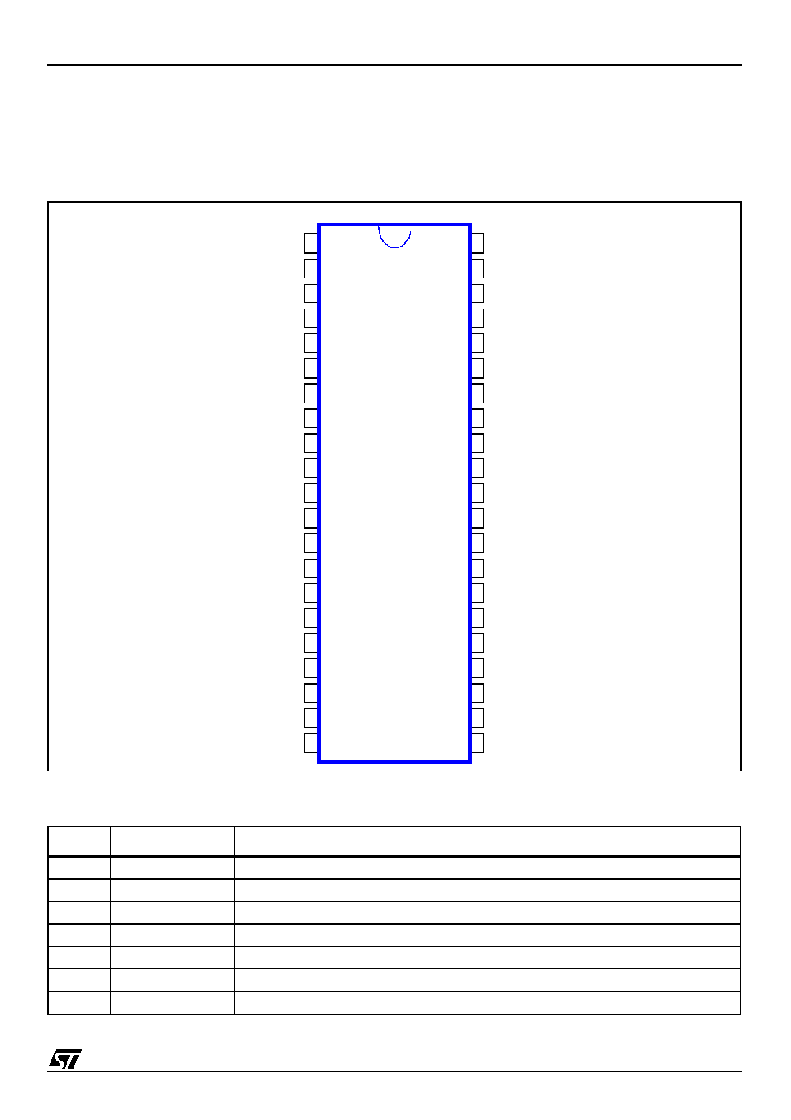
Figure 1: Pin Connections
Table 1: Pin Description (Sheet 1 of 2)
Pin No.
Name
Function
1
FCR
Audio Roll-off Right
2
PKIN
Noise Reduction Peak Detector Input
3
SUMOUT
Noise Reduction Summing Output
4
VOLR
Right Volume-controlled Audio Output
5
S1VIDOUT
TV SCART Video Output 1
6
S2VIDOUT
VCR SCART Video Output 2
7
VOLL
Left Volume-controlled Audio Output
AGNDR
FCL
PKOUT
IREF
CPUMPR
U75R
DETR
AMPLKR
A12V
VREF
AGNDL
AGCR
AMPLKL
U75L
DETL
CPUMPL
GND5V
VDD5V
XTL
SDA
SCL
1
2
3
4
5
6
7
8
9
10
11
12
13
14
15
16
17
18
19
20
21
42
41
40
39
38
37
36
35
34
33
32
31
30
29
28
27
26
25
24
23
22
FCR
PKIN
SUMOUT
VOLR
S1VIDOUT
S2VIDOUT
VOLL
S2VIDRTN
S2OUTL
CLAMPIN
S2OUTR
UNCLDEEM
VIDEEM2/22KHZ
V12V
VIDEEM1
VGND
BBANDIN
S2RTNL
S2RTNR
FMIN
AGCL
General Information
STV0042A/Z
4/37
8
S2VIDRTN
VCR SCART Video Return 2
9
S2OUTL
Left Fixed Level Audio Output
10
CLAMPIN
Sync Tip Clamp Input
11
S2OUTR
Right Fixed Level Audio Output
12
UNCLDEEM
Unclamped De-emphasized Video Output
13
VIDEEM2/22KHZ
Video De-emphasis 2 or 22 kHz Output
14
V12V
12 V Video Power Supply
15
VIDEEM1
Video De-emphasis 1
16
VGND
Video Ground
17
BBANDIN
Base Band Input
18
S2RTNL
Left Auxiliary Audio Return
19
S2RTNR
Right Auxiliary Audio Return
20
FMIN
FM Demodulator Input
21
AGCL
Left AGC Peak Detector Capacitor
22
SCL
I≤C Bus Clock
23
SDA
I≤C Bus Data
24
XTL
4/8 MHz Crystal Oscillator or Clock Input
25
VDD5V
Digital 5 V Power Supply
26
GND5V
Digital Ground
27
CPUMPL
Left FM PLL Charge Pump Capacitor
28
DETL
Left FM PLL Filter
29
U75L
Left De-emphasis Time Constant
30
AMPLKL
Left Amplitude Detector Capacitor
31
AGCR
Right AGC Peak Detector Capacitor
32
AGNDL
Left Audio Ground
33
VREF
2.4 V Reference Power Supply
34
A12V
12 V Audio Power Supply
35
AMPLKR
Right Amplitude Detector Capacitor
36
DETR
Right FM PLL Filter
37
U75R
Right De-emphasis Time Constant
38
CPUMPR
Right FM PLL Charge Pump Capacitor
39
IREF
Current Reference Resistor
40
PKOUT
Noise Reduction Peak Detector Output
41
FCL
Left Audio Roll-off
42
AGNDR
Right Audio Ground
Table 1: Pin Description (Sheet 2 of 2)
Pin No.
Name
Function
5/37
STV0042A/Z
General Information
1.1.1
Sound Detection
1.1.1.1 FM Demodulators
A block diagram of the FM Demodulation block is shown in
Figure 3
.
Pin FMIN (pin 20) is the input to the two FM demodulators. It feeds two AGC amplifiers with a
bandwidth of at least 5 to 10 MHz. There is one amplifier for each channel. Both channels have the
same input. The AGC amplifiers have a range between 0 and +40 dB.
The input impedance (Z
IN
) is 5 k
with a minimum input of 2 mV
PP
per subcarrier and a maximum
input of 500 mV
PP
. This is the maximum value when all inputs are added together, when their
phases coincide.
1.1.1.2 AGC Peak Detector Capacitors
Pins AGCL and AGCR (pins 21 and 31, respectively) are the AGC amplifier peak detector capacitor
connections. The output current has an attack/decay ratio of 1:32. This means that the ramp-up
current is approximately 5 µA and decay current is approximately 160 µA. 11V gives maximum
gain. These pins are also driven by a circuit monitoring the voltage on pins AMPLKL and AMPLKR,
respectively.
1.1.1.3 Amplitude Detector Capacitors
Pins AMPLKL and AMPLKR (pins 30 and 35, respectively) are the left and right outputs of their
respective amplitude detectors. Each pin requires a capacitor and a resistor to GND. The voltage
across these pins is used to decide whether a signal is being received by the FM detector. The level
detector output drives a bit in the I≤C bus detector control block. Pins AMPLKL and AMPLKR drive
also respectively pins AGCL and AGCR. For instance, when the voltage on pin AMPLKL is > (V
REF
+ 1 V
BE
) it sinks current to V
REF
from pin AGCL in order to reduce the AGC gain.
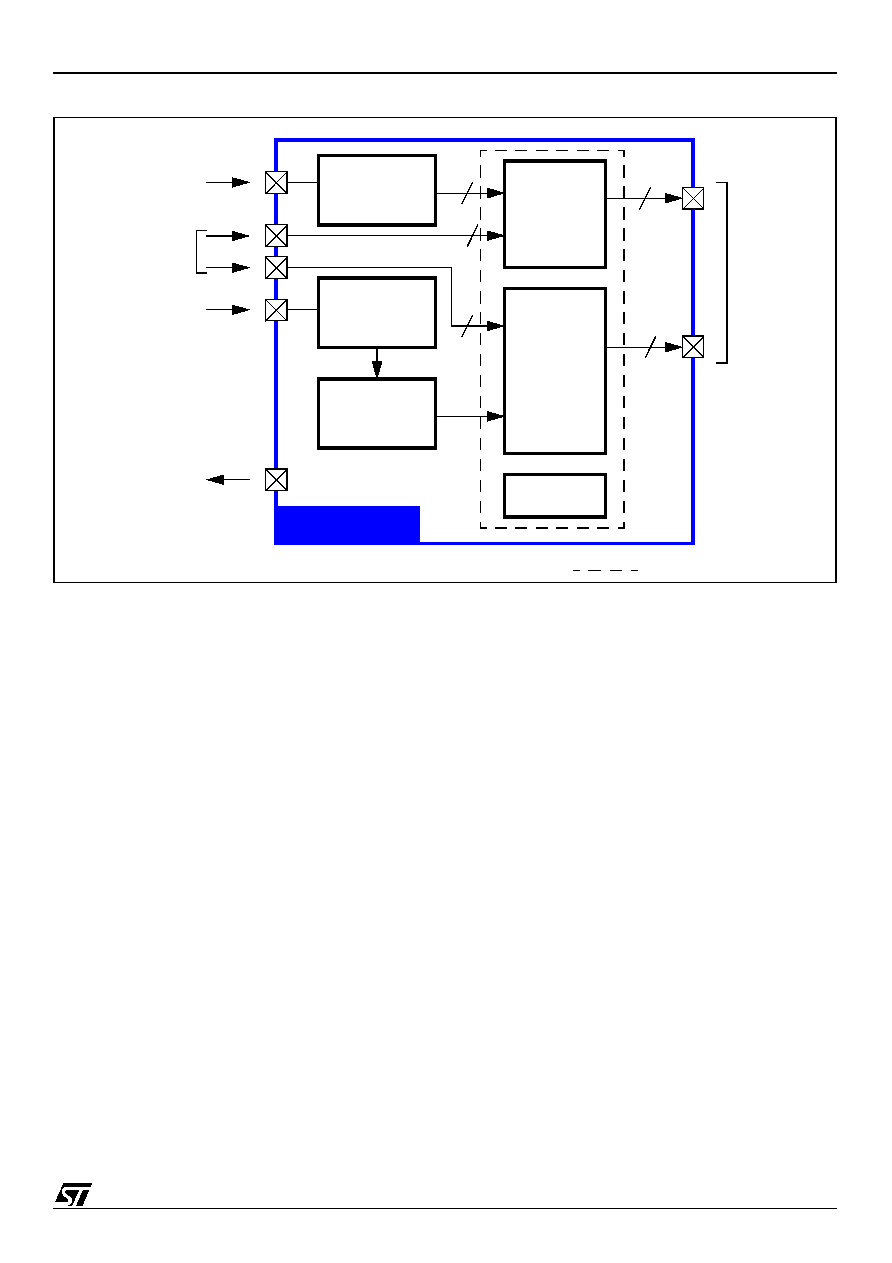
Figure 2: STV0042A/Z General Block Diagram
STV0042A/Z
From Tuner
From Tuner
From
VCR/Decoder
22 kHz to LNB
B-Band
Video
Processing
FM
Demodulation
2 Channels
Noise
Reduction
& De-emphasis
4 x 2
Video
Matrix
Audio
Matrix
&
Volume
I≤C Bus
Interface
To
TV
VCR
Decoder
2
2
Active in Standby mode
2
2
1