 | –≠–ª–µ–∫—Ç—Ä–æ–Ω–Ω—ã–π –∫–æ–º–ø–æ–Ω–µ–Ω—Ç: STV0056 | –°–∫–∞—á–∞—Ç—å:  PDF PDF  ZIP ZIP |
STV0056A
SATELLITE SOUND AND VIDEO PROCESSOR
September 1996
ADVANCE DATA
SOUND
.
TWO INDEPENDENT SOUND DEMODULA-
TORS
.
PLL DEMODULATION WITH 5-10MHz FRE-
QUENCY SYNTHESIS
.
PROGRAMMABLE
FM
DEMODULATOR
BANDWIDTH ACCOMODATING FM DEVIA-
TIONS FROM
±
30kHz TILL
±
400kHz
.
PROGRAMMABLE 50/75
µ
s, J17 OR NO DE-
EMPHASIS
.
WEGENER PANDA SYSTEM
.
TWO AUXILIARY AUDIO INPUTS AND OUT-
PUTS
.
GAIN
CONTROLLED
AND
MUTEABLE
AUDIO OUTPUTS
.
HIGH IMPEDANCE MODE AUDIO OUTPUTS
FOR TWIN TUNER APPLICATIONS
VIDEO
.
COMPOSITE VIDEO 6-bit 0 to 12.7dB GAIN
CONTROL
.
COMPOSITE
VIDEO
SELECTABLE
IN-
VERTER
.
TWO SELECTABLE VIDEO DE-EMPHASIS
NETWORKS
.
6 x 3 VIDEO MATRIX
.
BLACK LEVEL ADJUSTABLE OUTPUT FOR
ON-BOARD VIDEOCRYPT DECODER
.
HIGH IMPEDANCE MODE VIDEO OUTPUTS
FOR TWIN TUNER APPLICATIONS
MISCELLANEOUS
.
22kHz TONE GENERATION FOR LNB CON-
TROL
.
I
2
C BUS CONTROL
CHIP ADDRESSES = 06
HEX
OR 46
HEX
.
LOW POWER STAND-BY MODE WITH AC-
TIVE AUDIO AND VIDEO MATRIXES
DESCRIPTION
The STV0056A BICMOS integrated circuit realizes
all the necessary signal processing from the tuner
to the Audio/Video input and output connectors
regardless the satellite system.
This is advance information on a new product now in development or undergoing evaluation. Details are subject to change without no tice.
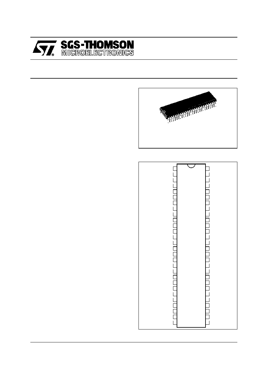
SHRINK56
(Plastic Package)
ORDER CODE : STV0056A
1
2
3
4
5
6
7
8
9
10
11
12
13
14
15
16
17
18
19
20
21
22
23
24
25
26
27
28
48
47
46
45
44
43
42
41
40
39
38
37
36
35
34
33
32
31
30
29
49
50
51
52
53
54
55
56
FC R
PK IN R
LEVEL R
S1 VID RTN
S3 VID RTN
VOL R
S3 VID OUT
S1 VID OUT
S2 VID OUT
VOL L
S2 VID RTN
S2 OUT L
CLAMP IN
S2 OUT R
UNCL DEEM
VIDEEM2/22kHz
V 12V
VIDEEM1
B-BAND IN
V GND
S2 RTN L
S2 RTN R
FM IN
S3 RTN L
S3 RTN R
S3 OUT L
S3 OUT R
AGC L
A GND R
FC L
PK IN L
LEVEL L
PK OUT L
PK OUT R
I
REF
CPUMP R
U75 R
DET R
AMPLK R
A 12V
V
REF
A GND L
AGC R
AMPLK L
U75 L
DET L
CPUMP L
GND 5V
V
DD
5V
XTL
HA
J17 R
J17 L
SDA
SCL
I/O/22kHz
0056A-01.EPS
PIN CONNECTIONS
1/26
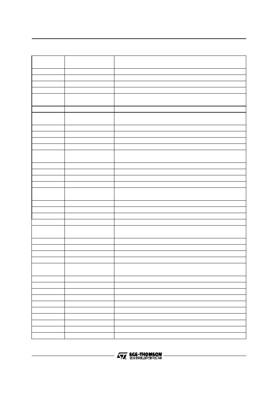
PIN ASSIGNMENT
Pin Number
Name
Function
1
FC R
Audio Roll-off Right
2
PK IN R
Noise Reduction Peak Detector Input Right
3
LEVEL R
Noise Reduction Level Right
4
S1 VID RTN
TV-Scart 1 Video Return
5
S3 VID RTN
Decoder-Scart Video Return
6
VOL R
Volume Controlled Audio Out Right
7
S3 VID OUT
Decoder-Scart Video Output
8
S1 VID OUT
TV-Scart 1 Video Output
9
S2 VID OUT
VCR-Scart 2 Video Output
10
VOL L
Volume Controlled Audio Out Left
11
S2 VID RTN
VCR-Scart 2 Video Return
12
S2 OUT L
Fixed Level Audio Output Left (to VCR)
13
CLAMP IN
Sync-Tip Clamp Input
14
S2 OUT R
Fixed Level Audio Output Right (to VCR)
15
UNCL DEEM
Unclamped Deemphasized Video Output
16
VIDEEM2/22kHz
Video Deemphasis 2 or 22kHz Output
17
V 12V
Video 12V Supply
18
VIDEEM1
Video Deemphasis 1
19
V GND
Video Ground
20
B-BAND IN
Base Band Input
21
S2 RTN L
Auxiliary Audio Return Left (from VCR)
22
S2 RTN R
Auxiliary Audio Return Right (from VCR)
23
FM IN
FM Demodulator Input
24
S3 RTN L
Auxiliary Audio Return Left (from decoder)
25
S3 RTN R
Auxiliary Audio Return Right (from decoder)
26
AGC L
AGC Peak Detector Capacitor Left
27
S3 OUT L
Auxiliary Audio Output L (to decoder)
28
S3 OUT R
Auxiliary Audio Output R (to decoder)
29
I/O/22kHz
Digital Input/Output or 22kHz Output
30
SCL
I
2
C Bus Clock
31
SDA
I
2
C Bus Data
32
HA
Hardware Address
33
J17 R
J17 Deemphasis Time Constant Right
34
J17 L
J17 Deemphasis Time Constant Left
35
XTL
4/8MHz Quartz Crystal or Clock Input
36
V
DD
5V
Digital 5V Power Supply
37
GND 5V
Digital Power Ground
38
CPUMP L
FM PLL Charge Pump Capacitor Left
39
DET L
FM PLL Filter Left
40
U75 L
Deemphasis Time Constant Left
41
AMPLK L
Amplitude Detector Capacitor Left
42
AGC R
AGC Peak Detector Capacitor Right
43
A GND L
Audio Ground
44
V
REF
2.4V Reference
0056A-01.TBL
STV0056A
2/26
Pin Number
Name
Function
45
A 12V
Audio 12V Supply
46
AMPLK R
Amplitude Detector Capacitor Left
47
DET R
FM PLL Filter Right
48
U75 R
Deemphasis Time Constant Right
49
CPUMP R
FM PLL Charge Pump Capacitor Right
50
I
REF
Current Reference Resistor
51
PK OUT R
Noise Reduction Peak Detector Output Right
52
PK OUT L
Noise Reduction Peak Detector Output Left
53
LEVEL L
Noise Reduction Level Left
54
PK IN L
Noise Reduction Peak Detector Input
55
FC L
Audio Roll-off Left
56
A GND R
Audio Ground
0056A-01.TBL
PIN ASSIGNMENT (continued)
SOUND DETECTION
FMIN
This is the input to the two FM demodulators. It
feeds two AGC amplifiers with a bandwidth of at
least 5-10MHz. There is one amplifier for each
channel both with the same input. The AGC ampli-
fiers have a 0dB to +40dB range.
Z
IN
= 5k
, Min input = 2mV
PP
per subcarrier.
Max input = 500mV
PP
(max when all inputs are
added together, when their phases coincide).
AGC L, AGC R
AGC amplifiers peak detector capacitor connec-
tions. The output current has an attack/decay ratio
of 1:32. That is the ramp up current is approxi-
mately 5
µ
A and decay current is approximately
160
µ
A. 11V gives maximum gain. These pins are
also driven by a circuit monitoring the voltage on
AMPLK L and AMPLK R respectively.
AMPLK L, AMPLK R
The outputs of amplitude detectors LEFT and
RIGHT. Each requires a capacitor and a resistor to
GND. The voltage across this is used to decide
whether there is a signal being received by the FM
detector. The level detector output drives a bit in
the detector I
2
C bus control block.
AMPLK L and AMPLK R drive also respectively
AGC L and AGC R. For instance when the voltage
on AMPLK L is > (V
REF
+ 1 V
BE
) it sinks current to
V
REF
from pin AGCL to reduce the AGC gain.
DET L, DET R
Respectively the outputs of the FM phase detector
left and right.
This is for the connection of an external loop filter
for the PLL. The output is a push-pull current
source.
CPUMP L, CPUMP R
The output from the frequency synthesizer is a
push-pull current source which requires a capacitor
to ground to derive a voltage to pull the VCO to the
target frequency. The output is
±
100
µ
A to achieve
lock and
±
2
µ
A during lock to provide a tracking time
constant of approximately 10Hz.
V
REF
This is the audio processor voltage reference used
through out the FM/audio section of the chip. As
such it is essential that it is well decoupled to
ground to reduce as far as possible the risk of
crosstalk and noise injection. This voltage is de-
rived directly from the bandgap reference of 2.4V.
The V
REF
output can sink up to 500
µ
A in normal
operation and 100
µ
A when in stand-by.
I
REF
This is a buffered V
REF
output to an off-chip resistor
to produce an accurate current reference, within
the chip, for the biasing of amplifiers with current
outputs into filters. It is also required for the Noise
reduction circuit to provide accurate roll-off fre-
quencies. This pin should not be decoupled as it
would inject current noise. The target current is
50
µ
A
±
2% thus a 47.5k
±
1% is required.
PIN DESCRIPTION
STV0056A
3/26

A 12V
Double bonded main power pin for the audio/FM
section of the chip. The two bond connections are
to the ESD and to power the circuit and on chip
regulators/references.
A GND L
This ground pin is double bonded :
1) to channel LEFT : RF section & VCO,
2) to both AGC amplifiers, channel LEFT and
RIGHT audio filter section.
A GND R
This ground pin is double bonded :
1) to the volume control, noise reduction system,
ESD + Mux + V
REF
2) to channel right : RF section & VCO
BASEBAND AUDIO PROCESSING
PK OUT L, PK OUT R, PK OUT
The noise reduction control loop peak detector
output requires a capacitor to ground from this pin,
and a resistor to V
REF
pin to give some accurate
decay time constant. An on chip 5k
±
25 % resistor
and external capacitor give the attack time.
PK IN L, PK IN R or PK IN
Each of these pins is an input to a control loop peak
detector and is connected to the output of the
offchip control loop band pass filter.
LEVEL L, LEVEL R
Respectively the audio left and right signals of the
FM demodulators are output to level L and level R
pins through an input follower buffer. The off-chip
filters driven by these pins must include AC cou-
pling to the next stage (PK IN L and PK IN R pins
respectively).
FC L, FC R
The variable bandwidth transconductance ampli-
fier has a current output which is variable depend-
ing on the input signal amplitude as defined by the
control loop of the noise reduction. The output
current is then dumped into an off-chip capacitor
which together with the accurate current reference
define the min/max rolloff frequencies. Aresistor in
series with a capacitor is connected to ground from
these two pins.
J17 L, J17 R
The external J17 de-emphasis networks for chan-
nels left and right. The amplifier for this filter is
voltage input, current output. Output with
±
500mV
input will be
±
55
µ
A.
To perform J17 de-emphasis with the STV0042, an
external circuit is required.
U75 L, U75 R
External deemphasis networks for channels left
and right. For each channel a capacitor and resistor
in parallel of 75
µ
s time constant are connected
between here and V
REF
to provide 75
µ
s de-empha-
sis. Internally selectable is an internal resistor that
can be programmed to be added in parallel thereby
converting the network to approx 50
µ
s de-empha-
sis (see control block map). The value of the inter-
nal resistors is 54k
±
30 %. The amplifier for this
filter is voltage input, current output ; with
±
500mV
input the output will be
±
55
µ
A.
VOL L, VOL R
The main audio output from the volume control
amplifier the signal to get output signals as high as
2V
RMS
(+12dB) on a DC bias of 4.8V. Control is
from +12dB to -26.75dB plus Mute with 1.25dB
steps. This amplifier has short circuit protection and
is intended to drive a SCART connector directly via
AC coupling and meets the standard SCART drive
requirements. These outputs feature high imped-
ance mode for parallel connection.
S2 OUT L, S2 OUT R, S3 OUT L, S3 OUT R
These audio outputs are sourced directly from the
audio MUX, and as a result do not include any
volume control function. They will output a 1V
RMS
signal biased at 4.8V. They are short circuit pro-
tected. These outpu ts feature high impedance
mode for parallel connection and meet SCART
drive requirement.
S2 RTN L, S2 RTN R, S3 RTN L, S3 RTN R
These pins allow auxiliary audio signals to be con-
nected to the audio processor and hence makes
use of the on-chip volume control. For additional
details please refer to the audio switching table.
PIN DESCRIPTION (continued)
STV0056A
4/26

VIDEO PROCESSING
B-BAND IN
AC-coupled video input from a tuner.
Z
IN
> 10k
±
25%. This drives an on-chip video
amplifier. The other input of this amp is AC
grounded by being connected to an internal V
REF
.
The video amplifier has selectable gain from 0dB
to 12.7dB in 63 steps and its output signal can be
selected normal or inverted.
UNCL DEEM
Deemphasized still unclamped output. It is also an
input of the video matrix.
VIDEEM1
Connected to an external de-emphasis network
(for instance 625 lines PAL de-emphasis).
VIDEEM2 / 22kHz
Connected to an external de-emphasis network
(for instance 525 lines NTSC or other video de-em-
phasis). Alternatively a precise 22kHz tone may be
output by I
2
C bus control.
CLAMP IN
This pin clamps the most negative extreme of the
input (the sync tips) to 2.7V
DC
(or appropriate volt-
age). The video at the clamp input is only 1V
PP
.
This clamped video which is de-emphasised, fil-
tered and clamped (energy dispersal removed) is
normal, negative syncs, video. This signal drives
the Video Matrix input called Normal Video.
It has a weak (1.0
µ
A
±
15 %) stable current source
pulling the input towards GND. Otherwise the input
impedance is very high at DC to 1kHz Z
IN
> 2M
.
Video bandwidth through this is -1dB at 5.5MHz.
The CLAMP input DC restore voltage is then used
as a means for getting the correct DC voltage on
the SCART outputs.
S3 VID RTN
This input can be driven for instance by the de-
coder. This input has a DC restoration clamp on its
input. The clamp sink current is 1
µ
A
±
15% with the
buffer Z
IN
> 1M
.
S2 VID RTN, S1 VID RTN
External video input 1.0V
pp
AC coupled 75
source
impedance. This input has a DC restoration clamp
on its input. The clamp sink current is 1
µ
A
±
15%
with the buffer Z
IN
> 1M
. This signal is an input to
the Video Matrix.
S1 VID OUT, S2 VID OUT
Video drivers for SCART 1 and SCART 2. An
external emitter follower buffer is required to drive
a 150
load. The average DC voltage to be 1.5V
on the O/P. The signal is video 2.0V
PP
5.5MHz BW
with sync tip = 1.2V. These pins get signals from
the Video Matrix. The signal selected from the
Video Matrix for output on this pin is controlled by
a control register. This output also feature a high
impedance mode for parallel connection.
S3 VID OUT
This output can drive for instance a decoder. Also
it is able to pass 10MHz ; Z
OUT
< 75
. Video on
this pin will be 2V
PP
. The black level of the ouput
video signal can be adjusted through I
2
C bus con-
trol to easily interface with on-board Videocrypt
decoder. This output feature an high impedance
mode for parallel connection.
V 12V
+ 12V double bonded : ESD+guard rings and video
circuit power.
V GND
Doubled bonded. Clean VID IN GND. Strategically
placed video power ground connection to reduce
video currents getting into the rest of the circuit.
CONTROL BLOCK
GND 5V
The main power ground connection for the control
logic, registers, the I
2
C bus interface, synthesizer
& watchdog and XTLOSC.
V
DD
5V
Digital +5V power supply.
SCL
This is the I
2
C bus clock line. Clock = DC to 100kHz.
Requires external pull up eg. 10k
to 5V.
SDA
This is the I
2
C bus data line. Requires external pull
up eg. 10k
to 5V.
I/O / 22kHz
General purpose input output pin or 22kHz output.
XTL
This pin allows for the on-chip oscillator to be either
used with a crystal to ground of 4MHz or 8MHz, or
to be driven by an external clock source. The
external source can be either 4MHz or 8MHz. A
programmable bit in the control block removes a
˜
2
block when the 4MHz option is selected.
HA
Hardware address with internal 135
µ
A pull down.
Chip address is 06 when this pin is grouded and
chip address is 46 when connected to V
DD
.
PIN DESCRIPTION (continued)
STV0056A
5/26