STV0190
DUAL 40 MSPS 6-BIT ANALOG TO DIGITAL CONVERTER
May 1996
ADVANCE DATA
2 8
2 7
2 6
2 5
2 4
2 3
2 2
2 1
2 0
1 9
1 8
1 7
1 6
1 5
1
2
3
4
5
6
7
8
9
10
11
12
13
14
D5B
D4B
D3B
D2B
D1B
D0B
D5A
D4A
D3A
D2A
D1A
D0A
CLKOUT
V
CCO
V
CCO
OGND
AGND
V
TO P
V
INA
V
MIDA
V
MIDB
V
INB
V
BOT
OGND
CLKIN
V
CCD
DGND
V
CCA
0190-01.EPS
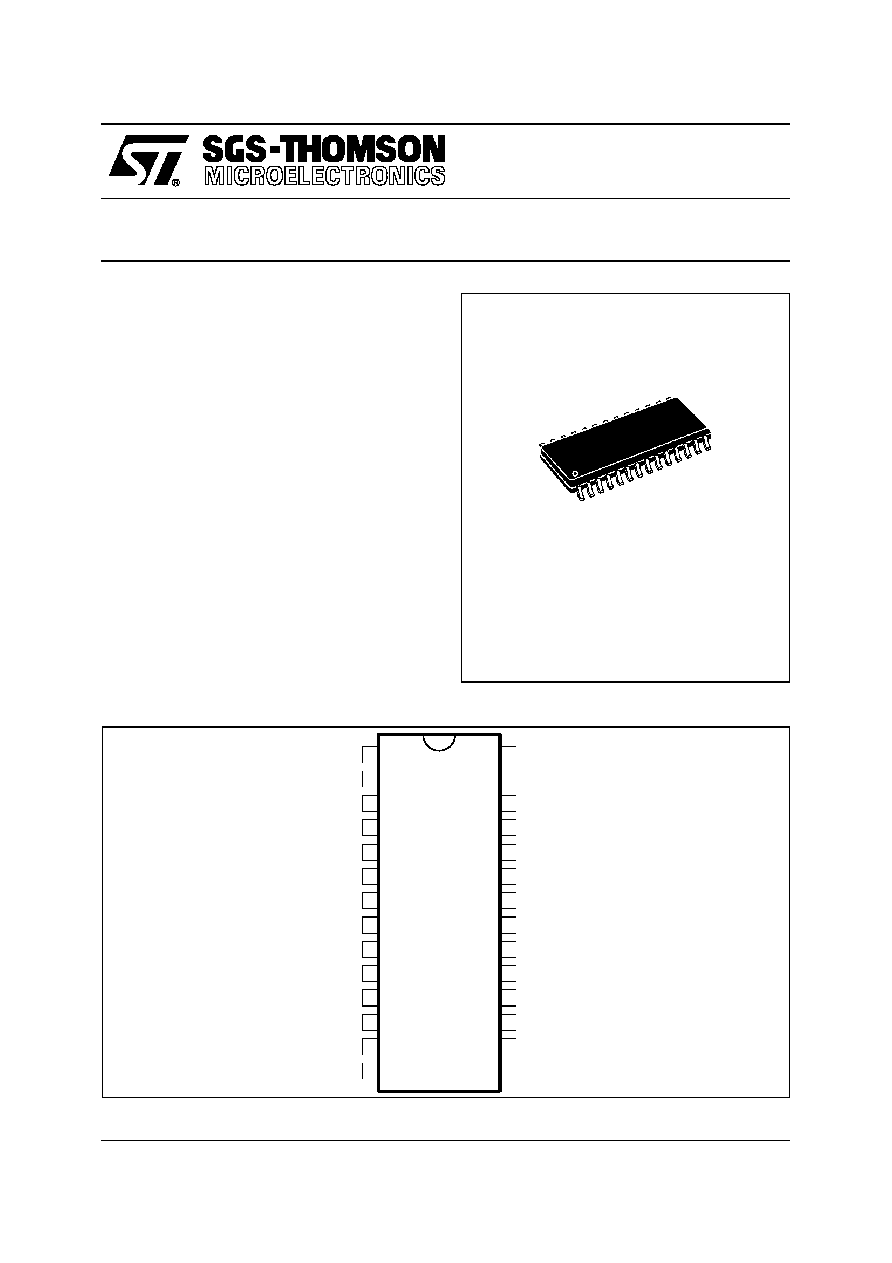
PIN CONNECTIONS
SO28
(Plastic Micropackage)
ORDER CODE : STV0190
.
RESOLUTION 6-BIT
.
MAX. SAMPLING FREQUENCY : 40 MSPS
.
TTL DATA OUTPUTS
.
BUILT-IN SAMPLING AND HOLD CIRCUIT
.
DUAL ADC ON CHIP TO IMPROVE CHAN-
NEL MATCHING
APPLICATIONS
.
QPSK DEMODULATION IN A SATELLITE
DECODER
This is advance information on a new product no w in development or undergoing evaluation. Deta ils are subject to change without notice.
DESCRIPTION
The STV0190 is a dual 40 MSPS 6-bit Analog to
Digital converter.
It is dedicated to QPSK demodulation in Satellite
receiver.
The Flash architecture combined with interpolation
technic gives the best trade off between power
consumption and maximum conversion speed.
1/7
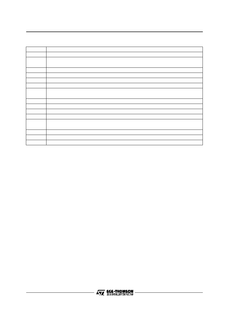
PIN CONFIGURATION
Pin N
�
Symbol
Function
1
V
CCO
Output Buffer Supply Voltage Channel A + B
2
OGND
Output Buffer Ground Channel A + B
3
AGND
Analog Ground
4
V
TOP
Top Reference Voltage
5
V
INA
Analog Input Channel A
6
V
MIDA
Reference Voltage DC Coupling Channel A
7
V
MIDB
Reference Voltage DC Coupling Channel B
8
V
INB
Analog Input Channel B
9
V
BOT
Bottom Reference Voltage
10
V
CCA
Analog Supply Voltage
11
DGND
Digital Ground
12
V
CCD
Digital Supply Voltage
13
CLKIN
Clock Input
14
OGND
Output Buffer Ground Channel A + B
15
V
CCO
Output Buffer Supply Voltage Channel A + B
16
CLKOUT
Clock Output
17 to 22
D0A to D5A
D0 (LSB) to D5 (MSB) Outputs Channel A
23 to 28
D0B to D5B
D0 (LSB) to D5 (MSB) Outputs Channel B
0190-01.TBL
STV0190
2/7

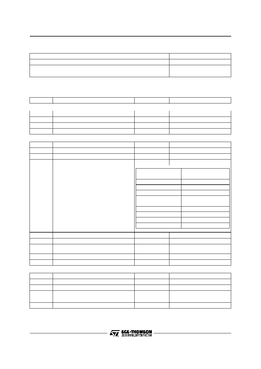
1
2
3
5
10
16
17
18
19
20
26
27
28
11
12
13
14
15
21
22
23
24
25
ADC A
6
ADC B
8
7
9
TTL
OUTP UT
LATCHES
TTL
OUTP UT
LATCHES
CLOCK
DRIVER
D5A
D4A
D3A
D2A
D1A
D0A
D5B
D4B
D3B
D2B
D1B
D0B
CLKOUT
CLKIN
AGND
DGND
OGND
V
CC O
V
CC D
V
CCA
V
INA
V
MIDA
V
INB
V
MIDB
V
BOT
4
V
TOP
S TV0190
0190-02.EPS
BLOCK DIAGRAM
STV0190
3/7
ABSOLUTE MAXIMUM RATINGS
Symbol
Parameter
Value
Unit
Analog Supply Voltage
3.1, 3.45
V
Digital Supply Voltage
3.1, 3.45
V
T
oper
Operating Temperature
0, +70
o
C
0190-02.TBL
ELECTRICAL CHARACTERISTICS (V
CC
= 3.3V, T
amb
= 0 to 70
o
C, Full scale 10MHz, 1.5V
PP
input,
40MSPS, C
L
= 20pF, unless otherwise specified)
Symbol
Parameter
Test Conditions
Min.
Typ.
Max.
Unit
ANALOG INPUT
Differential Reference Voltage
V
TOP
- V
BOT
1
1.5
V
PP
Variation of Channel A to Channel B (FS)
0.5 LSB
8
mV
R
IN
Input Resistance
20
k
Input Bandwidth 3dB
20
MHz
DIGITA L OUTPUTS
High Logic Voltage
2.4
V
CC
V
Low Logic Voltage
0
0.4
V
High Logic Current
-4
mA
Low Logic Current
4
mA
Logic Format
t
PD
Output Timing
See Figure 1
9
ns
t
V
Output Timing
See Figure 1
5
ns
t
SKEW
Data Output Skew TSK
(all outputs, settled within 20%)
See Figure 1
1
ns
t
APER
Aperture Delay relative to Data Clock
See Figure 1
1
ns
t
R
, t
F
Data Output Rise and Fall Time
4
ns
CLOCK INPUT
V
IH
High Input Voltage
2.0
V
CC
V
V
IL
Low Input Voltage
0
0.8
V
I
IH
High Input Current
TBD
�
A
I
IL
Low Input Current
TBD
�
A
Clock Duty Cycle
40
60
%
t
CL
Clock Period
See Figure 1
24
ns
0190-03.TBL
Analog Input
Digital Output
most positive input
63
111111
62
111110
....
............
33
100001
32
100000
31
011111
30
011110
....
............
1
000001
least positive input
0
000000
STV0190
4/7
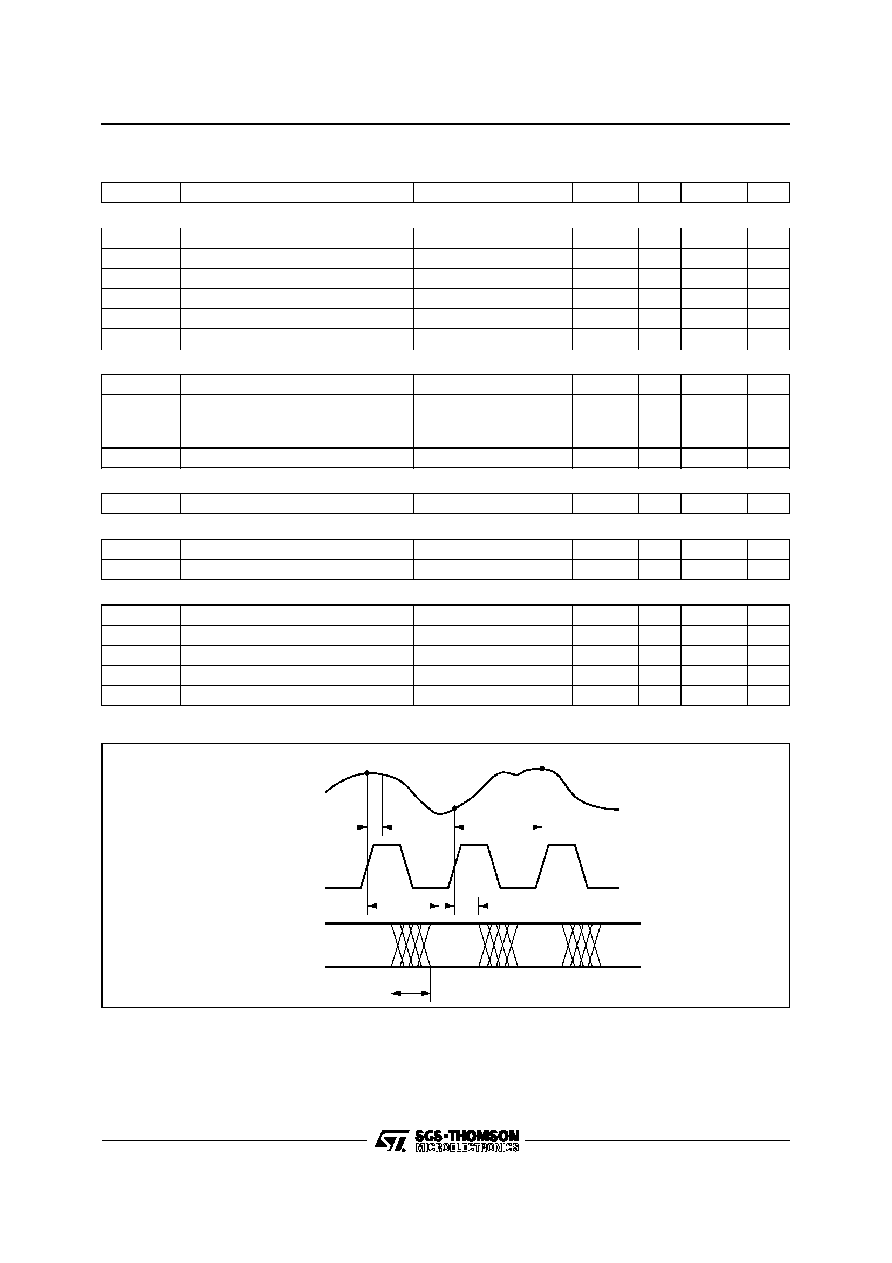
CLOCK OUT
S IGNAL
DIGITAL
S IGNAL
ANALO G
S IGNAL
t
APER
t
P D
t
V
t
CL
N
N+1
N+2
Da ta
for N
Da ta
for N+1
Da ta
for N+2
t
S KEW
0190-03.EPS
Note : This diagram shows a delay of one clock cycle. Additionnal integer multiple delay periods are acceptable. Output data must be valid on
the rising edge of the clock out signal.
Figure 1 : Timing Diagram
ELECTRICAL CHARACTERISTICS (continued)
Symbol
Parameter
Test Conditions
Min.
Typ.
Max.
Unit
CLOCK OUTPUT
V
OH
High Ouput Voltage
2.4
V
CC
V
V
OL
Low Output Voltage
0
0.4
V
I
OH
High Output Current
-4
mA
I
OL
Low Output Current
4
mA
Clock Duty Cycle
40
60
%
t
CL
Clock Period
24
ns
REFERENCE LADDER
Top Voltage
V
CC
- 0.5
V
Bottom Voltage
V
CC
+ 0.5
V
DC Bias Restoration Error
Open input digital output
should be
32/64
011111
33/64
100000
ZV
TOP
/V
BOT
Input Impedance
90
CROSSTALK
Isolation A/B
37
dB
DC ACCURACY
Integral non Lin.
-0.5
+0.5
LSB
Diff. Non Lin.
-0.5
+0.5
LSB
AC ACCURACY (f
IN
= 10MHz, FS = 40 MSPS, V
IN
= 95% FSCALE)
Effective Number of Bit
5
bits
SNR
33
dB
THD
THD First 5 Harmony
33
dB
Integral non Lin.
-1
+1
LSB
A/D Amplifier Response Mismatching
0.2
dB
0190-04.TBL
STV0190
5/7