STV0196B
QPSK/BPSK DEMODULATOR AND FEC IC
September 1996
PQFP64
(Plastic Package)
ORDER CODE : STV0196B
FRONT-END INTERFACE
.
I AND Q 6 BITS DIGITAL INPUTS AT 2Fs
.
QPSK DEMODULATION (Two Modes : A and B)
.
INPUT SYMBOL FREQUENCY (Fs)
UP TO
30MSYMBOLS/S
.
DIGITAL NYQUIST ROOT FILTER :
ROLL-OFF VALUE OF 0.35 IN MODE A
.
DIGITAL CARRIER LOOP :
- ON-CHIP DEROTATOR AND TRACKING
LOOP
- CARRIER OFFSET INDICATOR
- LOCK DETECTOR
- C/N INDICATOR FOR DISH POSITIONING
.
DIGITAL TIMING RECOVERY :
- INTERNAL TIMING ERROR EVALUATION
AND FILTER
- OUTPUT CONTROL SIGNAL FOR A 2Fs
EXTERNAL VCO OR VCXO
.
DIGITAL AGC :
- INTERNAL SIGNAL POWER ESTIMATION
AND FILTER
- OUTPUT CONTROL SIGNAL FOR AGC
(1 BIT PULSE DENSITY MODULATION)
FORWARD ERROR CORRECTION
.
INNER DECODER :
- VITERBI SOFT DECODER FOR CONVOLU-
TIONAL CODES, CONSTRAINT LENGTH
M = 7, RATE 1/2
- PUNCTURED CODES 1/2, 2/3, 3/4, 5/6 AND
7/8 IN MODE A
- AUTOMATIC OR MANUAL RATE AND
PHASE RECOGNITION
.
DEINTERLEAVER :
- WORD SYNCHRO EXTRACTION
- CONVOLUTIVE DEINTERLEAVER
.
OUTER DECODER :
- IN MODE A : REED-SOLOMON DECODER
FOR 16 PARITY BYTES ; CORRECTION OF
UP TO 8 BYTE ERRORS
- BLOCK LENGTHS : 204 IN MODE A
- ENERGY DISPERSAL DESCRAMBLER
CONTROL
.
I
2
C SERIAL BUS
DESCRIPTION
Designed for the fast growing direct broadcast
satellite
(DBS) digital TV receiver market,
the SGS-THOMSON STV0196B Digital Satellite
Receiver Front-end integrates all the functions
needed to demodulate incoming digital satellite TV
signals from the tuner : Nyquist filters, QPSK/BPSK
demodulator, signal power estimator, automatic
gain control, Viterbi decoder, deinterleaver, Reed-
Solomon decoder and energy dispersal descram-
bler. This high level of integration greatly reduces
the package count and cost of a set top box. The
demodulator blocks are suitable for a wide range
of symbol rates while the advanced error correction
functions guarantee a low error rate even with small
receiver antennas or low power transmitters.
The STV0196B has multistandard capability.
It is fully compliant with the recently defined Digital
Video Broadcasting (DVB) standard (already
adopted by satellite TV operators in the USA,
Europe and Asia) and also compatible with the
main consumer digital satellite TV standards in use.
1/23
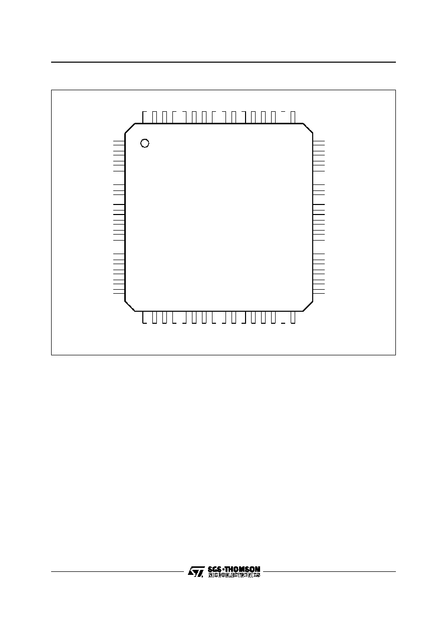
17 18 19 20 21 22 23 24 25 26 27 28 29 30 31 32
64 63 62 61 60 59 58 57 56 55 54 53 52 51 50 49
48
47
46
45
44
43
42
41
40
39
38
37
36
35
34
33
16
15
14
13
12
11
10
9
8
7
6
5
4
3
2
1
TE ST
V
S S
V
DD
TE ST
TE ST
TE ST
TE ST
TE ST
TE ST
TE ST
V
S S
V
S S
V
S S
V
DD
V
DD
V
DD
V
DD
V
S S
V
S S
V
S S
V
DD
V
DD
M_C LK
MODE
CLKREC
AGC
SDA
SCL
NRES
D60
ERROR
D/P
TEST
TEST
V
SS
V
DD
Q0
Q1
Q2
Q3
Q4
Q5
I0
I1
I2
I3
I4
I5
V
SS
V
DD
TEST
TEST
D0
D1
D2
D3
D4
D5
D6
D7
V
SS
V
DD
CK_OUT
STR_OUT
0196B-01.EPS
PIN CONNECTIONS
STV0196B
2/23

PIN LIST
Pin Number
Pin Name
Type
Pin Description
SIGNAL INPUTS
51, 52, 53, 54, 55, 56
I [5..0]
I
In Phase Component, at twice the symbol frequency (2Fs).
57, 58, 59, 60, 61, 62
Q [5..0]
I
In Quadrature Component, at twice the symbol frequency (2Fs).
48
M_CLK
I
Master Clock Input, 2Fs. Sampling Clock of the External A to D Converters.
FRONT END CONTROLS
46
CLKREC
O
1 Bit Control Signal for the External CLK VCO. It must be Low-pass Filtered.
44
AGC
O
1 Bit Control Signal for the External AGC. It must be Low-pass Filtered.
35
D60
O
M_CLK Divided by 60
SIGNAL OUTPUTS
26, 25, 24, 23,
22, 21, 20, 19
D [7..0]
O
Output Data
29
CK_OUT
O
Output Byte Clock
30
STR_OUT
O
Output Synchronization Byte Signal
33
D/P
O
Data/Parity Signal
34
ERROR
O
Output Error Signal. Set in Case of uncorrected Block.
I
2
C MICRO INTERFACE
39
SCL
I
Serial Clock
40
SDA
I/O
Serial Data Bus
OTHER
47
MODE
I
0 = Mode A, 1 = Mode B
1, 2, 5, 6, 13, 14, 15,
16, 17, 18, 63, 64
TEST
O
Reserved for Manufacturing Test. It must remain unconnected
3, 7, 9, 11, 28, 32,
37, 41, 42, 49
V
SS
I
Ground References
4, 8, 10, 12, 27,
31, 38, 43, 45, 50
V
DD
I
3.3V Supply
36
NRES
I
Negative Reset
0196B-01.TBL
VITERBI DECODER
DEINTERLEAVER
REED SOLOMON DECODER
ENERGY DESCRAMBLER
NYQUIST
FILTER
DEROTATOR
AGC
LOCK
INDICATOR
DCO
TIMING
RECOVERY
CARRIER
OFFSET
MEASURE
CARRIER PHASE
TRACKING LOOP
DIVIDE BY 60
I
2
C BUS
INTERFACE
AGC
D/P
ERROR
STR_OUT
CK_OUT
I[5...0]
Q[5...0]
CLKREC
D60
M_CLK
SCL
SDA
MODE
V
DD
V
SS
D[7..0]
STV0196B
C/N
INDICATOR
0196B-02.EPS
BLOCK DIAGRAM
STV0196B
3/23
FUNCTIONAL DESCRIPTION
I - I
2
C BUS SPECIFICATION
This is the standard I
2
C protocol.
The device address is "1101000" ; the first byte is therefore Hex D0 for a write operation and Hex D1 for a
read operation.
I.1 - Write Operation
The first byte is the device address plus the direction bit (R/W = 0).
The second byte contains the internal address of the first register to be accessed.
The next byte is written in the internal register.
The following (if any) bytes are written in successive internal registers.
The transfer lasts until stop conditions are encountered.
The STV0196B acknowledges every byte transfer.
I.2 - Read Operation
The address of the first register to read is programmed in a write operation without data, and terminated
by stop condition.
Then another start is followed by the device address and R/W = 1 ; all successive bytes are now data read
at successive positions starting from the initial address.
The STV0196B acknowledges every byte transfer.
Example :
Write registers 0 to 3 with AA,BB,CC,DD
Start
Device Address,
Write D0
ACK
Internal
Address
ACK
Data
AA
ACK
Data
BB
ACK
Data
CC
ACK
Stop
Read registers 2 and 3
Start
Device Address,
Write D0
ACK
Register Address 01
ACK
Stop
Start
Device Address,
Read D1
ACK
Data Read
BB
ACK
Data Read
CC
ACK
Stop
I.3 - Identification Register
This read only register gives the release number of the circuit in order to ensure software compatibility.
The read value is Hex 83 for STV0196B and Hex 81 for STV0196.
Internal Address : Hex 0B
1
0
0
0
0
0
1
1
Notes : - Unspecified register addresses must not be used.
- All the unused bits in the registers must be programmed to 0.
STV0196B
4/23

I.4 - Register Map
FUNCTIONAL DESCRIPTION (continued)
REGISTER HEX 00
INPUT CONFIGURATION REGISTER (R/W)
Reset Value : Hex 04
0
-Q(1) or Q(0) input
1
Signed (1) or positive (0) I & Q inputs
2
Nyquist filtering on (1) / off (0)
3
BPSK (1), QPSK(0)
4
To be set to 0.
5
To be set to 0.
6
To be set to 0.
7
To be set to 0.
REGISTERS HEX 01 TO HEX 05
VITERBI, PUNCTURE RATE THRESHOLDS (R/W)
Reset Value : Hex 20
rate
Hex01 VTH0 0 Th6 Th5 Th4 Th3 Th2 Th1 Th0 1/2
Hex02 VTH1 0 Th6 Th5 Th4 Th3 Th2 Th1 Th0 2/3
Hex03 VTH2 0 Th6 Th5 Th4 Th3 Th2 Th1 Th0 3/4
Hex04 VTH3 0 Th6 Th5 Th4 Th3 Th2 Th1 Th0 5/6
Hex05 VTH4 0 Th6 Th5 Th4 Th3 Th2 Th1 Th0
7/8
or
6/7
REGISTER HEX 06
VSEARCH (VITERBI) (R/W)
Reset Value : Hex 19
0
H[1..0]
Sync counter hysteresis value
1
2
T[1..0]
Sync search time out
3
4
SN[1..0]
VITERBI error rate averaging period.
C/N indicator averaging period.
5
6
F
VITERBI operating status freeze (1)
7
A/M
(0) automatic, (1) manual
REGISTER HEX 07
VERROR REGISTER (Read only)
REGISTER HEX 08
VSTATUS REGISTER (Read only)
0
PR[2..0] Current puncture rate identification
1
2
3
LK
(1) synchro found,
(0) searching puncture rate
4
PRF
(1) puncture rate found,
(0) searching puncture rate
5
unused set to (0)
6
unused set to (0)
7
CF
(1) carrier found, (0) searching carrier
REGISTER HEX 09
PUNCTURE RATE ENABLE (R/W)
Reset Value : Hex 10 (mode A)
0
E0
(1) Puncture 1/2 enabled, (0) disabled
1
E1
(1) Puncture 2/3 enabled, (0) disabled
2
E2
(1) Puncture 3/4 enabled, (0) disabled
3
E3
(1) Puncture 5/6 enabled, (0) disabled
4
E4
(1) Puncture7/8 (mode A), 6/7 (mode B)
(0) disabled
5
unused
6
7
REGISTER HEX 0A
RS REGISTER (R/W)
Reset Value : Hex B8
0 RS0 (1) output clock stopped during parity,
(0) continuous
1 RS1 Output clock polarity
2 RS2 (1) all synchro words are Hex47,
(0) synchro inversion disabled
3 RS3 Write error bit
4 RS4 Descrambler on (1), off (0)
5 RS5 Reed-Solomon on (1), off (0)
6 RS6 Normal operation (0), Reed-Solomon
correction bytes to output (1)
7 RS7 De-interleaver on (1), off (0)
STV0196B
5/23