May 2000
1/36
This is preliminary information on a new product now in development or undergoing evaluation. Details are subject to change without notice.
STV0299B
QPSK/BPSK LINK IC
s
MULTISTANDARD
QPSK
AND BPSK
DEMODULATION
s
EASY IMPLEMENTATION WITH LOW COST
DIRECT CONVERSION TUNERS
s
EXTREMELY LOW BER WHEN
CO-CHANNEL INTERFERENCE
s
WIDE CARRIER LOOP TRACKING RANGE TO
COMPENSATE FOR DISH FREQUENCY DRIFT
s
COMMON INTERFACE COMPLIANT
s
VERY LOW POWER CONSUMPTION
s
INTEGRATED DUAL 6-BIT ANALOG TO
DIGITAL CONVERTERS
s
DUAL DIGITAL AGC
s
DIGITAL NYQUIST ROOT FILTER WITH
ROLL-OFF OF 0.35 OR 0.20
s
DIGITAL CARRIER LOOP WITH LOCK
DETECTOR, ON-CHIP WIDE RANGE
DEROTATOR AND TRACKING LOOP
(TYP � 45 MHz)
s
DIGITAL TIMING RECOVERY WITH LOCK
DETECTOR
s
CHANNEL BIT RATE UP TO 90 Mbps AND
SYMBOL FREQUENCY RATE FROM
1 TO 50 MSYMBOLS
s
INNER DECODER:
- VITERBI SOFT DECODER FOR
CONVOLUTIONAL CODES, M=7, RATE 1/2
- PUNCTURED CODES 1/2, 2/3, 3/4, 5/6, 6/7 AND 7/8
s
SYNCHROWORD EXTRACTION
s
CONVOLUTIVE DEINTERLEAVER
s
OUTER DECODER:
- REED-SOLOMON DECODER FOR
16 PARITY BYTES; CORRECTION OF UP
TO 8 BYTE ERRORS
- ENERGY DISPERSAL DESCRAMBLER
s
ON-CHIP FLEXIBLE CLOCK SYSTEMS TO
ALLOW USE OF EXTERNAL CLOCK
SIGNALS IN 4 MHz TO 30 MHz RANGE
s
EASY-TO-USE C/N ESTIMATOR WITH 2 TO
18 dB RANGE
s
I
2
C SERIAL BUS AND REPEATER
s
DVB COMMON INTERFACE COMPLIANT
PARALLEL OUTPUT FORMAT
s
PARALLEL AND SERIAL DATA OUTPUT
s
LNB SUPPLY CONTROL WITH STANDARD I/O,
22 KHz TONE AND DISEQC
TM
MODULATOR
WITH TTL OUTPUT
s
CMOS TECHNOLOGY: 2.5 V OPERATION;
JEDEC (EIA/JESD8-5)
APPLICATIONS
s
DIGITAL SATELLITE RECEIVER AND
SET-TOP BOXES
DESCRIPTION
The STV0299 Satellite Receiver with FEC is a
CMOS single-chip multistandard demodulator for
digital satellite broadcasting. It consists of two A/D
converters for I-input and Q-input, a multistandard
QPSK and BPSK demodulator, and a forward
error correction (FEC) unit having both an inner
(Viterbi) and outer (Reed-Solomon) decoder.
The FEC unit is compliant with the DVB-S and
DSS
TM
specifications. Processing is fully digital.
It integrates a derotator before the Nyquist root
filter, allowing a wide range of offset tracking.
The high sampling rate facilitates the
implementation of low-cost, direct conversion
tuners.
A variety of configurations and behaviours can be
selected through a bank of control/configuration
registers via an I
2
C. The chip outputs MPEG
Transport Streams and interfaces seamlessly to
the Packet Demultiplexers embedded in ST's
ST20-TPx or STi55xx. High sampling frequency
(up to 90MHz) considerably reduces the cost of
LPF of direct conversion tuners.
The multistandard capability associated with a
broad range of input frequency operations makes
it easy-to-use. Its low power consumption, small
package and optional serial output interface
makes it perfect for embedding into a tuner.
TQFP64 (10 x 10 x 1.4 mm)
(Thin Plastic Quad Flat Pack)
ORDER CODE: STV0299B (No Slug)

STV0299B
2/36
Page
TABLE OF CONTENTS
1 PIN INFORMATION . . . . . . . . . . . . . . . . . . . . . . . . . . . . . . . . . . . . . . . . . . . . . . . . . . . . . . . . . . . . . . 4
1.1 Pin Connections . . . . . . . . . . . . . . . . . . . . . . . . . . . . . . . . . . . . . . . . . . . . . . . . . . . . . . . . . . . 4
1.2 Pinout Description. . . . . . . . . . . . . . . . . . . . . . . . . . . . . . . . . . . . . . . . . . . . . . . . . . . . . . . . . . 5
2 BLOCK DIAGRAM . . . . . . . . . . . . . . . . . . . . . . . . . . . . . . . . . . . . . . . . . . . . . . . . . . . . . . . . . . . . . . . 6
3 SYSTEM CHARACTERISTICS . . . . . . . . . . . . . . . . . . . . . . . . . . . . . . . . . . . . . . . . . . . . . . . . . . . . . 6
4 FUNCTIONAL DESCRIPTION . . . . . . . . . . . . . . . . . . . . . . . . . . . . . . . . . . . . . . . . . . . . . . . . . . . . . . 7
4.1 Front End Interfaces . . . . . . . . . . . . . . . . . . . . . . . . . . . . . . . . . . . . . . . . . . . . . . . . . . . . . . . . 7
4.1.1 I
2
C Interface . . . . . . . . . . . . . . . . . . . . . . . . . . . . . . . . . . . . . . . . . . . . . . . . . . . . . . . . . . . 7
4.1.2 Write Operation (Normal Mode) . . . . . . . . . . . . . . . . . . . . . . . . . . . . . . . . . . . . . . . . . . . . 7
4.1.3 Read Operation (Normal Mode). . . . . . . . . . . . . . . . . . . . . . . . . . . . . . . . . . . . . . . . . . . . 7
4.1.4 I
2
C Interface in Standby Mode . . . . . . . . . . . . . . . . . . . . . . . . . . . . . . . . . . . . . . . . . . . . . 7
4.1.5 Specific Concerns about SCL Frequency . . . . . . . . . . . . . . . . . . . . . . . . . . . . . . . . . . . . 8
4.1.6 Identification Register. . . . . . . . . . . . . . . . . . . . . . . . . . . . . . . . . . . . . . . . . . . . . . . . . . . . 8
4.1.7 Sampling Frequency . . . . . . . . . . . . . . . . . . . . . . . . . . . . . . . . . . . . . . . . . . . . . . . . . . . . 8
4.1.8 Clock Generation . . . . . . . . . . . . . . . . . . . . . . . . . . . . . . . . . . . . . . . . . . . . . . . . . . . . . . . 8
4.1.9 Clock Registers . . . . . . . . . . . . . . . . . . . . . . . . . . . . . . . . . . . . . . . . . . . . . . . . . . . . . . . 10
4.1.10 I2C Bus Repeater. . . . . . . . . . . . . . . . . . . . . . . . . . . . . . . . . . . . . . . . . . . . . . . . . . . . . 10
4.1.11 General Purpose
DAC . . . . . . . . . . . . . . . . . . . . . . . . . . . . . . . . . . . . . . . . . . . . . . 10
4.1.12 DiSEqC Interface . . . . . . . . . . . . . . . . . . . . . . . . . . . . . . . . . . . . . . . . . . . . . . . . . . . . . 10
4.1.13 Standby Mode . . . . . . . . . . . . . . . . . . . . . . . . . . . . . . . . . . . . . . . . . . . . . . . . . . . . . . . 11
4.2 Signal Processing . . . . . . . . . . . . . . . . . . . . . . . . . . . . . . . . . . . . . . . . . . . . . . . . . . . . . . . . . 12
4.2.1 I and Q Inputs. . . . . . . . . . . . . . . . . . . . . . . . . . . . . . . . . . . . . . . . . . . . . . . . . . . . . . . . . 12
4.2.2 Main AGC (or AGC1) . . . . . . . . . . . . . . . . . . . . . . . . . . . . . . . . . . . . . . . . . . . . . . . . . . . 12
4.2.3 Nyquist Root and Interpolation Filters . . . . . . . . . . . . . . . . . . . . . . . . . . . . . . . . . . . . . . 12
4.2.4 Offset Cancellation . . . . . . . . . . . . . . . . . . . . . . . . . . . . . . . . . . . . . . . . . . . . . . . . . . . . . 12
4.2.5 Signal AGC (or AGC2) . . . . . . . . . . . . . . . . . . . . . . . . . . . . . . . . . . . . . . . . . . . . . . . . . . 12
4.3 Timing Recovery . . . . . . . . . . . . . . . . . . . . . . . . . . . . . . . . . . . . . . . . . . . . . . . . . . . . . . . . . . 13
4.3.1 Timing Control . . . . . . . . . . . . . . . . . . . . . . . . . . . . . . . . . . . . . . . . . . . . . . . . . . . . . . . . 13
4.3.2 Loop Equation . . . . . . . . . . . . . . . . . . . . . . . . . . . . . . . . . . . . . . . . . . . . . . . . . . . . . . . . 13
4.3.3 Timing Lock Indicator . . . . . . . . . . . . . . . . . . . . . . . . . . . . . . . . . . . . . . . . . . . . . . . . . . . 13
4.4 Carrier Recovery and Derotator Loop . . . . . . . . . . . . . . . . . . . . . . . . . . . . . . . . . . . . . . . . . 14
4.4.1 Loop Parameters . . . . . . . . . . . . . . . . . . . . . . . . . . . . . . . . . . . . . . . . . . . . . . . . . . . . . . 14
4.4.2 Carrier Lock Detector . . . . . . . . . . . . . . . . . . . . . . . . . . . . . . . . . . . . . . . . . . . . . . . . . . . 14
4.4.3 Derotator Frequency . . . . . . . . . . . . . . . . . . . . . . . . . . . . . . . . . . . . . . . . . . . . . . . . . . . 14
4.4.4 Carrier Frequency Offset Detector . . . . . . . . . . . . . . . . . . . . . . . . . . . . . . . . . . . . . . . . . 14
4.5 Noise Indicator. . . . . . . . . . . . . . . . . . . . . . . . . . . . . . . . . . . . . . . . . . . . . . . . . . . . . . . . . . . . 14
4.6 Forward Error Correction . . . . . . . . . . . . . . . . . . . . . . . . . . . . . . . . . . . . . . . . . . . . . . . . . . . 15
4.6.1 FEC Modes . . . . . . . . . . . . . . . . . . . . . . . . . . . . . . . . . . . . . . . . . . . . . . . . . . . . . . . . . . 15
4.6.2 Viterbi Decoder and Synchronization . . . . . . . . . . . . . . . . . . . . . . . . . . . . . . . . . . . . . . . 15
4.6.3 Synchronization . . . . . . . . . . . . . . . . . . . . . . . . . . . . . . . . . . . . . . . . . . . . . . . . . . . . . . . 16
4.6.4 Error Monitoring . . . . . . . . . . . . . . . . . . . . . . . . . . . . . . . . . . . . . . . . . . . . . . . . . . . . . . . 16
4.6.5 Convolutional Deinterleaver . . . . . . . . . . . . . . . . . . . . . . . . . . . . . . . . . . . . . . . . . . . . . . 16
4.6.6 Reed-Solomon Decoder and Descrambler . . . . . . . . . . . . . . . . . . . . . . . . . . . . . . . . . . 16
4.6.7 Parallel Output Interface . . . . . . . . . . . . . . . . . . . . . . . . . . . . . . . . . . . . . . . . . . . . . . . . 16
4.6.8 Serial Output Interface . . . . . . . . . . . . . . . . . . . . . . . . . . . . . . . . . . . . . . . . . . . . . . . . . . 17
5 REGISTER LIST. . . . . . . . . . . . . . . . . . . . . . . . . . . . . . . . . . . . . . . . . . . . . . . . . . . . . . . . . . . . . . . . 19
6 ELECTRICAL CHARACTERISTICS . . . . . . . . . . . . . . . . . . . . . . . . . . . . . . . . . . . . . . . . . . . . . . . . 29
6.1 Absolute Maximum Ratings . . . . . . . . . . . . . . . . . . . . . . . . . . . . . . . . . . . . . . . . . . . . . . . . . 29

STV0299B
3/36
Page
TABLE OF CONTENTS (continued)
6.2 Thermal Data . . . . . . . . . . . . . . . . . . . . . . . . . . . . . . . . . . . . . . . . . . . . . . . . . . . . . . . . . . . . . 29
6.3 DC Electrical Characteristics . . . . . . . . . . . . . . . . . . . . . . . . . . . . . . . . . . . . . . . . . . . . . . . . 29
6.4 Timing Characteristics . . . . . . . . . . . . . . . . . . . . . . . . . . . . . . . . . . . . . . . . . . . . . . . . . . . . . 31
6.5 I
2
C Bus Characteristics. . . . . . . . . . . . . . . . . . . . . . . . . . . . . . . . . . . . . . . . . . . . . . . . . . . . . 32
7 APPLICATION BLOCK DIAGRAMS . . . . . . . . . . . . . . . . . . . . . . . . . . . . . . . . . . . . . . . . . . . . . . . . 33
8 PACKAGE MECHANICAL DATA . . . . . . . . . . . . . . . . . . . . . . . . . . . . . . . . . . . . . . . . . . . . . . . . . . 35
STV0299B
4/36
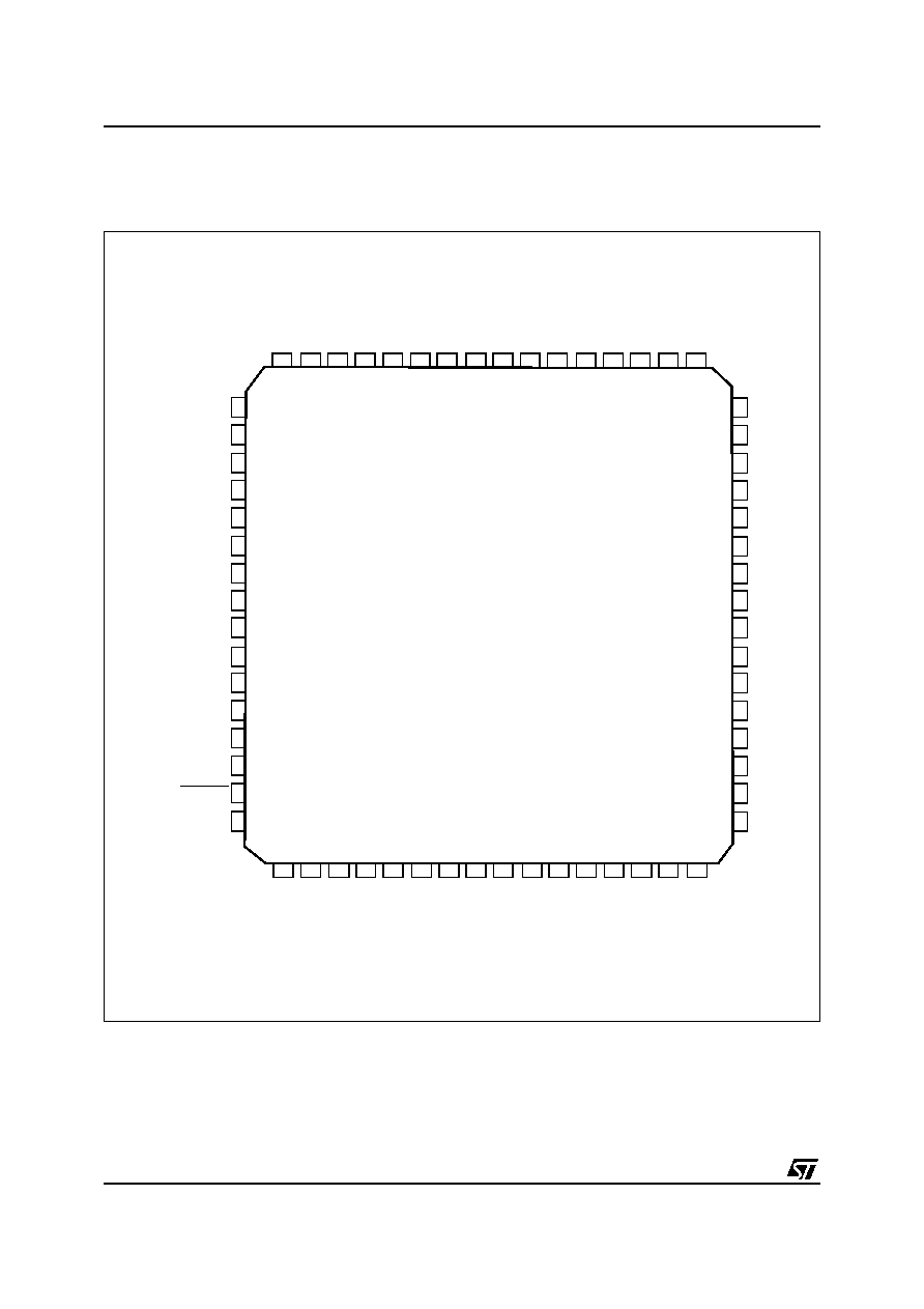
1
PIN INFORMATION
1.1 Pin Connections
Figure 1:
Pinout for 64-pin TQFP (10x10 mm)
V
DD
QN
QP
V
DD
A
V
TO
P
V
SS
A
DI
RCL
K-DI
S
SCL
T
V
SS
SDAT
IP
IN
V
SS
A
V
SS
A
TEST
V
SS
V
DD
D/
P
V
SS
CL
K_
OUT
V
DD
_3
.
3
V
SER
IAL D
A
TA
/D7
D6
D5
OP
1
LO
C
K
/O
P
2
ERR
O
R
OP
0
F22/DiSEqC
SCL
V
DD
CLK_IN/XTAL_IN
XTAL_OUT
V
DDA
RESET
D3
STDBY
TEST
V
DDA
TEST
TEST
V
BOT
1
2
3
4
5
6
7
8
9
10
11
12
13
14
15
16
48
47
46
45
44
43
42
41
40
39
38
37
36
35
34
33
64
62
61
60
59
58
57
56
55
63
54
53
52
51
50
49
17
19
20
21
22
23
24
25
26
18
27
28
29
30
31
32
V
SS
V
SSA
V
SS
V
SS
SDA
V
DD_3.3 V
TEST
TEST
V
DD
DAC
V
SS
IP0
D0
D1
D2
D4
STR
_
OUT
TEST
V
DD
V
SS
AUX_CLK
AGC
STV0299B
5/36
1
PIN INFORMATION (continued)
1.2 Pinout Description
Note:
1
The following abbreviations are used: I - Input; O - Output; OD - Open drain output.
2
3.3 V output levels.
3
5 V tolerant
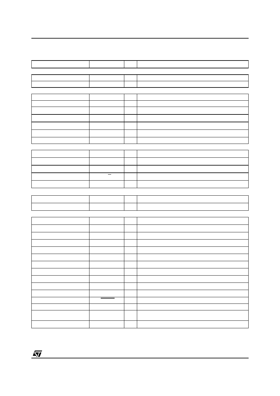
Pin Number
Name
I/O
1
Description
SIGNAL INPUTS
50, 51
IP, IN
I
Analog in Phase Component
53, 54
QN, QP
I
Analog in Quadrature Component
FRONT END CONTROLS
1
CLK_IN/XTAL IN
I
Crystal Input or CLK_IN
2
XTAL OUT
O
Crystal Output
9
AGC
OD
3
Control Signal to the Tuner
5
AUX_CLK
O
2
Programmable Output Port or Programmable Output Clock
17-18
OP0, OP1
O
2
Programmable Output Ports
19
LOCK/OP2
O
2
Carrier Found or Data Found or Output Port
38
IP0
I
Input Port
SIGNAL OUPUTS
26-28-29-31, 33 to 36
D[7:0]
O
2
Output Data; D7 is DATA_OUT in Serial Mode
24
CLK_OUT
O
2
Output Byte Clock; or Bit Clock in Serial Mode
22
STR_OUT
O
2
Output 1st byte Signal (synchro byte clock)
21
D/P
O
2
Data/Parity Signal
20
ERROR
O
2
Output Error Signal. Set in case of uncorrectible packet.
I
2
C INTERFACE
14
SCL
I
3
Serial Clock (I
2
C bus)
12
SDA
I/OD
3
Serial Data (I
2
C bus)
OTHERS
59
SCLT
OD
3
Tuner Serial Clock (repeator) or Output Port
60
SDAT
I/OD
3
Tuner Serial Data (repeator) or Input/Output Port
37-43-44-45-46-61-62
TEST
I
Reserved for manufacturing tests; must be tied to V
SS
58
DIRCLK_DIS
I
Sets the DIRCLK function at power on
3, 49, 52, 57
V
SSA
S
Analog Ground
4, 47, 55
V
DDA
S
Analog 2.5 V Supply
56
V
TOP
S
ADC High Voltage Reference
48
V
BOT
S
ADC Low Voltage Reference
6-8-11-23-27-32-39-64
V
SS
S
Ground
13-25
V
DD_3.3 V
S
3.3 V Supply
7-10-30-41-63
V
DD
S
2.5 V Supply
15
RESET
I
Reset, active at low level
42
STDBY
I
Sets STDBY at power on
16
F22/DiSEqC
O
2
DiSEqC modulation, 22 kHz Tone, Programmable
Output Port
40
DAC
O
2
Programmable Digital to Analog Converter Output