STV0502
CCD SENSORS ANALOG PROCESSOR IC
October 1998
.
SERIAL BUS CONTROL
VIDEO
.
CORRELATED DOUBLE SAMPLING OF THE
CCD SIGNAL
.
DIGITALLY CONTROLLED VARIABLE AMPLI-
FIER AND BLACK CLAMP LEVEL
.
8 BITS PIXEL RATE ADC
AUDIO
.
MICROPHONE PREAMP WITH SWITCHABLE
AGC (RANGE 34dB - 60dB) OR FIXED GAIN
DESCRIPTION
The chip integrates the analog functions needed in
a CCD Video Camera, more particularly for video-
conferencing purpose.
The CCD signal is sampled, amplified to a useful
level and digitized by an 8 bits ADC. The gain of the
amplifier and the black level clamp can be adjusted
by a serial bus.
The audio microphone preamplifier allows a micro-
phone to be connected to the chip, which outputs
a differential audio line level signal ready for digital
conversion or straight amplification. The preampli-
fier incorporates an AGC to adapt to the income
signal level. The AGC is switchable ON/OFF by the
serial interface.
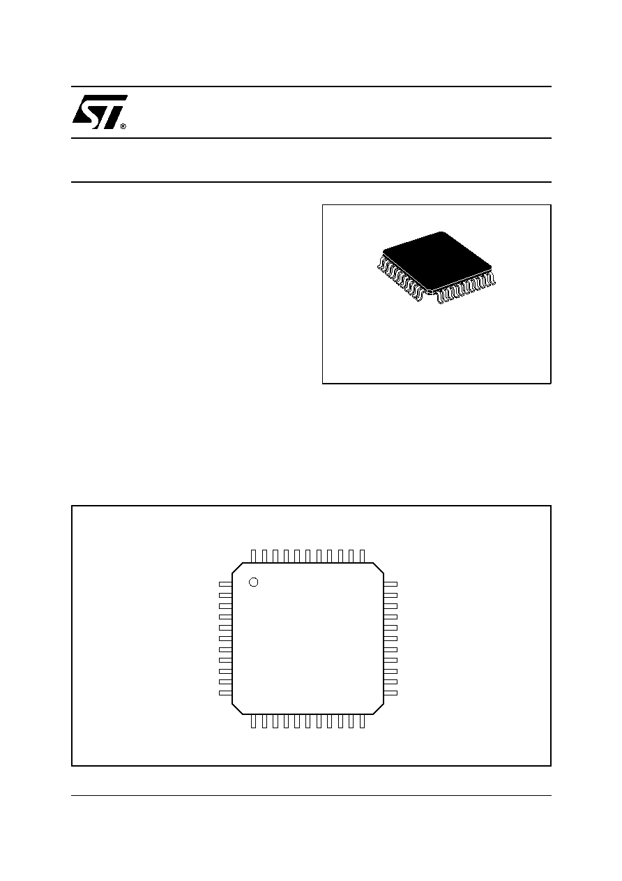
TQFP44 Full (10 x 10 x 1.40mm)
(Plastic Quad Flat Pack)
ORDER CODE : STV0502
33
32
31
30
29
1
2
3
4
5
40
41
42
43
44
18 19 20 21 22
DATA6
DATA5
DATA4
AF_OUT-
AF_OUT+
V
CC
CAGC
V
CC
GN
D
SDATA_IO
V
SS
OB
FCDS
FS
8
9
10
11
7
6
16 17
14 15
12 13
28
27
26
25
24
23
39 38 37 36 35 34
SCLK
ADC_CLOCK
GND
MICRO_IN
MIC_REF
ACC
V
BIAS
V
DD
DATA0
DATA1
DATA2
DATA3
V
DD
DATA7
NOT USED
NOT USED
V
SS
VAGCIN
CDS_OUT
CDS_REF
CDS_IN
GN
D
V
CC
V
TO
P
V
BOT
BLACK_REF
NOT USED
OB_
C
AP
AGC LEVEL
TEST ONLY
05
02
-
0
1.
E
P
S
PIN CONNECTIONS
1/15

PINOUT DESCRIPTION
Pin
Signal
Ana./Dig.
Type
Description
1
VAGCIN
Analog
I
Video Variable Gain Input
2
CDS_OUT
Analog
O
CDS Output
3
CDS_REF
Analog
-
CDS Reference
4
CDS_IN
Analog
I
CDS Input
5
V
SS
Digital
-
ADC Data Ground
8
DATA[7]
Digital
O
ADC Output - MSB
9
DATA[6]
Digital
O
ADC Output
10
DATA[5]
Digital
O
ADC Output
11
DATA[4]
Digital
O
ADC Output
12
DATA[3]
Digital
O
ADC Output
13
DATA[2]
Digital
O
ADC Output
14
DATA[1]
Digital
O
ADC Output
15
DATA[0]
Digital
O
ADC Output - LSB
16
V
DD
Digital
-
ADC Data Supply
17
V
DD
Digital
-
Digital Supply
18
SDATA_IO
Digital
I/O
Serial Interface Data Wire
19
V
SS
Digital
-
Digital Ground
20
OB
Digital
I
OB Pulse
21
FCDS
Digital
I
FCDS Pulse
22
FS
Digital
I
FS Pulse
23
SCLK
Digital
I
Serial Bus Clock Wire
24
ADC_CLOCK
Digital
I
ADC Clock Input Pulse
25
GND
Analog
-
Microphone Ground
26
MICRO_IN
Analog
-
Microphone Input
27
MICRO-REF
Analog
-
Microphone Internal Reference
28
ACC
Analog
-
Microphone Preamplifier DC Level Capacitor
29
CAGC
Analog
-
Microphone Preamplifier AGC Capacitor
30
AF_OUT+
Analog
O
Microphone Preamplifier Output (diff. +)
31
AF_OUT-
Analog
O
Microphone Preamplifier Output (diff. -)
32
V
CC
Analog
-
Microphone Preamplifier Supply
33
V
BIAS
Analog
-
Microphone Internal Supply (regulated)
34
V
CC
Analog
-
ADC Supply
35
GND
Analog
-
ADC Ground
36
VTOP
Analog
-
ADC Top Reference
37
VBOT
Analog
-
ADC Bottom Reference
38
TEST ONLY
Analog
-
Test only (AGCOUT/ADCIN)
39
AGCLEVEL
Analog
-
Audio AGC Threshold Configuring Pin
40
OB_CAP
Analog
-
Black Clamp DC Loop Capacitor
42
BLACK_REF
Analog
-
Video Voltage Reference
43
V
CC
Analog
-
Video Supply
44
GND
Analog
-
Video Ground
6-7
41
NC
NC
-
-
-
-
Not to be connected
Not to be connected
050
2-
01
.
T
B
L
STV0502
2/15
V
REF
BIAS
VREG
PSRR
G = 1
G = 1
G = 1
CORRELATED
DOUBLE
SAMPLING
G = 1
BIAS
AGC
AUDIO
INTERFACE
6dB/18dB
Range
0-18dB
A/D CONV
COMP
D/A CONV
SERIAL BUS
INTERFACE
VIDEO GAIN AMPLIFIER &
A/D CONVERTER INTERFACE
BLACK LEVEL
ADJUST & CLAMP
STV0502
05
02
-
0
2
.
E
P
S
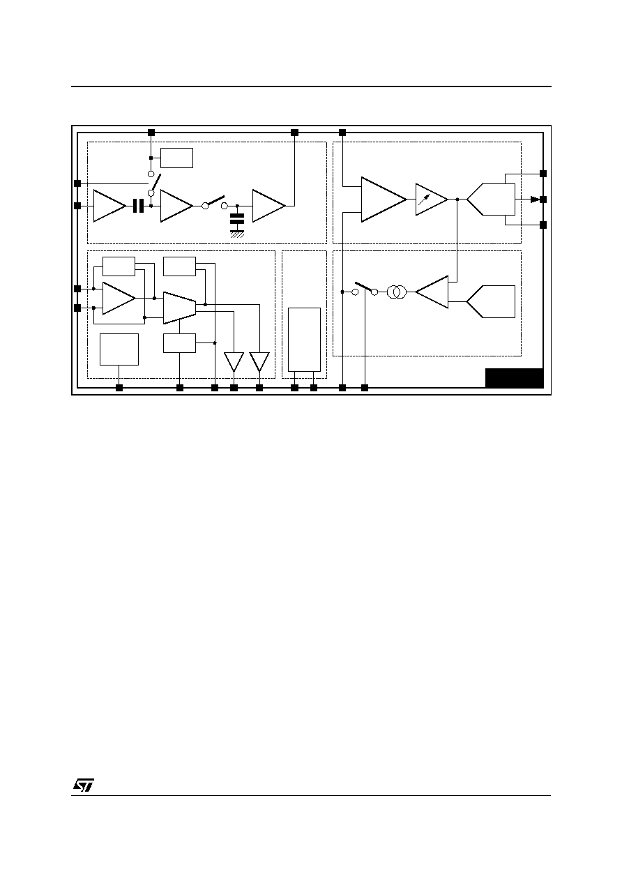
BLOCK DIAGRAM
FUNCTIONAL DESCRIPTION
1 - Video Section
A CCD signal is provided to the STV0502, via a
coupling capacitor, as well as the pulses FS/FCDS.
The CDS (Correlated Double Sampling) is perform-
ing a clamp of the CCD signal during the FCDS
pulse. The signal obtained is then sampled during
the FS pulse, and held the rest of the period. The
resulting signal is then the difference between the
useful pixel level, and the pixel level corresponding
to no charge which can vary from one pixel to
another. Therefore, the parasitic level offset from
one pixel to another is removed.
This signal is DC coupled to the ACG, amplified by
a var iable gain amplif ier, bus co ntrolled
(0.07dB step), which gain is in the range +6dB to
+23.7dB (17.7dB range). Typically, the amplifier is
controlled in order to keep the signal at an optimum
level (AGC) to be digitized. An extra 12dB can be
added up via a bit of the serial interface. In this case
the gain range becomes +18dB up to + 36dB.
At this point, the signal is clamped to a Black level
during the OB pulse. The black level is 5 bits bus
contr olled, and its r ange corr es ponds to
[0 LSB ; 31 LSB] of the ADC. The black level is
made with a 5 bits DC frequency DAC, using the
same V
BOTTOM
and V
TOP
voltage references than
the ADC for matching purposes. The clamp is made
out of a OB pulse sampled comparator between the
DAC output voltage (Black) and the ADC input
signal. The comparator has a symetrical current
output charging a capacitor. The obtained voltage
is buffered and used as a feedback to the AGC
input stage. This clamp makes sure that ADCin is
matched to the DAC black setting during the OB
pulse, disregarding any offset in the AGC path.
Then the signal is digitized by a fast ADC, clocked
at the pixel rate. The output of the chip is then an
8-bit pixel DATA, ready for digital post-processing.
2 - Audio Section
The chip integrates a high gain audio amplifier, in
order to process low signals coming from a speech
microphone, and provide on its output a line level,
differential audio signal, for digital conversion, or
power amplification. Two modes can be selected :
fixed gain mode or AGC mode. In case of AGC
mode, a peak detection of the signal is performed
in order to regulate the output signal on a defined
level of 1.5V
PP
or 1V
PP
(non-diff). This regulated
level can be chosen at 1.5V
PP
or 1V
PP
thanks to a
pin at respectively ground or supply voltage (a pull-
up resistor to supply is already included on chip),
for compatibility purposes between the 502 and
various back-end chips.
The system includes a Low-Noise fixed amplifier
(26dB), and a bias circuitry at the front.
STV0502
3/15
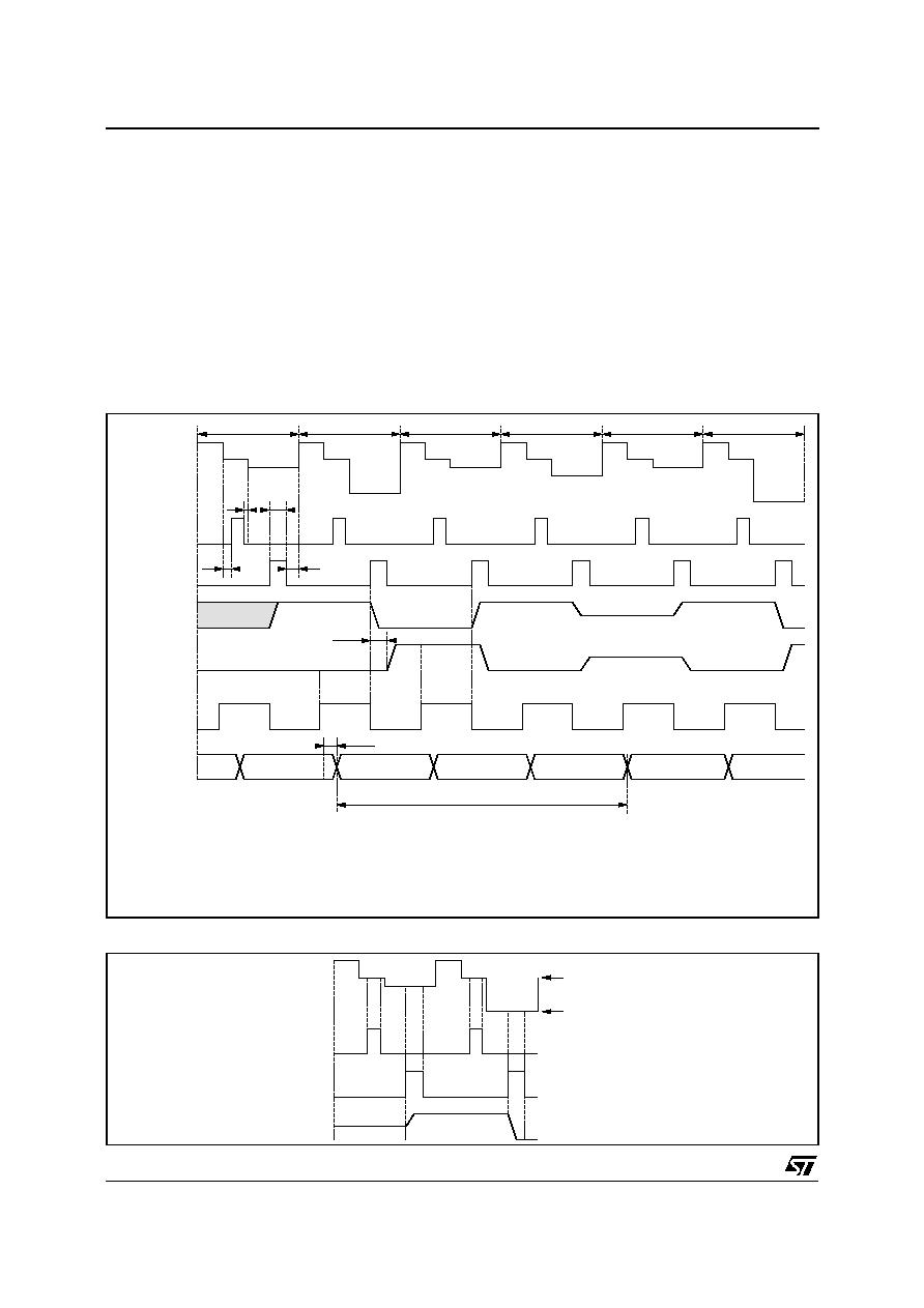
CDS_IN
FCDS
t1
t2
t4
t3
t
PROP
t
DADC
Pixel N
3 CLK Pipe-Line Delay
FS
CDS_OUT
ADC_IN
ADC_CLOCK
DATA_OUT
Sampling
Period
Pixel N+1
Pixel N+2
Pixel N+3
Pixel N+4
Pixel N+5
Pixel N-4
Pixel N-3
Pixel N-2
Pixel N-1
Pixel N
Pixel N+1
Pixel N
Pixel N+1
Pixel N+2
Pixel N+3
Pixel N+4
05
02
-
0
3.
E
P
S
Notation : - t1 is the delay between the falling edge of FCDS and the beginning of the active pixel level from the CCD.
- t2 is the delay between the falling edge of FS and the end of the active pixel level from the CCD.
t1, t2, t3 and t4 must be kept > 0 in the Application.
- t
PROP
is the propagation delay between CDS_OUT and ADC_IN signals (within the AGC block).
- t
DADC
is the delay on the ADC outputs between the rising edge of the clock and data output.
Figure 1
FUNCTIONAL DESCRIPTION (continued)
It is followed by a Voltage Controlled Amplifier
(range 8dB - 34dB), that can be switched into a
fixed 26dB gain amplifier.
The VCA output is differential and 2 buffers are
driving the two output pins, with a load impedance
down to 5k
.
A bias circuitry and an external capacitor (ACC)
form a DC feedback loop on the VCA DC bias, in
order to correct any DC offset on the VCA output.
Finally, a peak detector (double alternance) is used
to compare the output signal with the reference
threshold, to be regulated at. An external capacitor
(CAGC) is used for the AGC time constants. If the
signal goes above the threshold, a 500
�
A current
is charging the capacitor with a fast reponse
time(attack). In case of very big signals, a second
charge cureent of about 5mA is given, in order to
reduce the period during which the output signal is
saturated. Otherwise, a constant 1
�
A current dis-
charges the capacitor with a slow response time
(decay). The capacitor voltage controls the VCA
gain. This constitues the AGC loop.
FS
CDS_OUT
FCDS
CDS_IN =
CCD Signal
Feedtrough Level
Signal Level
0
5
0
2
-0
4
.
EPS
Figure 2
STV0502
4/15
FUNCTIONAL DESCRIPTION (continued)
3 - Serial Bus Specification
It is a 2-wires (data and clock) serial bus, used as
a slave.
Clock line is monodirectional (input) and allways
sent by the master to the chip, whereas Data line
is bidirectional (I/O).
There are 3 registers (8 bits), both writable/readable.
Each register can be addressed by a 4 bits address
word, followed by a R/W bit, and an 8 bits word Data
(read/write).
2 main patterns can be sent : Reset Pattern and
Read/Write pattern.
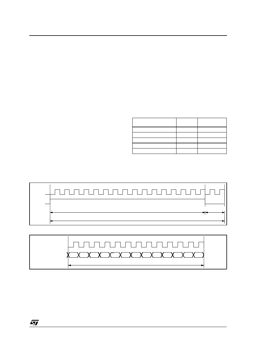
3.1 -Timings and Protocol
The data bit is taken into account when the clock
is rising.
- Reset Pattern : resets all the registers to their
default (Power On) values :
format = 16 * (data=1) | 2 * (data=0)
(total = 18 clocks)
- Read/Write Pattern :
format = 4 addr bits | R/W bit | 8 data bits
(total = 13 clocks)
Please note that :
1/ On power On conditions, SDATA line is in Write
(Input) Mode.
2/ In case of a read pattern, the SDATA line is
automatically set to Read (Output mode) during
8 clock cycles (Data D7 - D0) after R/W bit has
been sent, and comes back in Write (Input
mode) after the 13th clock cycle.
3/ There is no timing restriction between two
consecutive patterns (a pattern being defined
as one of the two above).
3.2 - Register Summary
Register
Address
(A3-A0)
Data Format
(D7-D0)
Video Amplifier Gain
0000
DDDD.DDDD
Black Level Adjust
0001
XXXD.DDDD
Video High Gain Select
0001
XXDX.XXXX
Test Mode
0001
DDXX.XXXX
Microphone AGC
0010
XXXX.XXXD
X
: unused bits
D
: means useful bits
Please note that 3 different functions are merged
in register address 01.
CLK
SDATA
Reset Pattern
1
2
3
4
5
6
7
8
9
10
11
12
13
14
15
16
1
2
2 CLK Cycles
Minimum 16 CLK Cycles
0
5
0
2
-0
5
.
EP
S
Figure 3
CLK
SDATA
Read/Write Pattern
A3
A2
A1
A0
R/W
D7
D6
D5
D4
D3
D2
D1
D0
1
2
3
4
5
6
7
8
9
10
11
12
13
0
5
0
2
-0
6
.
EP
S
Figure 4
STV0502
5/15