 | ÐлекÑÑоннÑй компоненÑ: STV0974E | СкаÑаÑÑ:  PDF PDF  ZIP ZIP |
Äîêóìåíòàöèÿ è îïèñàíèÿ www.docs.chipfind.ru
November 2004
1/69
Rev. 3
STV0974
Features
Supports VS6552 - 640 x 480 (VGA) color
CMOS image sensor
Supports VisionLink low EMI link to image
sensor
Specialized video processor for noise/defect
filtering, color reconstruction, sharpness
enhancement and radial corrections
Programmable gamma correction for LCD
support
Programmable cropping, down-sizing by 1.5,
2, 2.5, 3, 4, 5 and 6, MMS (Multi Media
Messaging Service) digital zoom
JPEG compression, with programmable
target file size
M-JPEG operation at up to 30 frame/s at VGA
resolution
Programmable pixel output format including
ITU-R 656 modes, RGB viewfinder modes and
JPEG baseline
Flashgun control
Flexible host interface:
8-bit data /Hsync /Vsync video output interface
and I²C camera control interface
8-bit microprocessor interface with 2 Kbyte
video FIFO for JPEG data, 10 Kbyte for non-
JPEG data, interrupt and DMA requests
Multi-mode exposure control and color
balance
30 µW ultra low-power standby
6 x 6 mm TFBGA low-footprint & lead-free
package
Description
The STV0974 is a low power digital image
processor designed for the VS6552 color VGA
image sensor. The STV0974 uses advanced image
processing techniques to deliver high quality VGA
images at up to 30 frames per second
(frame/s). The sensor data received via the low EMI
sensor interface is processed in real time: this
includes pixel defect correction, color interpolation,
image sharpness enhancement, selective noise
filtering, cropping and scaling, allowing digital zoom
for ViewFinder or MMS applications. Finally the
image can be JPEG-compressed in real-time. The
STV0974 also performs sensor housekeeping
functions such as automatic exposure and white
balance controls.
Applications
Mobile phone embedded camera system
PDA embedded camera or accessory camera
Wireless security camera
Technical Specifications
Ordering Information
Sensor
640 x 480 color CMOS
(VS6552)
Frame rate (frame/s)
up to 30
Power supply
1.8 +/- 0.1 V
Power requirements
110 mW active
< 30 µW standby
Package dimensions
6 mm x 6 mm x 1.2 mm
Temperature range
[ -25; +70 ] °C
Ordering code
Package
STV0974/TR
TFBGA SnPb balls
STV0974E/TR
TFBGA
AFOP lead-free balls
Mobile Imaging DSP
2/69
STV0974
Contents
Chapter 1
Overview . . . . . . . . . . . . . . . . . . . . . . . . . . . . . . . . . . . . . . . . . . . . . . . . . . . . . . . . .4
1.1
Viewfinder mode . . . . . . . . . . . . . . . . . . . . . . . . . . . . . . . . . . . . . . . . . . . . . . . . . . . . . . . . . 4
1.2
Still features . . . . . . . . . . . . . . . . . . . . . . . . . . . . . . . . . . . . . . . . . . . . . . . . . . . . . . . . . . . . 4
1.3
Live features . . . . . . . . . . . . . . . . . . . . . . . . . . . . . . . . . . . . . . . . . . . . . . . . . . . . . . . . . . . . 4
Chapter 2
Functional block diagram . . . . . . . . . . . . . . . . . . . . . . . . . . . . . . . . . . . . . . . . . . .5
Chapter 3
Signal description . . . . . . . . . . . . . . . . . . . . . . . . . . . . . . . . . . . . . . . . . . . . . . . . .6
Chapter 4
Functional description . . . . . . . . . . . . . . . . . . . . . . . . . . . . . . . . . . . . . . . . . . . . . .7
4.1
Overview . . . . . . . . . . . . . . . . . . . . . . . . . . . . . . . . . . . . . . . . . . . . . . . . . . . . . . . . . . . . . . . 7
4.2
Sensor interface . . . . . . . . . . . . . . . . . . . . . . . . . . . . . . . . . . . . . . . . . . . . . . . . . . . . . . . . . 9
4.3
Video processing unit . . . . . . . . . . . . . . . . . . . . . . . . . . . . . . . . . . . . . . . . . . . . . . . . . . . . 10
4.4
Video compression (VC) . . . . . . . . . . . . . . . . . . . . . . . . . . . . . . . . . . . . . . . . . . . . . . . . . . 13
4.5
Microprocessor interface . . . . . . . . . . . . . . . . . . . . . . . . . . . . . . . . . . . . . . . . . . . . . . . . . . 20
4.6
Video output interface . . . . . . . . . . . . . . . . . . . . . . . . . . . . . . . . . . . . . . . . . . . . . . . . . . . . 28
4.7
Power management unit . . . . . . . . . . . . . . . . . . . . . . . . . . . . . . . . . . . . . . . . . . . . . . . . . . 31
4.8
Clock input . . . . . . . . . . . . . . . . . . . . . . . . . . . . . . . . . . . . . . . . . . . . . . . . . . . . . . . . . . . . 33
4.9
Camera control unit . . . . . . . . . . . . . . . . . . . . . . . . . . . . . . . . . . . . . . . . . . . . . . . . . . . . . . 34
4.10
Additional features . . . . . . . . . . . . . . . . . . . . . . . . . . . . . . . . . . . . . . . . . . . . . . . . . . . . . . 52
Chapter 5
Electrical characteristics . . . . . . . . . . . . . . . . . . . . . . . . . . . . . . . . . . . . . . . . . . .53
5.1
Absolute maximum ratings . . . . . . . . . . . . . . . . . . . . . . . . . . . . . . . . . . . . . . . . . . . . . . . . 53
5.2
Operating conditions . . . . . . . . . . . . . . . . . . . . . . . . . . . . . . . . . . . . . . . . . . . . . . . . . . . . . 53
5.3
Thermal data . . . . . . . . . . . . . . . . . . . . . . . . . . . . . . . . . . . . . . . . . . . . . . . . . . . . . . . . . . . 53
5.4
DC electrical characteristics . . . . . . . . . . . . . . . . . . . . . . . . . . . . . . . . . . . . . . . . . . . . . . . 54
5.5
AC electrical characteristics . . . . . . . . . . . . . . . . . . . . . . . . . . . . . . . . . . . . . . . . . . . . . . . 55
Chapter 6
Package mechanical data . . . . . . . . . . . . . . . . . . . . . . . . . . . . . . . . . . . . . . . . . .61
6.1
Pin assignment . . . . . . . . . . . . . . . . . . . . . . . . . . . . . . . . . . . . . . . . . . . . . . . . . . . . . . . . . 61
6.2
Package dimensions . . . . . . . . . . . . . . . . . . . . . . . . . . . . . . . . . . . . . . . . . . . . . . . . . . . . . 62
Chapter 7
PCB layout guide lines for the STV0974 and VS6552 . . . . . . . . . . . . . . . . . . . .64
STV0974
3/69
Chapter 8
Application schematics . . . . . . . . . . . . . . . . . . . . . . . . . . . . . . . . . . . . . . . . . . . .65
Chapter 9
Evaluation kit and demonstration boards . . . . . . . . . . . . . . . . . . . . . . . . . . . . .67
Revision history . . . . . . . . . . . . . . . . . . . . . . . . . . . . . . . . . . . . . . . . . . . . . . . . . . . . . . . . . . . . . .68
References
. . . . . . . . . . . . . . . . . . . . . . . . . . . . . . . . . . . . . . . . . . . . . . . . . . . . . . . . . . . . . . . .68

4/61
STV0974
Overview
1 Overview
The STV0974 is a mobile imaging digital signal processor which, when used with VS6552 CMOS
color VGA image sensor from STMicroelectronics, performs all the required data processing to
deliver good quality Viewfinder, still and live color images. The STV0974 performs high quality color
processing on images, achieving JPEG compression if requested and transfers them to a
baseband through one of the available interfaces.
Data is transferred from sensor to STV0974 through Low Electromagnetic Interference (EMI)
interface, using the sensor data transfer protocol over LVDS.
Data is transferred from STV0974 to Baseband
through the video output interface. In video mode, the processor streams video data in a format
which closely follows the data format specified in the ITU-R656 standard.
through the microprocessor Interface. In microprocessor mode, the video data is stored in a
small FIFO before is it pulled out of the asynchronous microprocessor interface by the host
system (with DMA support).
1.1 Viewfinder
mode
When connected to microprocessor interface or video output interface, the STV0974 can process
Viewfinder image up to 30 frame/s.
1.2 Still
features
When requested by the baseband, the STV0974 captures bayer data from the sensor. Data is then
color processed, down-scaled and/or compressed and sent through video output or microprocessor
interface. In still mode, the first image produced has a guaranteed good exposure and color
balance for single shot capture.
1.3 Live
features
When connected to microprocessor interface or video output interface, the STV0974 can process
live video up to 30 frame/s and eventually proceed to down-scaling and compression with on-chip
Motion JPEG. Live mode is intended for capture of video sequences.
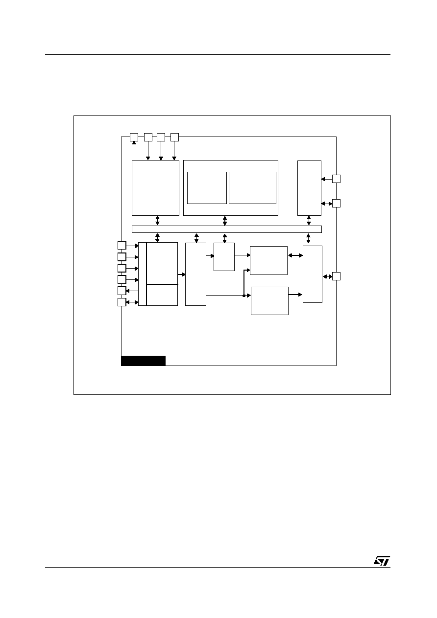
Functional block diagram
STV0974
5/61
2
Functional block diagram
Figure 1: Functional block diagram
MSCL
MSDA
CLK
VP
Parallel
Power
management
Clock &
SCL
SDA
STV0974
RAM - ROM
PDN
DIO[0:13]
POR RST
PCLKP
PCLKN
PDATAP
PDATAN
Mux
I2C
Microprocessor
Internal bus
slave
I2C master
VisionLink
serial
receiver
S
e
n
s
or i
n
t
e
rf
ac
e
FIFO
VC
Video
interface
output
and
interface
Document Outline