 | –≠–ª–µ–∫—Ç—Ä–æ–Ω–Ω—ã–π –∫–æ–º–ø–æ–Ω–µ–Ω—Ç: STV2110B | –°–∫–∞—á–∞—Ç—å:  PDF PDF  ZIP ZIP |
STV2110B
PAL-SECAM LUMA-CHROMA & DEFLECTION PROCESSOR
April 1996
PRELIMINARY DATA
1
2
3
4
5
6
7
8
9
10
11
12
42
41
40
39
38
37
36
35
34
33
32
31
30
29
28
27
26
25
13
14
15
16
17
18
19
20
21
24
23
22
COG
HVcc
BOUT
COB
YIN
SLPF
SXTL
CVBS
LFB
VOUT
HOUT
CTR
DLI
PS
SECIN
SECAM CHROMA INPUT
CHROMA STANDARD I/O
DELAY CHROMA INPUT
CONTRAST CONTROL
HORIZONTAL OUTPUT
VERTICAL OUTPUT
LINE FLYBACK INPUT
COMPOSITE VIDEO SIGNAL
SCANNING LOOP FILTER
SCANNING XTAL
GREEN CUT-OFF CAPACITOR
BLUE OUTPUT
HORIZONTAL Vcc
BLUE CUT-OFF CAPACITOR
LUMINANCE SIGNAL INPUT
Vcc
COR
BRIG
FBL
CLPF
CXTL
CKP
SAT
DLO
CKS
CDR
F440
GND
CDB
F425
GROUND
BLUE DEEMPHASIS CAPACITOR
4.40MHz FILTER
RED DEEMPHASIS CAPACITOR
SECAM KILLER CAPACITOR
CHROMA OUTPUT
SATURATION CONTROL
PAL KILLER CAPACITOR
CHROMA XTAL
SUPPLY VOLTAGE INPUT
RED CUT-OFF CAPACITOR
BRIGHTNESS CONTROL
FAST BLANKING INPUT
CHROMA LOOP FILTER
4.25MHz FILTER
ICAT
CATHODECURRENT
RIN
RED INPUT
BIN
GIN
GREEN INPUT
BLUE INPUT
ACC
ACC CONTROL CAPACITOR
F432
4.32MHz FILTER
GROUND
GND
PALIN
PAL CHROMA INPUT
Vcc
SUPPLY VOLTAGE
BLK
BLANKING INPUT
GOUT
GREEN OUTPUT
ROUT
RED OUTPUT
2110B-01.EPS
PIN CONNECTIONS
SHRINK 42
(Plastic Package)
ORDER CODE : STV2110B
s
RGB AND FAST BLANKING INPUTS
s
AUTOMATIC CUT-OFF CONTROL
s
DC-CONTROLLED BRIGHTNESS, CONTRAST
AND SATURATION
s
CERAMIC 500kHz VCO FOR LINE DEFLEC-
TION
s
CHROMA STANDARD AUTOMATIC IDENTIFI-
CATION
s
BIDIRECTIONAL I/O FOR CHROMA STAND-
ARD
s
PHASE-LOCKED REFERENCE OSCILLATOR
USING A STANDARD 4.43MHz
s
OSD CAPABILITY ON OUTPUTS
s
VIDEO IDENTIFICATION GENERATOR
DESCRIPTION
The STV2110B is a PAL-SECAM chroma decoder,
video and H/V deflection processor for CTV.
Used with the TDA8222, this IC permits a complete
low cost solution with external output stages.
It is pin compatible with STV2102B PAL only proc-
essor.
This is advance information on a new product now in development or undergoing evaluation. Details are subject to change without no tice.
1/15
SAT
35
16
36
Blk.
RGB
5
19
32
34
33
CXTL
CLPF
ACC
CKP
PALIN
SECIN
YIN
9
22
25
20
24
13
12
10
11
15
14
HOUT
VOUT
3
38
8
ROUT
GOUT
BOUT
COR
COG
COB
ICAT
12
7
41
37
39
40
4
6
7
42
2
BLK
30
18
17
31
21
26
29
28
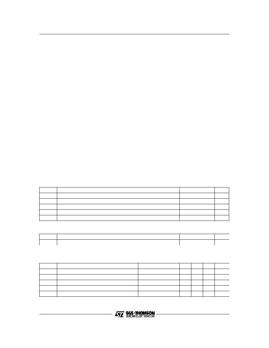
Y
INPUT
CONTRAST
BLACK
INSERTION
CLAMP
BLACK
REFERENCE
MATRIX
SATURATION
CONTRAST
+
CLAMP
RGB
SWITCH
TUBE
TEMP
MEAS.
BRIGHTNESS
BLANKING
RGB
CUT-OFF
LEAK.
CURRENT
MEAS.
LINE
OUTPUT
VCO
DECODER
FRAME
OUTPUT
PHASE
SHIFT
DIVIDER
FRAME
SYNC.
SEPARATOR
LINE
COUNTER
PHASE
COMP.
2
SYNC.
SEPARATOR
BLANKING
COMPENSATION
MUTE
PHASE
COMPARATOR
1
FLIP-FLOP
PAL
FLIP-FLOP
SECAM
BURST
GENERATOR
XVCO
PHASE
DETECTOR
ACC
BURST
DETECTOR
DL
MATRIX
KILLER
PAL
DEMODULATION
≠
90DEG
STANDARD
CONTROL
PERMUTATOR
SECAM
DEMODULATION
SECAM
IDENTIFICATION
GND
GND
DL O
DL I
PS
CKS
23
F42
5
CDB
F43
2
CDR
F44
0
CV BS
LFB
SLP
F
SXTL
BRIG
CTR
BIN
GIN
RIN
FBL
SAT
HV
CC
V
CC
V
CC
STV2110B
2110B-02.EPS
BLOCK DIAGRAM
STV2110B
2/15

FUNCTIONAL DESCRIPTION
DEFLECTION
Synchronization Separator
The synchronization separator is based on the
bottom of synchronization pulses alignment to an
internal reference voltage. An external capacitor
permits to align synchro. pulses, two external resis-
tors determines the detection threshold of synchro
pulses. The frame synchronization pulses are
locked to a 32
µ
s reference signal to perfect inter-
lacing.
Horizontal Scanning
The horizontal scanning frequencyis obtained from
a 500kHz VCO. The circuit uses two phase-locked
loops (PLL). The first one controls the frequency;
the second one, fully integrated, controls the rela-
tive phase of the synchronization and the line fly-
back signals.
The first PLL has two times constants : a long time
constant during the picture to have a good noise
immunity, a short time constant at the beginning of
the frame to recapture faster the phase in case of
VCR video signal. More over, the PLL is in short
time constant three lines before frame pulses oc-
cured, it permits to ensure good interlacing when
the video signal comes from a VCR tape with high
phase error.
The horizontal output signal is 28
µ
s width. On
starting up, horizontal pulses are enabled at
V
CC
= 6.8V. On shutting down, horizontal pulses
are inhibited for V
CC
= 6.2V.
Vertical Scanning
The windows for the frame sync detection are
generated by a count down system. The selection
of the windows is determined by the IC status :
- video identification off - window : 248/314
- video identification on - window : 248/352
When a sync pulse is detected inside the window
a 10.5 lines long pulse is provided to V
OUT
pin.
The count down system provides also the needed
signals for the time constant switch, the line PLL
inhibition and service signals to the rest of the IC.
CHROMA
ACC Amplifier, DL Matrix, Permutator and De-
modulator
The correct chroma subcarrier input, issued from
bandpass or bell filter, is internally selected with the
standard. The ACC amplifier envolves th ree
stages : the first one select the correct input, the
second one the -6dB in picture (PAL mode), the
third one is controled by the ACC voltage.
The dynamic range is over than 30dB.
The chrominance output signal is fed to the delay
line.
- PAL mode :
the adding and substracting direct and delayed
signals are performed by the DL matrix function.
Two synchronous demodulators multiplies
the (B-Y) signal with the 0 degree phase
4.43MHz reference signal and the (R-Y) signal
with the alternate
±
90 deg. 4.43MHz phase ref-
erence signal.
- SECAM mode :
the permutator separates the two (B-Y) and (R-Y)
subcarriers. These signals are demodulated by
two FM demodulators with two external L, C
centered on f
O(blue)
= 4.25MHz and f
O(red)
=
4.406MHz.
4.43MHz Phase Locked Loop
The oscillating frequency of the 4.43MHz crystal
oscillator is controlled by the output voltage of the
loop filter. The phase detector will lock the 90 de-
gree reference signal to the direct burst signal.
A 90 degree phase shifter permits to recover the
0 degree reference signal. A flip-flop driven by line
pulses permits to generate the alternate
±
90 de-
gree signal.
ACC Control and Color Killer
PAL mode :
the direct burst signal is demodulated with the
±
90
degree reference signal. The demodulation result
is used by ACC control and killer function.
SECAM mode :
ACC control is done by a X
2
demodulator. For
identification the burst signals of the red and blue
lines are demodulated by the external LC con-
nected on Pin 31, it is centered at 4.32MHz. This
give positive and negative signals which are in-
verted by the signal coming out of the SECAM
flip-flop.
In both standard, if the demodulation result is al-
ways positive, the killer capacitor is charged and
the standard is identified (color ON). When de-
modulation result is always negative, the killer ca-
pacitor voltage reaches the flip-flop inhibition level,
so the alternace sequence is reversed and the
capacitor is charged again.
In case of no video signal, both killer capacitors
voltage are maintained about V
CC
/2, below the
color off threshold.
In PAL or SECAM, the ACC control voltage is
obtained by the peak detection of the demodulated
burst.
STV2110B
3/15
Automatic Standard Identification
The circuit is alternatelyforced in each mode during
two fields (PAL mode, SECAM mode disabled or
SECAM mode, PAL mode disabled).
If PALsignal is identified, the alternate PAL/SECAM
sequency is locked in PAL mode.
To have a SECAM identification, the circuit must
memorizes a first SECAM identification, than test
the PAL mode and confirm a second SECAM iden-
tification. The SECAM identification will take from
four to six fields.
Output Pin 21, named PS, is high level in PAL mode
and low level in SECAM mode.
Forced standard : Pin 21 can be used for the
purpose :
- Pin 21 to HVCC : PAL mode
- Pin 21 to ground : SECAM mode
VIDEO
Input Stage
The luminance input is controlled by the contrast
control stage which range is 20dB.
The luminance and color difference signals are
added in the video matrix circuit to obtain the color
signals.
The color signals are sent to an RGB switch which
will drive to the outputs either internal RGB signals
or external RGB signals.
Automatic Cut-off Control
The black levels of the RGB outputs are controlled
with the cut-off loops during three line periods after
the frame retrace. The cut-off measurements are
sequentially achieved during these three lines. The
leakage current measurement is achieved during
the frame retrace and memorized on an internal
capacitor, thus the circuit is able to extract the
cut-off current from the total current measurement.
Warm-up Detector
At the start-up, the cut-off loops are switch off, a
white level is inserted on the luminance signal until
a cathode current is detected. Then the cut-off
loops are released.
RGB Inputs
To avoid the black level of the inserted signal
differing from the black level of the normal video
signal, the external RGB are clamped to the black
level of the luminance signal. Therefore, an AC
coupling is required for the RGB inputs.
The RGB inputs are controlled by a 12dB range
contrast control stage.
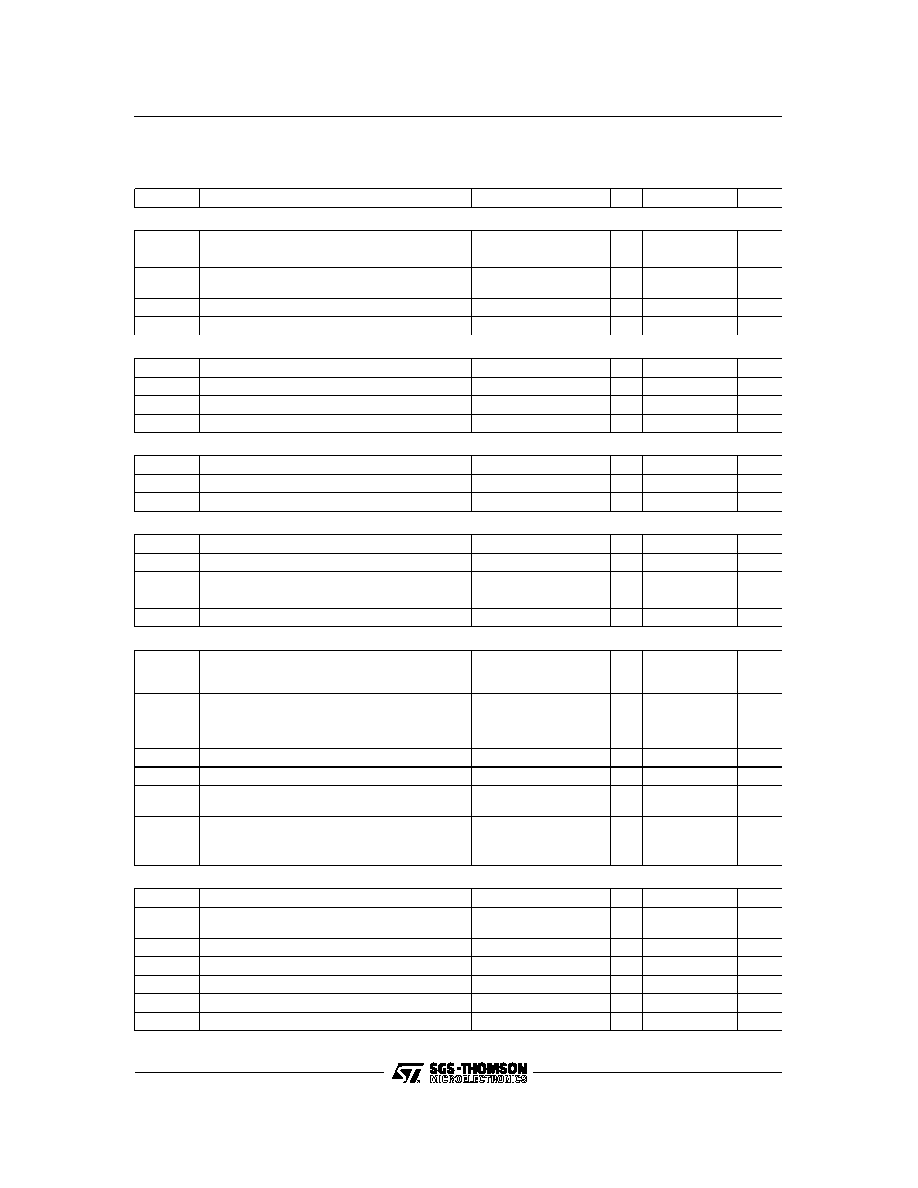
ABSOLUTE MAXIMUM RATINGS
Symbol
Parameter
Value
Unit
HV
cc
Horizontal Supply Voltage (Pin 5)
12
V
V
cc
Video & Chroma Supply Voltage (Pins 1-41)
HV
CC
+ 0.5
V
H
OUT
Horizontal Output (Pin 15)
12
V
T
stg
Storage Temperature
-55, +150
o
C
T
oper
Operating Temperature
0, +70
o
C
2110B-01.TBL
THERMAL DATA
Symbol
Parameter
Value
Unit
R
th (j-a)
Junction-ambient Thermal Resistance
Max.
60
o
C/W
2110B-02.TBL
DC AND AC ELECTRICAL CHARACTERISTICS
(HV
CC
= V
CC
= 9V, T
amb
= 25
o
C unless otherwise specified)
Symbol
Parameter
Test Conditions
Min.
Typ.
Max.
Unit
HV
cc
Scanning Supply Voltage (Pin 5)
8.1
9
9.9
V
V
cc
Video & Chroma Supply Voltage (Pins 1-41)
8.1
9
9.9
V
I
cch
Scanning Supply Current (pin 5)
No load
25
35
mA
I
ccv&c
Video & Chroma Supply Current (Pins 1-41)
No load
45
55
mA
P
D
Total Power Dissipation
No load
630
890
mW
2110B-03.TBL
FUNCTIONAL DESCRIPTION (continued)
STV2110B
4/15
DC AND AC ELECTRICAL CHARACTERISTICS (continued)
(HV
CC
= V
CC
= 9V, T
amb
= 25
o
C unless otherwise specified)
Symbol
Parameter
Test Conditions
Min.
Typ.
Max.
Unit
LUMINANCE INPUT (Pin 9)
V
BW9
Input Voltage
350
490
mV
PP
V
DC9
DC Level
No input signal
2.6
V
I
g
Input Current
∑
During burst period
∑
Out of burst period
±
150
1
µ
A
µ
A
G
9
Luma Gain
7.4
BW467
Bandwidth (Y to R, G, B outputs)
-3dB
6
MHz
CONTRAST CONTROL (Pin 16)
V
16
Contrast Control Voltage
2 to 4
V
V
16 (Max.)
Allowed Control Voltage
5
V
G
16
Contrast Control Range
20
dB
I
16
Input Current
10
µ
A
BRIGHTNESS CONTROL (Pin 36)
V
36
Brightness Control Voltage
1.8 to 4.3
V
V
36 (Max.)
Allowed Control Voltage
5
V
I
36
Input Current
10
µ
A
SATURATION CONTROL INPUT (Pin 27)
V
27
Saturation Control Voltage
2 to 4
V
V
27 (Max.)
Allowed Control Voltage
5
V
G
27
Saturation Control Range
-50
dB
V
27M
Mute Level
0.5
V
I
27
Input Current
10
µ
A
RGB OUTPUTS (Pins 4-6-7)
V
BW 4-6-7
Output Signal Amplitude
(black to white)
∑
0.35V B to W @ Pin 9
∑
Contrast @ 4V
∑
Sat. & Brig. @ 3V
2.6
V
I
4-6-7
Individual Output Sinking Current
2
mA
VM
4-6-7
Maximum Peak White Level
7.8
V
V
blank 4-6-7
Blanking Level
0.5
V
V
CO min.
Minimum Level of Inserted Cut-off Lines
2.5
V
V
CO max.
Maximum Level of Inserted Cut-off Lines
4.5
V
Relative Variation in Black Level with Various
CONT. SAT. BRIG between the 3 channels
20
mV
V
temp
Black Level Thermal Drift
0.5
mV/
o
C
Tracking between Luminance and Chrominance
Signals over 10dB Contrast Control
2
dB
RGB INPUTS (Pins 37-39-40)
V
BW37-39-40
Input Amplitude (B to W)
0.7
2
V
V
clamp
37-39-40
Clamp Level
Contrast max
1.8
V
I
37-39-40
Control Current
±
150
µ
A
I
i37-39-40
Leakage Current
1
µ
A
BW
37-39-40
Bandwidth
-3dB
8
MHz
G
CTR
RGB Contrast Control Range
14
dB
G
37-39-40
RGB Gain
3.7
2110B-04.TBL
STV2110B
5/15