 | –≠–ª–µ–∫—Ç—Ä–æ–Ω–Ω—ã–π –∫–æ–º–ø–æ–Ω–µ–Ω—Ç: STV2247 | –°–∫–∞—á–∞—Ç—å:  PDF PDF  ZIP ZIP |
September 2003
1/76
STV223XD/224XC
I≤C BUS-CONTROLLED MULTISTANDARD
SINGLE CHIP TV PROCESSOR
s
I≤C Bus Control
s
PIF Circuit with PLL Demodulation
(Positive and Negative Video)
s
SIF Circuit with QSS Structure, FM
Demodulation and AM Demodulation for France
s
Intercarrier Capability
s
Built-in Sound Bandpass
s
Sound Subcarrier Output for Stereo Chassis
(FM, NICAM)
s
Audio Switch and Volume Control (Mono
Chassis)
s
AVL (Automatic Volume Levelling)
s
Integrated Chroma Filters and Luma Delay Line
s
Integrated Chroma Delay Line
s
Video Switch (3 CVBS In, 1 or 2 CVBS Out)
s
SVHS Switch (Y Combined with CVBS3 Input)
s
OSD RGB Inputs
s
External RGB/YCrCb Inputs or YUV Interface
s
PAL / SECAM / NTSC Chroma Demodulators
s
Auto Flesh Control Capability in NTSC mode
s
South America Capability (PAL-M / PAL-N /
NTSC)
s
Chroma Subcarrier Output
s
Black Stretch Circuit
s
Peaking Circuit
s
Automatic Cut-off Current Loop
s
Manual Cut-off possible for low-cost
applications
s
Two Horizontal Deflection PLLs
s
Vertical Countdown
s
Half Contrast
s
APR (Automatic RGB Peak Regulation)
Function
s
SAW Filter Switch Control (Optional)
s
Very Few External Components
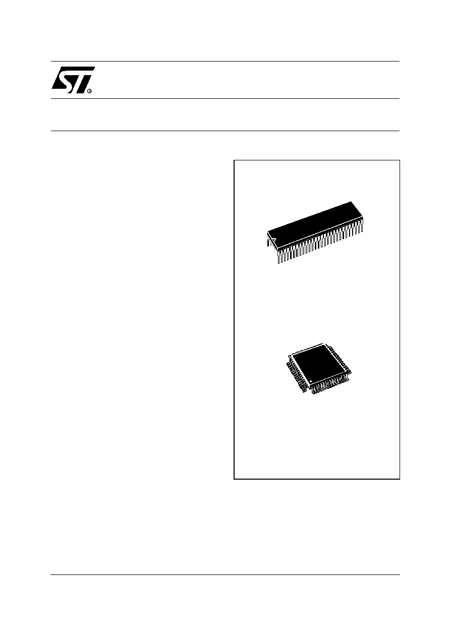
TQFP64 (14 x 14 x 1.4 mm)
(Full Thin Plastic Quad Flat Pack)
ORDER CODE: STV223XD
SHRINK56
(Plastic Package)
ORDER CODE: STV224XC/8XC
1

Table of Contents
76
2/76
1 GENERAL DESCRIPTION . . . . . . . . . . . . . . . . . . . . . . . . . . . . . . . . . . . . . . . . . . . . . . . . . . . . . . 3
1.1 INTRODUCTION . . . . . . . . . . . . . . . . . . . . . . . . . . . . . . . . . . . . . . . . . . . . . . . . . . . . . . . . . 3
1.2 PIN DESCRIPTION . . . . . . . . . . . . . . . . . . . . . . . . . . . . . . . . . . . . . . . . . . . . . . . . . . . . . . . 4
2 STV2238D MAIN FEATURES . . . . . . . . . . . . . . . . . . . . . . . . . . . . . . . . . . . . . . . . . . . . . . . . . . . 16
3 FUNCTIONAL DESCRIPTION . . . . . . . . . . . . . . . . . . . . . . . . . . . . . . . . . . . . . . . . . . . . . . . . . . 17
3.1 DETAILED FEATURES . . . . . . . . . . . . . . . . . . . . . . . . . . . . . . . . . . . . . . . . . . . . . . . . . . . 17
3.1.1 Power Supplies . . . . . . . . . . . . . . . . . . . . . . . . . . . . . . . . . . . . . . . . . . . . . . . . . . . . 17
3.1.2 Picture Intermediate Frequency (PIF) . . . . . . . . . . . . . . . . . . . . . . . . . . . . . . . . . . . 17
3.1.3 Sound Intermediate Frequency (SIF) and Sound Demodulators . . . . . . . . . . . . . . . 17
3.1.4 Audio Switch . . . . . . . . . . . . . . . . . . . . . . . . . . . . . . . . . . . . . . . . . . . . . . . . . . . . . . 17
3.1.5 Surface Acoustic Wave (SAW) Filter Switch Control . . . . . . . . . . . . . . . . . . . . . . . . 17
3.1.6 Video Switches . . . . . . . . . . . . . . . . . . . . . . . . . . . . . . . . . . . . . . . . . . . . . . . . . . . . 17
3.2 DEFLECTION PART . . . . . . . . . . . . . . . . . . . . . . . . . . . . . . . . . . . . . . . . . . . . . . . . . . . . . 1 8
3.3 FILTERS . . . . . . . . . . . . . . . . . . . . . . . . . . . . . . . . . . . . . . . . . . . . . . . . . . . . . . . . . . . . . . 19
3.4 VIDEO CIRCUIT . . . . . . . . . . . . . . . . . . . . . . . . . . . . . . . . . . . . . . . . . . . . . . . . . . . . . . . . 20
3.5 CHROMA CIRCUIT . . . . . . . . . . . . . . . . . . . . . . . . . . . . . . . . . . . . . . . . . . . . . . . . . . . . . . 21
3.6 CHROMA STANDARD IDENTIFICATION . . . . . . . . . . . . . . . . . . . . . . . . . . . . . . . . . . . . . 21
4 ELECTRICAL CHARACTERISTICS . . . . . . . . . . . . . . . . . . . . . . . . . . . . . . . . . . . . . . . . . . . . . . 22
4.1 ABSOLUTE MAXIMUM RATINGS . . . . . . . . . . . . . . . . . . . . . . . . . . . . . . . . . . . . . . . . . . . 22
4.2 THERMAL DATA . . . . . . . . . . . . . . . . . . . . . . . . . . . . . . . . . . . . . . . . . . . . . . . . . . . . . . . . 22
4.3 SUPPLY . . . . . . . . . . . . . . . . . . . . . . . . . . . . . . . . . . . . . . . . . . . . . . . . . . . . . . . . . . . . . . . 22
4.4 IF SECTION . . . . . . . . . . . . . . . . . . . . . . . . . . . . . . . . . . . . . . . . . . . . . . . . . . . . . . . . . . . . 23
4.5 CVBS, Y/C, RGB INPUTS AND CVBS OUTPUTS . . . . . . . . . . . . . . . . . . . . . . . . . . . . . . 27
4.6 LUMA PART . . . . . . . . . . . . . . . . . . . . . . . . . . . . . . . . . . . . . . . . . . . . . . . . . . . . . . . . . . . . 30
4.7 FILTERS . . . . . . . . . . . . . . . . . . . . . . . . . . . . . . . . . . . . . . . . . . . . . . . . . . . . . . . . . . . . . . 31
4.8 CHROMA PART . . . . . . . . . . . . . . . . . . . . . . . . . . . . . . . . . . . . . . . . . . . . . . . . . . . . . . . . . 31
4.9 SCANNING PART . . . . . . . . . . . . . . . . . . . . . . . . . . . . . . . . . . . . . . . . . . . . . . . . . . . . . . . 33
4.10 RGB CONTROL PART . . . . . . . . . . . . . . . . . . . . . . . . . . . . . . . . . . . . . . . . . . . . . . . . . . . 35
4.11 I≤C BUS CHARACTERISTICS . . . . . . . . . . . . . . . . . . . . . . . . . . . . . . . . . . . . . . . . . . . . . . 39
5 I≤C BUS SPECIFICATIONS . . . . . . . . . . . . . . . . . . . . . . . . . . . . . . . . . . . . . . . . . . . . . . . . . . . . 40
6 I≤C BUS SELECTION . . . . . . . . . . . . . . . . . . . . . . . . . . . . . . . . . . . . . . . . . . . . . . . . . . . . . . . . . 41
6.1 STV2238D: SUMMARY INPUT SIGNALS (WRITE MODE) . . . . . . . . . . . . . . . . . . . . . . . 41
6.2 STV2238D: SUMMARY OUTPUT SIGNALS (READ MODE) . . . . . . . . . . . . . . . . . . . . . . 42
6.3 STV2238D: INPUT SIGNALS (WRITE MODE) . . . . . . . . . . . . . . . . . . . . . . . . . . . . . . . . . 43
6.4 OUTPUT SIGNALS (READ MODE) . . . . . . . . . . . . . . . . . . . . . . . . . . . . . . . . . . . . . . . . . . 49
6.5 POWER-ON RESET - INITIAL BUS REGISTER CONDITIONS . . . . . . . . . . . . . . . . . . . . 51
7 I≤C BUS SPECIFICATION COMPATIBILITY . . . . . . . . . . . . . . . . . . . . . . . . . . . . . . . . . . . . . . . 52
8 INPUT/OUTPUT SCHEMATIC DIAGRAMS . . . . . . . . . . . . . . . . . . . . . . . . . . . . . . . . . . . . . . . . 53
9 APPLICATION DIAGRAMS . . . . . . . . . . . . . . . . . . . . . . . . . . . . . . . . . . . . . . . . . . . . . . . . . . . . 70
10 SUMMARY OF CHANGES . . . . . . . . . . . . . . . . . . . . . . . . . . . . . . . . . . . . . . . . . . . . . . . . . . . . 74
11 GENERAL PACKAGE INFORMATION . . . . . . . . . . . . . . . . . . . . . . . . . . . . . . . . . . . . . . . . . . 75
11.1 PACKAGE MECHANICAL DATA . . . . . . . . . . . . . . . . . . . . . . . . . . . . . . . . . . . . . . . . . . . . 75
1
STV223XD/224XC - GENERAL DESCRIPTION
3/76
1 GENERAL DESCRIPTION
1.1 INTRODUCTION
The STV223XD/224X are fully bus-controlled ICs
for TV that include PIF, SIF, Luma, Chroma and
Deflection processing functions. Used with a verti-
cal frame booster (TDA8174A for a 90∞ chassis,
STV9306 for a 110∞ chassis), they allow multistan-
dard (BGDKIMNLL', PAL/SECAM/NTSC) sets to
be designed with very few external components
and no manual adjustments.
STV22XX Family Characteristics
Package
Application
PAL/NTSC
Intercarrier
PAL/NTSC
QSS/Intercarrier
PAL/SECAM/NTSC
QSS/Intercarrier
AM
PAL/SECAM/NTSC
QSS/Intercarrier
SHRINK56
STV2246C/86C
STV2247C
STV2248C
STV2249C
TQFP64
STV2236D
STV2237D
STV2238D
STV2239D
STV22XX IC Versions
Function
IC Version
SHRINK56
TQFP64
2246C 2247C 2248C 2249C 2286C 2236D 2237D 2238D 2239D
PAL/SECAM/NTSC
X
X
X
X
PAL/NTSC
X
X
X
X
X
QSS/Intercarrier
X
X
X
X
X
X
Intercarrier Only
X
X
X
AM
X
X
2 CVBS Outputs
X
X
X
X
X
X
X
X
X
1 EXT RGB Input (OSD)
X
OSD RGB Inputs & RGBEXT/YCrCb Inputs
X
X
X
X
X
X
X
X
YUV Interface
X
X
X
APR
X
X
X
X
X
X
X
X
X
Half Contrast
X
X
X
X
X
X
X
X
X
SAW Filter Control
X
X
X
X
1
STV223XD/224XC - GENERAL DESCRIPTION
4/76
1.2 PIN DESCRIPTION
Table 1. Pin Configuration
Pin N∞
Symbol
Description
STV224XC/8XC
STV223XD
SDIP56
TQFP64
1
8
SIFIN1
SIF Input (Please refer to Note 1)
2
9
SIFIN2
SIF Input (Please refer to Note 1)
3
10
AGCSIFCAP
AGC SIF Capacitor (Please refer to Note 1)
4
11
V
REFIF
Voltage Reference Filtering
5
12
AGCPIFCAP
AGC PIF Capacitor
6
13
PIFIN1
PIF Input
7
14
PIFIN2
PIF Input
8
16
TUNERAGCOUT
AGC Tuner Output
9
17
IFPLL
IF PLL Filter
10
18
GND
IF
IF Ground
11
19
AM/FMOUT/SC
AM/FM Mono Sound or Stereo Carriers Output
12
20
V
CCIF
5 V IF Supply
13
21
INTCVBSOUT
Internal CVBS Output
14
22
EXTAUDIOIN
External Audio Input
15
23
PIFLC1
LC Input
16
24
PIFLC2
LC Input
17
25
V
CC2
Video/Luma Supply Voltage (8 V)
18
26
CVBSIN1
Internal Video Input
19
27
GND2
Video/Luma Ground
20
28
CVBSIN2
External Video Input
21
29
BS
Black Stretch Capacitor
22
34
Y/CVBSIN3
Y(SVHS) or CVBS3 External Input
23
35
CHR
Chroma (SVHS) Input
-
37
UIN
B-Y Input (Please refer to Note 1)
-
38
VIN
R-Y Input (Please refer to Note 1)
-
39
YIN
Y Input (Please refer to Note 1)
-
40
YOUT
Y Output (Please refer to Note 1)
-
41
VOUT
R-Y Output (Please refer to Note 1)
-
42
UOUT
B-Y Output (Please refer to Note 1)
30
43
BOUT
Blue Output
31
44
GOUT
Green Output
32
45
ROUT
Red Output
33
46
I
CATH
Cathode Current Measurement Input
34
47
BOSD
OSD Blue Input
35
48
GOSD
OSD Green Input
36
49
ROSD
OSD Red Input
37
50
FBOSD/HC
OSD Fast Blanking Input / Half Contrast on SDIP56 package
38
52
XTAL3/BTUN
3.5X MHz Crystal or Cloche Filter Tuning Capacitor
39
53
XTAL2
3.5X MHz Crystal
40
54
XTAL1
4.43/3.5X MHz Crystal
41
55
CLPF
Chroma PLL Filter
42
56
X1/VAMP/CHROUT
XTAL1 Control Pin, Vertical Amplitude DAC Output and
Chroma Reference Signal Output
1
STV223XD/224XC - GENERAL DESCRIPTION
5/76
Note 1: Input/Output not available in STV2246C/86C and STV2236D versions. This pin must not be con-
nected.
Note 2: When REXT, GEXT and BEXT pins are not used, they must not be connected. Register 0Ah must
be set (d7 and d6 = 01). (RGB external inputs disabled.)
Note 3: FBEXT to be connected to ground when not used.
Note 4: CVBS output 1 on pin 29 (SDIP56), if register 1Dh = 07h.
43
57
GND1
Chroma/Scanning Ground
-
58
CVBSOUT1
Main Video Switch Output
45
59
V
CC1
Chroma/Scanning Power Supply (8 V)
46
61
BCL/SAF
Beam Current Limiter Control Voltage and Safety Input
(XRAY)
47
62
VERT
Vertical Output Pulse
48
63
HOUT
Horizontal Output Pulse
49
64
LFB/SSC
Line Flyback Input and Super-Sandcastle Output
50
1
SLPF
Scanning PLL Filter
51
2
SCL
I≤C Bus Clock Input
52
3
SDA
I≤C Bus Data Input
53
4
V
CCD
Digital Supply Voltage (5 V)
54
5
GNDD
Digital Ground
55
6
AUDIOOUT
Main Audio Output
56
7
FMCAP
FM Demodulation Capacitor
-
15
SAW
Filter Switch Control
25
30
BEXT/Cb
External Blue Input or external Cb Input
(Please refer to Note 2)
26
31
GEXT/Y
External Green Input or external Y Input
(Please refer to Note 2)
27
32
REXT/Cr
External Red Input or external Cr Input
(Please refer to Note 2)
28
33
FBEXT
External Fast Blanking Input (Please refer to Note 3)
24
36
APR
Automatic RGB Peak Regulation
-
51
HC
Half Contrast Input
44
60
CVBSOUT2
Second Video Switch Output
29
-
NTBC/CVBSOUT1
Not To Be Connected or CVBS Output 1
(Please refer to Note 4)
Pin N∞
Symbol
Description
STV224XC/8XC
STV223XD
SDIP56
TQFP64
STV223XD/224XC - GENERAL DESCRIPTION
6/76
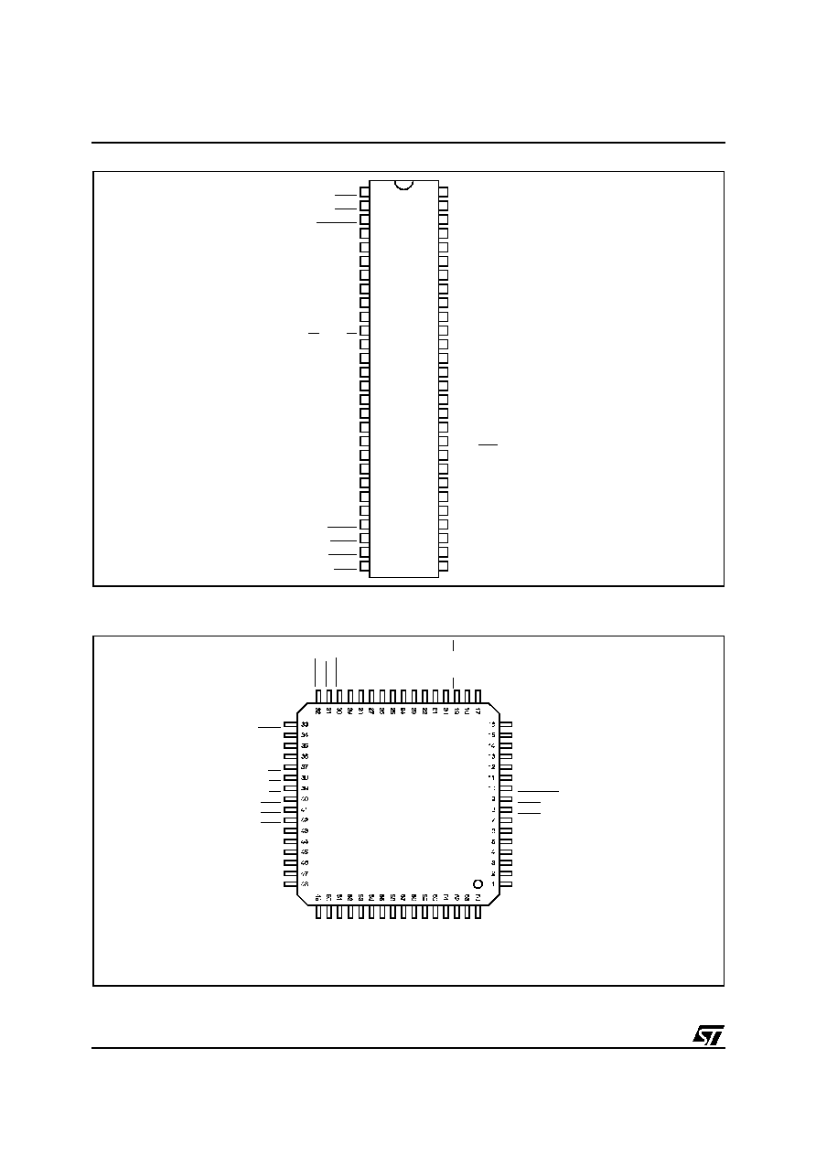
Figure 1. STV224XC/8XC Pinout (SDIP56)
Note: Underlined pin functions are optional.
Figure 2. STV223XD Pinout (TQFP64)
SIFIN1
SIFIN2
AGCSIFCAP
V
REFIF
AGCPIFCAP
PIFIN1
PIFIN2
TUNERAGCOUT
IFPLL
GND
IF
AM/FMOUT/SC
V
CCIF
INTCVBSOUT
EXTAUDIOIN
PIFLC1
PIFLC2
V
CC2
CVBSIN1
GND2
CVBSIN2
BS
Y/CVBSIN3
CHR
APR
BEXT/Cb
GEXT/Y
REXT/Cr
FBEXT
FMCAP
AUDIOOUT
GNDD
V
CCD
SDA
SCL
SLPF
LFB/SSC
HOUT
VERT
BCL/SAF
V
CC1
CVBSOUT2
GND1
X1/VAMP/CHROUT
CLPF
XTAL1
XTAL2
XTAL3/BTUN
ROSD
GOSD
BOSD
I
CATH
ROUT
GOUT
BOUT
NTBC/CVBSOUT1
FBOSD/HC
1
2
3
4
5
6
7
8
9
10
11
12
13
14
15
16
17
18
19
20
21
22
23
24
25
26
27
28
56
55
54
53
52
51
50
49
48
47
46
45
44
43
42
41
40
39
38
37
36
35
34
33
32
31
30
29
TUNERAGCOUT
SAW
PIFIN2
PIFIN1
AGCPIFCAP
V
REFIF
AGCSIFCAP
SIFIN2
SIFIN1
FMCAP
AUDIOOUT
GNDD
V
CCD
SDA
SCL
SLPF
LF
B
/
S
S
C
HO
UT
VE
R
T
B
C
L
/
SAF
CV
BSO
UT
2
V
CC1
CV
BSO
UT
1
G
ND1
X
1
/
VAM
P/
CHRO
UT
CL
PF
XT
A
L
1
XT
A
L
2
X
T
AL
3
/
BT
UN
HC
FB
O
S
D
RO
SD
FBEXT
Y/CVBSIN3
CHR
APR
UIN
VIN
YIN
YOUT
VOUT
UOUT
BOUT
GOUT
ROUT
I
CATH
BOSD
GOSD
IF
PL
L
GN
D
IF
AM
/F
M
O
U
T
/
S
C
V
CCI
F
I
N
T
C
VB
SO
UT
EXT
A
U
D
I
O
I
N
PI
F
L
C1
PI
F
L
C2
V
CC2
CVBSI
N1
G
ND2
CVBSI
N2
BS
BEXT
/
C
b
G
EXT
/
Y
REXT
/
C
r
STV223XD/224XC - GENERAL DESCRIPTION
7/76
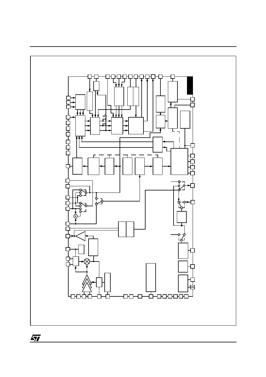
Figure 3. STV2236D (TQFP64) Block Diagram
ST
V2
2
3
6
D
FB
O
S
D
RO
S
D
GO
S
D
BO
S
D
BC
L
/
SA
F
I
CAT
H
RO
UT
GO
U
T
BO
U
T
VE
R
T
HO
UT
BC
L/
SAF
BR
IG
H
T
.
DR
I
V
E
CU
T
-
O
F
F
B
L
AN
KI
N
G
LFB/SSC
BA
N
D
PA
S
S
FI
L
T
E
R
AC
C
&
AC
C
OV
ER
L
O
A
D
LU
M
A
D
L
PEA
KIN
G
&
CO
RI
NG
FBEXT
RG
B
TO
Y
U
V
I
≤C
B
U
S
DE
CO
DE
R
FM
M
o
n
o
GN
D
D
V
REFIF
HC
AP
R
HO
RIZ
O
NT
A
L
2nd LO
O
P
HO
RIZ
O
NT
A
L
1s
t LO
O
P
A
U
TO
I
D
E
N
T.
K
I
LLE
R
PA
L
/
N
T
S
C
DE
M
O
DUL
A
T
O
R
VE
R
T
I
C
A
L
S
C
A
NNING
S
Y
NC.
SE
P
CHR
O
M
A
DL
VAM
P D
C
CO
N
T
RO
L
A
UDI
O
RE
F
BL
AC
K
ST
R
E
T
C
H
CH
RO
M
A
TR
A
P
FI
L
T
E
R
T
U
NI
NG
AG
C
T
UNE
R A
G
C
S
O
UND B
P
FM D
E
M
O
D
Mu
t
e
Mu
t
e
S
A
T
./C
ON
T
MA
T
R
I
X
10
NTB
C
15
SAW
V
CCI
F
18
GN
D
IF
20
59
V
CC1
57
GN
D
1
V
CC2
27
G
ND2
25
PL
L
23
PIFLC1
24
PIFLC2
I
CAT
H
SEN
S
E
AF
C
SAW
F
I
L
T
ER
S
W
I
T
CH CO
NTR
O
L
17
IFPLL
35
CHR
34
Y/CVBSIN3
28
CVBSIN2
26
CVBSIN1
58
CVBSOUT1
60
CVBSOUT2
7
FMCAP
21
INTCVBSOUT
D
EEM
P.
HA
L
F
C
T
R
APR
SLPF
X1/VAMP/CHROUT
CLPF
XTAL1
XTAL2
XTAL3
FMOUT
EXTAUDIOIN
AUDIOOUT
VO
L
U
M
E
RG
B
SW
IT
C
H
YU
V
SW
IT
C
H
NTBC
NTBC
NTBC
NTBC
NTBC
NTBC
38
37
39
41
42
40
3
3
51
36
50
49
48
47
46
45
43
62
63
44
61
RG
B
CO
NTR
A
S
T
64
55
56
52
53
54
19
22
SCL
SDA
2
6
11
NT
B
C
NTB
C
9
8
W/
B
S
P
O
T
IN
VER
T
E
R
4
5
13
14
12
16
V
CCD
PI
F
I
N
1
PI
F
I
N
2
AG
C
P
IF
C
A
P
T
U
N
E
R
A
GOU
T
30
BEXT/Cb
31
GEXT/Y
32
REXT/Cr
29
BS
AV
L
1
STV223XD/224XC - GENERAL DESCRIPTION
8/76
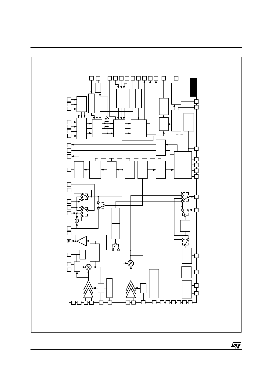
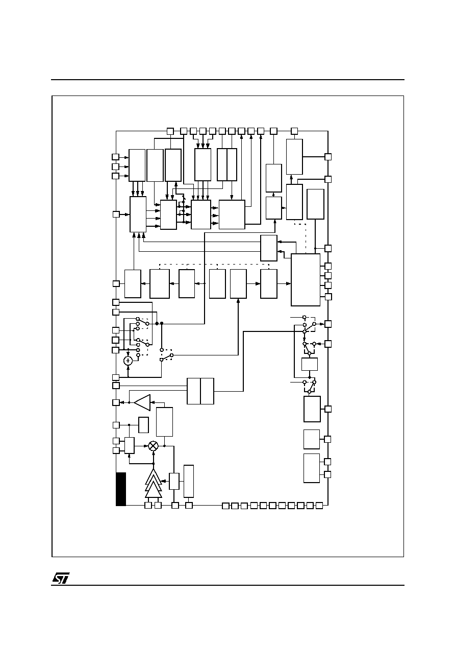
Figure 4. STV2237D (TQFP64) Block Diagram
S
T
V
223
7D
CVBSOUT2
CVBSOUT1
CVBSIN1
CVBSIN2
Y/CVBSIN3
INTCVBSOUT
FB
O
S
D
RO
S
D
GO
SD
BO
S
D
BC
L/
S
A
F
I
CAT
H
RO
UT
GO
U
T
BO
U
T
VE
R
T
HO
UT
RG
B
CO
NT
R
A
S
T
BC
L/
S
A
F
BR
IG
H
T
.
DRI
V
E
CUT-
O
FF
BL
A
N
KI
N
G
RG
B
SW
IT
C
H
LU
M
A
D
L
P
EAK
I
N
G
&
CO
RING
AC
C
& A
C
C
OV
ER
L
O
A
D
B
A
N
D
PAS
S
FI
L
T
E
R
LFB/SSC
I
≤C
B
U
S
DE
CO
DE
R
PLL
R
e
f
e
r
enc
e
Ca
rr
i
e
r
W/
B
S
P
O
T
IN
VE
R
T
E
R
V
REFIF
HC
AP
R
SLPF
X1/VAMP/CHROUT
CLPF
XTAL1
XTAL2
XTAL3
FMOUT/SC
EXTAUDIOIN
HO
RIZ
O
NT
A
L
2nd LO
O
P
HO
RIZ
O
NT
A
L
1
s
t
L
OOP
AU
T
O
I
D
EN
T
.
K
I
LLE
R
PA
L
/
N
T
S
C
DE
M
O
DUL
A
T
O
R
VER
T
I
C
A
L
S
C
A
NNING
S
Y
NC.
SE
P
CHR
O
M
A
DL
VA
M
P
D
C
CO
NT
RO
L
A
UDI
O
RE
F
BL
AC
K
ST
R
E
T
C
H
CHR
O
M
A
TR
A
P
FI
L
T
E
R
T
U
NI
NG
AG
C
T
UNE
R A
G
C
AG
C
S
O
UND B
P
FM D
E
M
O
D
D
E
EM
P.
FM
Mo
n
o
Mu
t
e
Mu
t
e
SA
T
.
/C
O
N
T
MA
TR
I
X
Sound Subcarriers
10
A
G
CS
I
F
CA
P
15
SAW
V
CCI
F
18
GN
D
IF
20
59
V
CC1
57
GN
D
1
V
CC2
27
G
ND2
25
9
SI
F
I
N
2
8
SI
F
I
N
1
PL
L
23
PIFLC1
24
PIFLC2
HA
L
F
C
T
R
YU
V
SW
IT
C
H
SAW
F
I
L
T
ER
S
W
I
T
CH CO
NTR
O
L
I
CAT
H
SEN
SE
AF
C
VO
L
U
M
E
AUDIOOUT
SCL
SDA
30
BEXT/Cb
31
GEXT/Y
32
REXT/Cr
33
FBEXT
38
VIN
37
UIN
39
YIN
41
VOUT
42
UOUT
40
YOUT
5
G
NDD
4
V
CCD
PI
F
I
N
1
14
PIF
I
N
2
13
16
TUNE
RA
G
C
O
U
T
12
AGC
P
I
F
C
A
P
17
IFPLL
7
FMCAP
35
CHR
29
BS
AVL
51
36
50
49
48
47
61
46
45
44
43
62
63
AP
R
RG
B
TO
Y
U
V
16
4
56
55
54
53
52
19
22
60
58
26
28
34
6
11
2
3
STV223XD/224XC - GENERAL DESCRIPTION
9/76
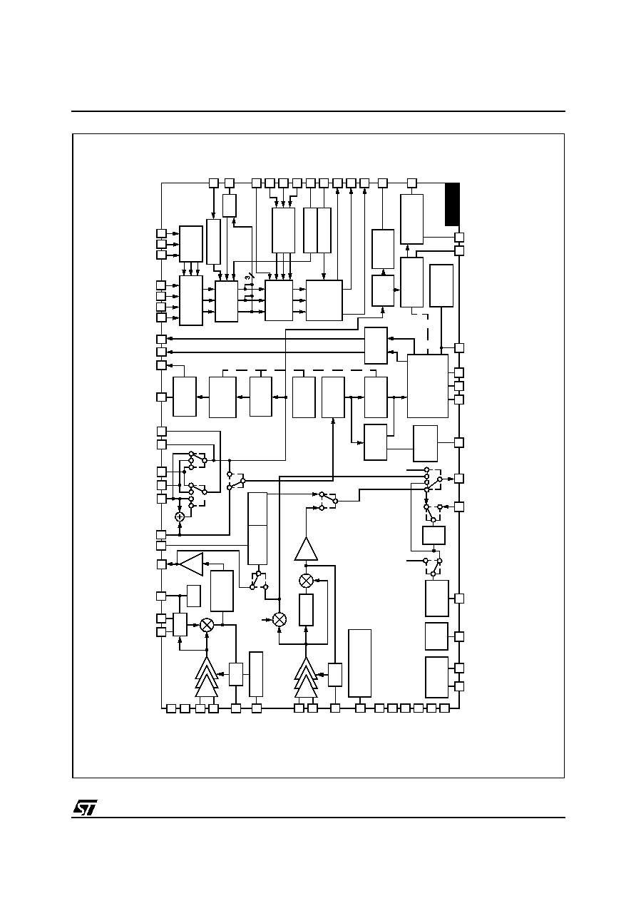
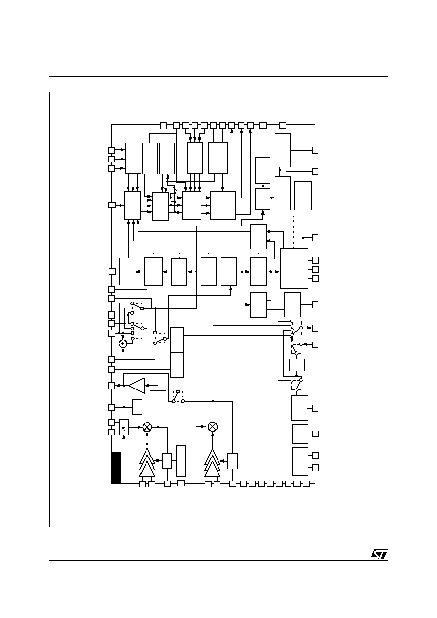
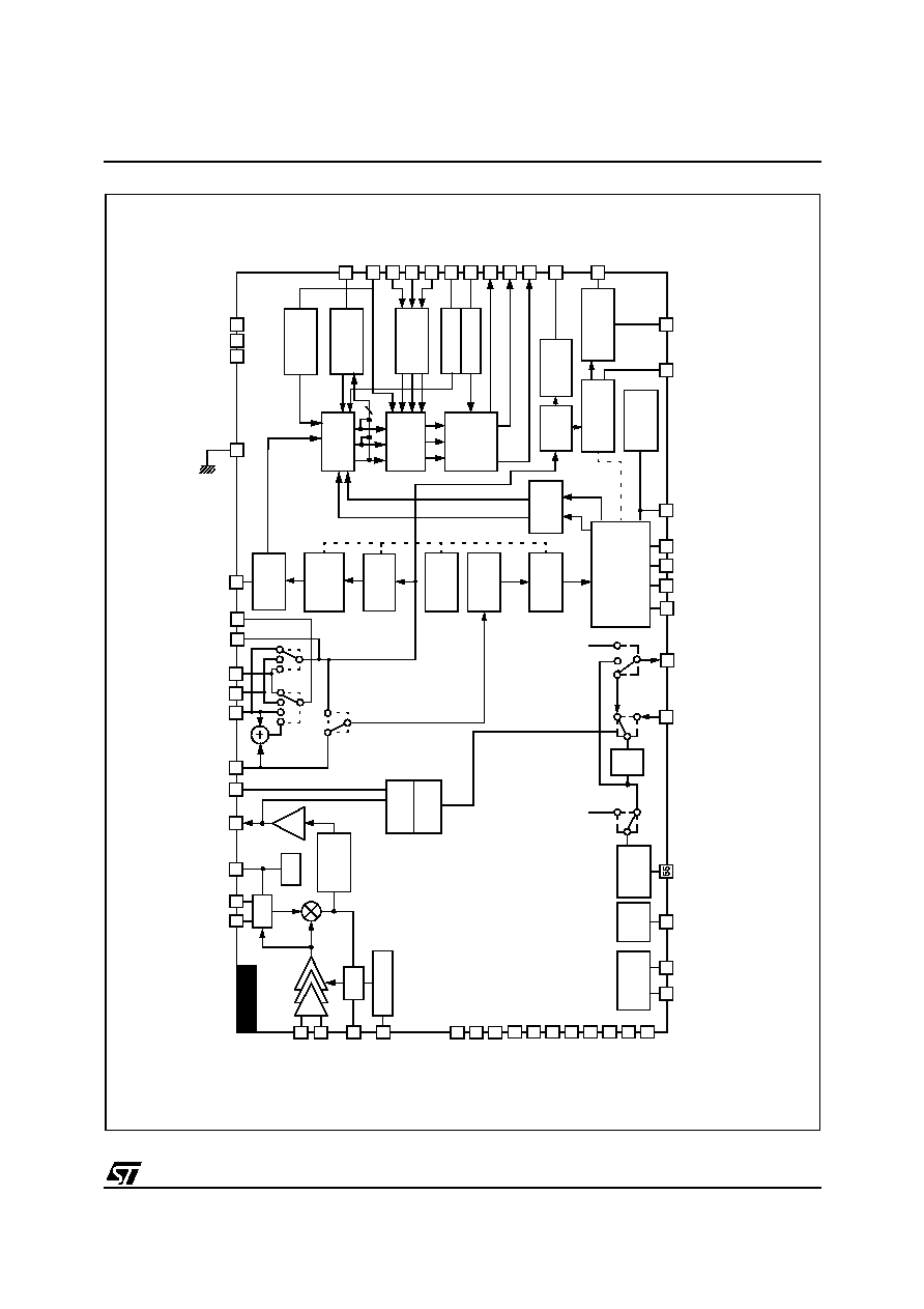
Figure 5. STV2238D (TQFP64) Block Diagram
ST
V2
2
3
8
D
CVBSOUT2
CVBSIN1
INTCVBSOUT
CVBSOUT1
CVBSIN2
Y/CVBSIN3
FB
O
S
D
RO
S
D
GOS
D
BOS
D
BC
L/
SAF
I
CAT
H
RO
UT
GOU
T
BOU
T
VE
R
T
HO
UT
BC
L/
SAF
RG
B
RG
B
TO
YU
V
RG
B
SW
IT
C
H
B
R
IGH
T
.
DRI
V
E
CUT-O
FF
BL
AN
KI
N
G
LFB/SSC
XTAL3/BTUN
B
A
NDP
A
S
S
FI
L
T
E
R
A
CC &
A
C
C
OV
ER
LO
AD
LU
M
A
D
L
PEA
KIN
G
&
CO
RI
NG
PL
L R
e
f
e
r
e
n
c
e
Ca
rr
i
e
r
I
≤C
B
U
S
DE
CO
DE
R
V
REFIF
HC
AP
R
HO
RIZ
O
NT
A
L
2nd L
O
O
P
HO
RIZ
O
NT
A
L
1s
t LO
O
P
A
U
TO
I
D
E
N
T.
KIL
L
E
R
P
A
L/
SEC
AM
/N
T
S
C
DE
MO
DUL
A
T
O
R
VER
T
I
C
A
L
S
C
A
NNING
S
Y
NC.
SE
P
CH
RO
MA
DL
VAM
P D
C
CO
NTR
O
L
AU
D
I
O
RE
F
BL
AC
K
ST
R
E
T
C
H
FI
L
T
E
R
TUNI
NG
CL
O
CHE
FI
L
T
E
R
CL
O
C
HE
TUNI
NG
AG
C
T
UNE
R A
G
C
AGC
FM
Mo
n
o
Mu
t
e
Mu
t
e
S
A
T
./C
ON
T
MA
T
R
I
X
Sound Subcarriers
10
AGC
S
I
F
C
A
P
15
SAW
V
CCI
F
18
GN
D
IF
20
59
V
CC1
57
G
ND1
V
CC2
27
G
ND2
25
9
SI
F
I
N
2
8
SI
F
I
N
1
23
PIFLC1
24
PIFLC2
PL
L
SA
W
F
I
L
T
ER
S
W
I
T
CH CO
N
T
RO
L
I
CAT
H
SEN
SE
YU
V
SW
I
T
C
H
AM
Mo
n
o
AF
C
AM/FMOUT/SC
EXTAUDIOIN
AUDIOOUT
VO
L
U
M
E
SCL
SDA
30
BEXT/Cb
31
GEXT/Y
32
REXT/Cr
33
FBEXT
38
VIN
37
UIN
39
YIN
41
VOUT
42
UOUT
40
YOUT
5
GN
D
D
4
V
CCD
PI
F
I
N
1
14
PI
F
I
N
2
13
16
TUNE
RA
G
C
O
U
T
12
AGC
P
I
F
C
A
P
17
IFPLL
7
FMCAP
35
CHR
29
BS
HA
L
F
C
T
R
AP
R
CO
NTR
A
S
T
SLPF
X1/VAMP/CHROUT
CLPF
XTAL1
XTAL2
LI
M
I
T
E
R
21
AV
L
51
36
50
49
48
47
61
46
45
44
62
43
63
64
1
56
55
54
53
52
19
22
6
11
W
/
B SPOT
IN
V
E
R
T
ER
60
58
26
28
34
2
3
CHR
O
M
A
TRA
P
D
EEM
P.
SO
U
N
D
BP
FM
DE
M
O
D
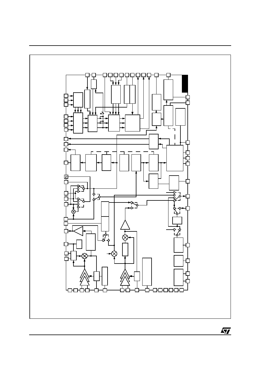
STV223XD/224XC - GENERAL DESCRIPTION
10/76
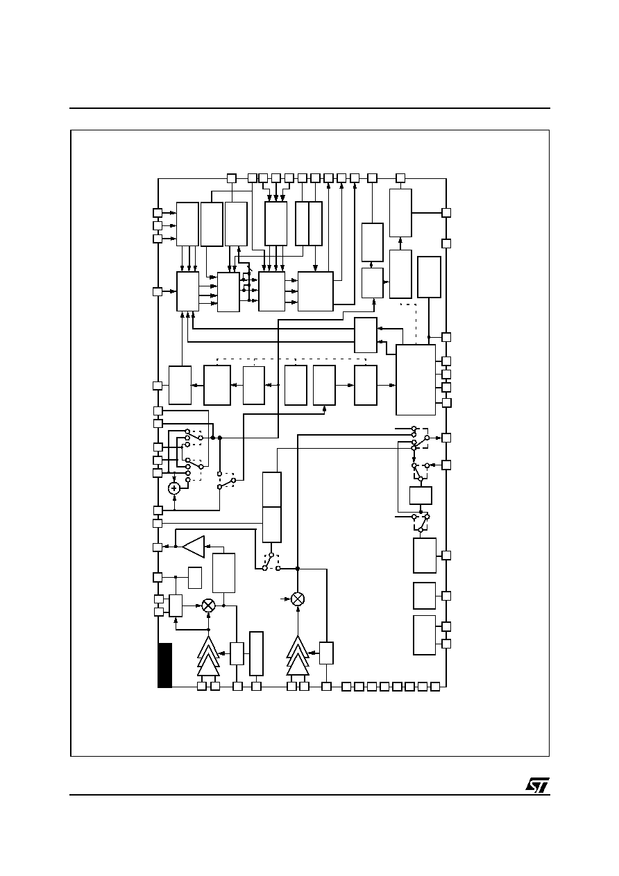
Figure 6. STV2239D (TQFP64) Block Diagram
ST
V2
2
3
9
D
INTCVBSOUT
HC
AP
R
FB
O
S
D
RO
S
D
GO
SD
BO
S
D
BC
L/
SAF
I
CAT
H
RO
UT
GOU
T
BO
U
T
VE
R
T
HO
UT
BC
L
/
SA
F
RG
B
CO
NT
R
A
S
T
RG
B
TO
Y
U
V
RG
B
SW
IT
C
H
BR
I
G
H
T
.
DRI
V
E
CUT
-O
F
F
BL
A
N
KI
N
G
LU
M
A
D
L
PE
AKI
N
G
&
CO
R
I
NG
AC
C
&
AC
C
OV
E
R
LOA
D
B
A
NDP
A
S
S
FI
L
T
E
R
XTAL3/BTUN
LFB/SSC
I
≤C B
U
S
D
E
CO
DE
R
W
/
B SP
O
T
IN
VER
T
E
R
P
LL R
e
f
e
r
enc
e
Ca
rri
e
r
CVBSOUT2
CVBSOUT1
CVBSIN1
CVBSIN2
Y/CVBSIN3
V
REFIF
HO
RIZ
O
NT
A
L
2nd LO
O
P
HO
RIZ
O
NT
A
L
1s
t LO
O
P
AU
T
O
I
D
EN
T
.
K
I
LLE
R
P
A
L
/
S
E
CA
M
/
NT
S
C
DE
M
O
D
U
L
A
T
O
R
VER
T
I
C
A
L
S
C
A
NNING
S
Y
NC.
SE
P
CHR
O
M
A
DL
VA
M
P
D
C
CO
NT
RO
L
A
UDI
O
RE
F
BL
AC
K
ST
R
E
T
C
H
CHRO
M
A
TR
A
P
FI
L
T
E
R
T
U
NI
NG
CL
O
CHE
FI
L
T
E
R
CL
O
CHE
T
UNI
NG
AG
C
T
UNE
R A
G
C
AG
C
S
O
UND B
P
FM D
E
M
O
D
D
E
EM
P.
FM
Mo
n
o
Mu
t
e
Mu
t
e
SA
T
.
/
C
O
N
T
MA
TR
I
X
Sound Subcarriers
10
A
G
CS
I
F
CA
P
15
SA
W
V
CCI
F
18
GN
D
IF
20
59
V
CC1
57
GN
D
1
V
CC2
27
G
ND2
25
9
SI
F
I
N
2
8
SI
F
I
N
1
23
PIFLC1
24
PIFLC2
PL
L
SA
W
F
I
L
T
ER
S
W
I
T
C
H
CO
NT
R
O
L
I
CA
T
H
SE
N
S
E
YU
V
SW
IT
C
H
AM
Mo
n
o
AF
C
SLPF
X1/VAMP/CHROUT
CLPF
XTAL1
XTAL2
FMOUT/SC
EXTAUDIOIN
AUDIOOUT
VO
L
U
M
E
SCL
SDA
HA
L
F
C
T
R
AP
R
41
VOUT
42
UOUT
40
YOUT
33
FBEXT
38
VIN
37
UIN
39
YIN
30
BEXT/Cb
31
GEXT/Y
32
REXT/Cr
5
GN
D
D
4
V
CCD
PI
F
I
N
1
14
PIF
I
N
2
13
16
T
U
N
E
R
A
GC
OU
T
12
A
G
CP
I
F
CA
P
17
IFPLL
7
FMCAP
35
CHR
21
29
BS
34
28
26
58
LI
M
I
T
E
R
AV
L
51
36
50
49
48
47
61
46
45
44
43
63
62
64
1
56
55
54
53
52
19
22
6
11
32
STV223XD/224XC - GENERAL DESCRIPTION
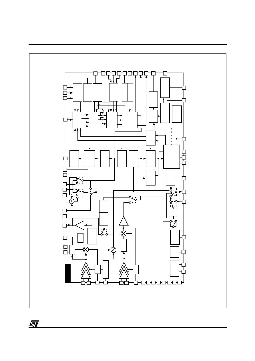
11/76
Figure 7. STV2246C (SDIP56) Block Diagram
S
T
V
2
24
6C
AP
R
BC
L
/
SA
F
RG
B
C
O
NT
RA
S
T
BR
I
G
H
T
.
DRI
V
E
CUT
-O
F
F
BL
AN
KI
N
G
RG
B
TO
Y
U
V
LU
M
A
D
L
P
EAK
IN
G
&
CO
RI
N
G
AC
C
&
AC
C
OV
E
R
LOA
D
B
A
NDP
A
S
S
FI
L
T
E
R
LFB/SSC
W/
B
S
P
O
T
IN
VE
R
T
E
R
F
M
M
ono
RG
B
AP
R
RO
S
D
GOS
D
BOS
D
BC
L/
SAF
I
CA
T
H
RO
U
T
GOU
T
BOU
T
VER
T
HO
U
T
FB
O
S
D
/
HC
3
HO
RIZ
O
NT
A
L
2nd LO
O
P
HO
RIZ
O
NT
A
L
1s
t LO
O
P
AU
T
O
I
D
EN
T
.
K
I
LLE
R
PA
L
/
N
T
SC
DE
M
O
DUL
A
T
O
R
VER
T
I
C
A
L
S
C
A
NNING
S
Y
NC.
SE
P
CHRO
M
A
DL
VA
M
P
D
C
CO
NT
R
O
L
I
≤C B
U
S
DE
CO
DE
R
A
UDI
O
RE
F
4 V
REF
SCL
SDA
52
51
BL
A
C
K
ST
R
E
T
C
H
CHRO
M
A
TR
A
P
FI
L
T
E
R
T
UNI
NG
AG
C
T
UNE
R A
G
C
SO
U
N
D
BP
FM
D
E
MO
D
DE
E
M
P
.
Mu
t
e
Mu
t
e
SA
T
.
/C
O
N
T
MA
TR
I
X
53
V
CCD
54
G
NDD
V
CCI
F
10
GN
D
IF
54
45
V
CC1
43
G
ND1
V
CC2
19
GN
D
2
17
1
NT
B
C
2
NT
B
C
3
NT
B
C
56
FMCAP
23
CHR
22
Y/CVBSIN3
20
CVBSIN2
18
CVBSIN1
44
CVBSOUT2
13
INTCVBSOUT
15
PIFLC1
16
PIFLC2
PL
L
I
CAT
H
SEN
S
E
7
PI
F
I
N
2
6
PI
F
I
N
1
8
T
UNE
RA
G
C
O
U
T
5
AG
C
P
IF
C
A
P
YU
V
SW
I
T
C
H
AF
C
HA
L
F
CO
N
T
RA
S
T
SLPF
X1/VAMP/CHROUT
FMOUT
EXTAUDIOIN
AUDIOOUT
CLPF
XTAL1
XTAL2
XTAL3
VO
L
U
M
E
F
M
M
ono
29
NTBC/CVBSOUT1
21
BS
28
FBEXT
27
REXT/Cr
26
GEXT/Y
25
BEXT/Cb
RG
B
SW
I
T
C
H
9
IFPLL
55
AV
L
24
37
36
35
34
46
33
32
31
30
47
48
49
50
42
41
40
39
38
11
14
STV223XD/224XC - GENERAL DESCRIPTION
12/76
Figure 8. STV2247C (SDIP56) Block Diagram
Sound
Subcarriers
ST
V2
2
4
7
C
AP
R
RG
B
CO
NT
RA
S
T
RG
B
SW
I
T
C
H
BR
I
G
H
T
.
DRI
V
E
CUT
-O
F
F
BL
A
N
KI
N
G
LU
M
M
A
D
L
PE
AK
I
N
G
&
CO
RI
NG
AC
C
& AC
C
OV
E
R
LOA
D
B
A
NDP
A
S
S
FI
L
T
E
R
W/
B
S
P
O
T
P
LL R
e
f
e
r
enc
e
Ca
rri
e
r
I
N
VER
T
E
R
LFB/SSC
APR
RO
S
D
F
B
O
S
D/
HC
GOSD
BOSD
BC
L/S
A
F
I
CA
T
H
RO
U
T
GOU
T
BOU
T
VER
T
HO
U
T
3
HO
R
I
Z
O
NT
A
L
2
nd LO
O
P
HO
RIZ
O
NT
A
L
1s
t LO
O
P
AU
T
O
I
D
EN
T
.
K
I
LLE
R
PA
L
/
N
T
S
C
DE
M
O
DUL
A
T
O
R
VE
R
T
I
C
A
L
S
C
A
NNING
S
Y
NC.
SE
P
CH
RO
M
A
DL
VA
M
P
D
C
CO
NT
RO
L
I
≤C B
U
S
DE
CO
DE
R
A
UDI
O
RE
F
4
V
REF
SCL
SDA
52
51
BL
A
C
K
ST
R
E
T
C
H
C
HRO
M
A
TR
A
P
FI
L
T
E
R
T
U
NI
NG
AG
C
T
UNE
R A
G
C
S
O
UND B
P
FM D
E
M
O
D
D
EEM
P.
FM
Mo
n
o
Mu
t
e
Mu
t
e
SA
T
.
/C
O
N
T
MA
TR
I
X
53
V
CCD
54
GN
D
D
V
CCI
F
10
GN
D
IF
54
45
V
CC1
43
G
ND1
V
CC2
19
GN
D
2
17
56
FMCAP
23
CHR
22
Y/CVBSIN3
20
CVBSIN2
18
CVBSIN1
44
CVBSOUT2
13
INTCVBSOUT
15
PIFLC1
16
PIFLC2
PL
L
AG
C
7
PI
F
I
N
2
6
PI
F
I
N
1
8
TU
NE
RA
G
C
O
U
T
5
A
G
CP
I
F
CA
P
YU
V
SW
IT
C
H
AF
C
SLPF
X1/VAMP/CHROUT
CLPF
XTAL1
XTAL2
XTAL3
FMOUT/SC
EXTAUDIOIN
VO
L
U
M
E
AUDIOOUT
29
NTBC/CVBSOUT1
21
BS
28
FBEXT
27
REXT/Cr
26
GEXT/Y
25
BEXT/Cb
IFPLL
9
1
SIF
I
N
1
2
SIF
I
N
2
3
AGC
S
IF
C
A
P
AVL
RG
B
TO
Y
U
V
HA
L
F
CO
NTRA
S
T
37
36
35
46
24
34
BC
L
/
SA
F
I
CA
TH
SE
N
S
E
32
31
30
47
48
33
50
49
42
41
40
39
38
11
14
55
STV223XD/224XC - GENERAL DESCRIPTION
13/76
Figure 9. STV2248C (SDIP56) Block Diagram
ST
V2
2
4
8
C
AP
R
BC
L
/
SAF
RG
B
CO
NT
RA
S
T
BR
I
G
H
T
.
DRI
V
E
C
U
T
OGG
BL
A
N
KI
N
G
LU
M
A
D
L
PEA
KIN
G
&
CO
RI
NG
AC
C
& A
C
C
OVE
R
L
O
AD
BA
N
D
PA
S
S
FI
L
T
E
R
Sound
Subcarrier
W/
B
S
P
O
T
I
N
VER
T
E
R
P
L
L R
e
f
e
r
e
nc
e
Ca
rr
ie
r
XTAL3/BTUN
RO
S
D
F
B
O
S
D/
HC
GOSD
BOSD
BC
L/S
A
F
I
CAT
H
RO
UT
GOU
T
BOU
T
VER
T
HO
UT
3
LFB/SSC
SLPF
X1/VAMP/CHROUT
CLPF
XTAL1
XTAL2
AM/FMOUT/SC
EXTAUDIOIN
AUDIOOUT
BL
AC
K
ST
R
E
T
C
H
CHRO
M
A
TR
A
P
FI
L
T
E
R
T
UNI
NG
CL
O
C
H
E
T
UNI
NG
SA
T
.
/C
O
N
T
MA
TR
I
X
YU
V
SW
I
T
C
H
D
E
EM
P.
FM
Mo
n
o
AM
Mo
n
o
49
Mu
t
e
SO
UND BP
FM
D
E
M
O
D
AG
C
AG
C
T
U
NE
R A
G
C
PL
L
AF
C
HO
RIZ
O
N
T
A
L
2nd LO
O
P
HO
RIZ
O
NT
A
L
1s
t LO
O
P
A
U
TO
I
D
E
N
T.
K
I
LLE
R
P
A
L
/
SEC
AM
/N
T
S
C
DE
M
O
DUL
A
T
O
R
VE
R
T
I
C
A
L
S
C
A
NNING
S
Y
NC.
SEP
CHRO
M
A
DL
VA
M
P
D
C
CO
NT
RO
L
I
≤C
B
U
S
DE
CO
DE
R
A
UDI
O
RE
F
4
V
REF
SCL
SDA
52
51
53
V
CCD
54
G
NDD
V
CCI
F
10
GN
D
IF
54
45
V
CC1
43
GN
D
1
V
CC2
19
GN
D
2
17
56
FMCAP
23
CHR
22
Y/CVBSIN3
20
CVBSIN2
18
CVBSIN1
44
CVBSOUT2
13
INTCVBSOUT
29
NTBC/CVBSOUT1
15
PIFLC1
16
PIFLC2
7
PI
F
I
N
2
6
PI
F
I
N
1
HA
L
F
CO
NTRA
S
T
VO
LU
M
E
21
BS
28
FBEXT
27
REXT/Cr
26
GEXT/Y
25
BEXT/Cb
IFPLL
9
1
SI
F
I
N
1
2
SI
F
I
N
2
5
A
G
CP
I
F
CA
P
8
T
UNE
RA
G
C
O
U
T
3
A
G
CS
I
F
CA
P
RG
B
TO
Y
U
V
LI
M
I
T
E
R
I
C
ATH
SEN
SE
AV
L
37
36
35
34
24
AP
R
46
33
32
31
30
47
48
50
Mu
t
e
42
41
40
39
38
11
14
55
CL
O
CHE
FI
L
T
E
R
RG
B
SW
I
T
C
H
STV223XD/224XC - GENERAL DESCRIPTION
14/76
Figure 10. STV2249C (SDIP56) Block Diagram
ST
V2
2
4
9
C
INTCVBSOUT
AP
R
RG
B
CO
NT
R
A
S
T
RG
B
TO
Y
U
V
RG
B
SW
IT
C
H
LU
M
A
D
L
P
EAK
IN
G
&
CO
RI
NG
AC
C
& AC
C
OV
E
R
LOA
D
B
A
NDP
A
S
S
FI
L
T
E
R
Sound Subcarrier
XTAL3/BTUN
W
/
B SP
O
T
P
LL R
e
f
e
r
enc
e
IN
VER
T
E
R
Ca
rri
e
r
CVBSOUT2
CVBSIN1
CVBSIN2
Y/CVBSIN3
BR
I
G
H
T
.
DRI
V
E
CUT
-O
F
F
BL
A
N
KI
N
G
LFB/SSC
APR
RO
S
D
FB
O
S
D/
HC
GO
S
D
BO
S
D
BC
L/
S
A
F
I
CA
T
H
RO
UT
GO
U
T
BO
U
T
VE
R
T
HO
UT
3
HO
RIZ
O
NT
A
L
2nd
LO
O
P
HO
RIZ
O
NT
A
L
1
s
t
L
OOP
AU
T
O
I
D
EN
T
.
K
I
LLE
R
P
A
L
/
S
E
CA
M
/
NT
S
C
DE
M
O
DUL
A
T
O
R
VE
R
T
I
C
A
L
S
C
A
NNING
S
Y
NC.
SEP
CHRO
M
A
DL
VA
M
P
D
C
CO
NT
RO
L
I
≤C B
U
S
DE
CO
DE
R
A
UDI
O
RE
F
4
V
REF
SCL
SDA
52
51
BL
A
C
K
ST
R
E
T
C
H
CHRO
M
A
TR
A
P
FI
L
T
E
R
T
UNI
NG
CL
O
CHE
FI
L
T
E
R
CL
O
CHE
T
UNI
NG
AG
C
T
UNE
R A
G
C
S
O
UND B
P
FM
D
E
MO
D
D
E
EM
P.
FM
Mono
Mu
t
e
Mu
t
e
SA
T
.
/
C
O
N
T
MA
TR
I
X
53
V
CCD
54
G
NDD
V
CCI
F
10
GN
D
IF
54
45
V
CC1
43
GN
D
1
V
CC2
19
G
ND2
17
15
PIFLC1
16
PIFLC2
YU
V
SW
IT
C
H
AF
C
7
PI
F
I
N
2
6
PI
F
I
N
1
VO
L
U
M
E
FMOUT/SC
EXTAUDIOIN
AUDIOOUT
22
18
20
44
NTBC/CVBSOUT1
29
21
BS
28
FBEXT
27
REXT/Cr
26
GEXT/Y
25
BEXT/Cb
SLPF
X1/VAMP/CHROUT
CLPF
XTAL1
XTAL2
IFPLL
9
56
FMCAP
23
CHR
13
1
SI
F
I
N
1
2
SI
F
I
N
2
3
AG
C
S
IF
C
A
P
5
A
G
CP
I
F
CA
P
8
TUNE
RA
G
C
O
U
T
BC
L
/
SA
F
I
CA
TH
SE
N
S
E
HA
L
F
CO
NT
R
A
S
T
AVL
24
37
36
35
34
46
33
32
30
47
48
31
49
50
42
41
40
39
38
11
14
55
AG
C
STV223XD/224XC - GENERAL DESCRIPTION
15/76
Figure 11. STV2286C (SDIP56) Block Diagram
ST
V2
2
8
6
C
APR
RG
B
C
O
NT
RA
S
T
BC
L
/
SA
F
RG
B
SW
I
T
C
H
BR
IG
H
T
.
DR
I
V
E
CUT
-O
F
F
BL
A
N
KI
N
G
BAN
D
P
A
S
S
FI
L
T
E
R
AC
C
& AC
C
OV
E
R
L
O
A
D
LU
M
A
D
L
PEA
KI
N
G
&
CO
RI
NG
LFB/SSC
I
≤C B
U
S
DE
CO
DE
R
W
/
B SP
O
T
IN
V
E
R
T
ER
F
M
M
ono
RO
S
D
FB
O
S
D/
HC
GO
S
D
BO
S
D
BC
L/
S
A
F
I
CA
T
H
RO
UT
GO
U
T
BO
U
T
VE
R
T
HO
UT
3
HO
RIZ
O
NT
A
L
2nd LO
O
P
HO
RIZ
O
NT
A
L
1s
t LO
O
P
A
U
TO
I
D
E
N
T.
K
I
LLE
R
PAL
/
N
T
S
C
DE
M
O
DUL
A
T
O
R
VE
R
T
I
C
A
L
S
C
A
NNING
S
Y
NC.
SE
P
C
HRO
M
A
DL
VA
M
P
D
C
CO
NT
RO
L
A
UDI
O
RE
F
4
V
REF
SCL
SDA
52
51
BL
A
C
K
ST
R
E
T
C
H
FI
L
T
E
R
T
UNI
N
G
AG
C
T
UNE
R A
G
C
SO
U
N
D
BP
FM
D
E
M
O
D
D
E
EM
P.
Mu
t
e
Mu
t
e
SA
T
.
/C
O
N
T
MA
TR
I
X
53
V
CCD
54
GN
D
D
V
CCI
F
10
GN
D
IF
54
45
V
CC1
43
G
ND1
V
CC2
19
G
ND2
17
1
NTB
C
2
NTB
C
3
NTB
C
15
PIFLC1
16
PIFLC2
AP
R
8
T
U
NE
RA
G
C
O
U
T
5
A
G
CP
I
F
CA
P
AF
C
7
PI
F
I
N
2
6
PI
F
I
N
1
HA
L
F
CO
NT
R
A
S
T
SLPF
X1/VAMP/CHROUT
CLPF
XTAL1
XTAL2
XTAL3
FMOUT
EXTAUDIOIN
AUDIOOUT
VO
L
U
M
E
NTBC
27
NTBC
26
NTBC
25
28
BS
21
CVBSOUT2
44
NTBC/CVBSOUT1
29
CVBSIN1
CVBSIN2
Y/CVBSIN3
18
20
22
CHR
FMCAP
INTCVBSOUT
23
56
13
IFPLL
9
PL
L
42
41
40
39
38
11
14
CH
RO
M
A
TR
A
P
AVL
I
CA
TH
SE
N
S
E
37
36
35
34
46
24
33
32
31
30
47
48
49
50

STV223XD/224XC - STV2238D MAIN FEATURES
16/76
2 STV2238D MAIN FEATURES
s
I≤C Bus control (Read and Write modes).
s
PLL PIF demodulator, bus-controlled VCO
alignment.
s
Positive and negative IF modulation.
s
Digital AFC.
s
Tuner-delayed AGC output.
s
White and Black Spot cancellation.
s
SIF with QSS structure.
s
Intercarrier capability.
s
Built-in sound bandpass.
s
Multistandard PLL FM Demodulator (4.5, 5.5,
6.0, 6.5 MHz).
s
AM demodulator for France.
s
Sound subcarrier output for Stereo chassis: FM
and NICAM carriers.
s
Audio switch for external audio input, Mono
chassis.
s
Digital volume control.
s
Audio Mute.
s
Automatic Volume Levelling (AVL) on audio
signal (internal or external audio).
s
Digital buffer for SAW filter switching.
s
Video switch, three Composite Video
Broadcasting Signal (CVBS) inputs and two
CVBS outputs (which can be used to drive a
teletext decoder).
s
SVHS switch, Y input is combined with CVBS3
input.
s
Capability to output Y+C signal on second
CVBS output.
s
OSD RGB analog inputs, fast blanking
detection on fast blanking OSD pin, contrast
control capability.
s
Half-contrast control pin.
s
External analog RGB inputs with contrast and
saturation control (external RGB matrixed in
YUV). External analog YCrCb inputs can be
connected to the same inputs. In this case, the
sync signal must be sent to the CVBS input, and
External YCrCb mode must be selected through
the I≤C bus.
s
Y,U,V inputs outputs: Y,U,V inputs/outputs for
the use of enhanced picture ICs.
s
Integrated chroma filters (trap, bandpass,
cloche) with automatic alignment.
s
Integrated luminance delay line.
s
Adjustable peaking on the luminance signal with
coring function.
s
Black Stretch circuit.
s
Automatic RGB peak regulation (APR).
s
PAL/SECAM/NTSC color decoder with
automatic identification of standards.
s
Integrated chroma delay line.
s
Full integrated SECAM decoder.
s
Hue control, two selectable matrices in NTSC
mode.
s
Automatic Flesh Control circuit with two
selectable characteristics (normal and wide).
s
ACC overload circuit.
s
Chroma subcarrier output which could be used
to drive a comb filter circuit.
s
Automatic digital cut-off current loop with warm-
up detection circuit.
s
White point (drive) and cut-off point
adjustments.
s
Manual cut-off capability.
s
Beam current limiter control stage.
s
High performance synchronization pulses
separator.
s
Horizontal synchronization with two phase-
locked loops.
s
Integrated VCO, auto-calibration using the
chroma crystal reference frequency.
s
Automatic time constant selection for the first
PLL, three selectable time constants.
s
Video identification circuit (independent from
PLL1).
s
Noise detector circuit.
s
Vertical countdown circuit.
s
Automatic 50/60 Hz selection circuit.
s
Blanking and inserted cut-off pulses position
adapted to standard (50 or 60 Hz).
s
Long blanking mode capability in 60 Hz (same
blanking as with 50 Hz standard).
s
Possibility of inserting cut-off pulses after a
vertical oversize blanking signal.
s
De-interlace capability.
s
Horizontal starting circuit with soft-start
capability.
s
Horizontal and vertical position adjustments,
vertical amplitude control voltage (combined
with chroma subcarrier output).
s
4/3, 16/9 selection voltage.
s
Oversize Blanking capability on OSD Fast
Blanking input.

STV223XD/224XC - FUNCTIONAL DESCRIPTION
17/76
3 FUNCTIONAL DESCRIPTION
The STV2238D is an integrated device that proc-
esses PIF, SIF, Video and Chroma signals while
scanning for PAL, SECAM and NTSC standards. It
includes a base band chroma delay line, Video,
SVHS and audio switches.
3.1 DETAILED FEATURES
3.1.1 Power Supplies
V
CCIF
: 5 V power supply dedicated to IF proces-
sors.
V
CCD
: 5 V power supply dedicated to I≤C bus and
digital parts. GNDD is the ground reference of
these parts.
V
CC1
: 8 V power supply for video switches, scan-
ning part and the chroma decoder. GND 1 is the
ground reference of all these functions.
V
CC2
: 8 V power supply for the luminance, RGB
processing parts audio switch and internal CVBS
output. GND2 is the ground reference of these
parts.
3.1.2 Picture Intermediate Frequency (PIF)
≠ AGC amplifier.
≠ PLL synchronous demodulator. Bus-controlled
VCO for integrated tuning of the external LC res-
onator. For a 38.9 MHz VCO, the LC coil specifi-
cation has to be:
C = 39pF, f = 44 MHz ±2% (LC not connected).
For a 33.9 MHz VCO (L'), the VCO can be
switched via the bus control.
≠ Digital AFC via bus.
≠ IF Automatic Gain Control (AGC)
Negative modulation: top sync regulation, regu-
lation of overmodulated signals (overmodulation
regulation circuit enabled through bus control).
Positive modulation: main regulation on white
level with black level limitation.
≠ Tuner-delayed AGC with bus control for AGC
gain and threshold. When tuner AGC output is
active, read register 03hex, data D7 is set to "1".
≠ CVBS output with 2 bus-controlled amplitudes.
CVBS output at 2 V
PP
if external sound trap is
not connected (QSS mode). CVBS output at 2.3
V
PP
if external sound trap is connected (Intercar-
rier mode).
3.1.3 Sound Intermediate Frequency (SIF) and
Sound Demodulators
≠ QSS structure.
≠ SIF Automatic Gain Control (QSS mode).
≠ Built-in sound bandpass.
≠ PLL FM Demodulator for 4.5, 5.5, 6.0 or 6.5 MHz
carriers. The Sound Standard is selected by the
MCU. The FM demodulator VCO is automatically
calibrated using the chroma crystal VCO refer-
ence frequency. The FM Demodulator VCO is
automatically calibrated for all sound standards
independently of the chroma crystal VCO fre-
quency, which is either 4.4 MHz or 3.5 MHz. For
each sound carrier frequency, the IC sends an
indication of the sound subcarrier level to the
MCU so that it can select the proper standard.
≠ The sound subcarrier level is valid when the FM
Demodulation VCO is calibrated. This informa-
tion can be read via the I≤C Bus.
≠ Bus controls for FM de-emphasis (50 or 75 µs)
and FM deviation ±25 or ±50 kHz).
≠ AM demodulator.
≠ Sound demodulator output: either an AM or FM
signal can be the output for the Mono chassis
≠ Sound subcarriers for the Stereo chassis.
3.1.4 Audio Switch
≠ One SCART switch.
≠ Bus-controlled volume and mute. Zero-crossing
function on volume control.
≠ Automatic Volume Levelling (AVL) function can
be enabled via the I≤C bus. Two time constants
(gain increase) can be selected via the I≤C bus.
≠ The AM sound can be selected on the main au-
dio output for the Stereo chassis.
3.1.5 Surface Acoustic Wave (SAW) Filter
Switch Control
≠ SAW filter switch control pin is available in the
TQFP64 package. The SAW filter switch control
pin is used to select the correct SAW filter char-
acteristics (e.g.: M/N or BGDK characteristics).
In a multi-standard chassis, two output voltages
are selected via the I≤C bus (low level voltage at
0.4 V Max., and high level voltage at 4 V Min.).
3.1.6 Video Switches
≠ Video switch with three CVBS inputs and one
CVBS output (CVBSOUT1) which may be used
to drive a teletext decoder.
≠ A second CVBS output (CVBSOUT2) is able to
output recombined Y+C signals.
All switches are independently controlled.
≠ SVHS switch, Y input is combined with CVBS 3
input. CVBS/SVHS modes can be selected ei-
ther by bus control (software selection), or by
sensing the DC voltage on the Chroma Input pin
(hardware selection). If the Chroma Input is

STV223XD/224XC - FUNCTIONAL DESCRIPTION
18/76
grounded, the CVBS mode is selected and the
bus control is not active. If the DC level of the
Chroma Input is higher than the SVHS threshold,
then the bus control for the SVHS switch is ac-
tive. Therefore, the SVHS mode can be selected
by hardware using a special SVHS connector
that includes a mechanical switch. In this type of
application, the bus control is set to SVHS mode,
and the CVBS mode is selected by grounding the
Chroma Input pin.
3.2 DEFLECTION PART
≠ Fully-integrated synchronization separator with a
low pass filter, black level alignment of the CVBS
input, and a 50% slicing level for the synchro-
nized pulse amplitude.
≠ Vertical output pulse is locked on a pulse that is
twice the horizontal frequency to ensure perfect
interlacing.
≠ Auto-calibrated VCO using the chroma crystal
reference. Crystal control pin X1/VAMP/
CHROUT indicates the crystal reference value
on Pin XTAL1.
When a 4.43 MHz crystal is connected to
Pin XTAL1, the output load on Pin X1/VAMP/
CHROUT must be greater than 80 k
. When a
3.58 MHz crystal is connected to Pin XTAL1, the
output load must be less than 10 k
.
Two Phase-locked Loops (PLL):
≠ The first PLL locks the VCO to the video line fre-
quency,
≠ The second PLL compensates the line transistor
storage time.
Three time constants for the first PLL.
≠ [X,Y]: Line number referring to the internal line
counter numbering system.
The long time constant is used for normal opera-
tion.
The short time constant is automatically used dur-
ing the VCR search mode and frame retrace when
the frame pulse is outside [258,264] and
[309,314].
The very long time constant is used when there is
no video recognition (very good OSD stability).
Time constants in normal operation (automatic se-
lection of time constants):
≠ 50 Hz input signal:
short time constant: [306,21],
long time constant: the rest of the field.
≠ 60 Hz input signal:
short time constant: [0,16],
long time constant: the rest of the field.
Inhibition of the first PLL:
The first PLL is inhibited from line 309 to line 4.5
(or 314) in 50 Hz mode and from line 258 to line
5.5 (or 264) in 60 Hz mode. The time constant val-
ues are chosen by means of external components.
≠ Possibility of forcing the short time constant dur-
ing the allframe via the bus.
≠ Possibility of forcing the long time constant dur-
ing the allframe via the bus.
≠ Possibility of forcing a very long time constant
during the allframe via the bus.
Video identification: independent from PLL1.
The video identification status is available in the
output register of the I≤C bus decoder.
Generation of burst gate pulses and line frequency
signals from the first PLL to drive the Chroma and
Video circuits.The burst gate pulse is also sent to
the super-sandcastle generator.
Frame synchronized window:
≠ large window: [248,352] in AUTO mode,
[248,284] in forced 60 Hz mode, [288,352] in
forced 50 Hz mode.
≠ narrow window: [309,314] in 50 Hz mode,
[258,264] in 60 Hz mode.
Field frequency selection windows:
≠ [248,286] 60 Hz mode selection window.
≠ [288,352] 50 Hz mode selection window.
Frame blanking pulse adapted to standard:
≠ from line 309 to line 21 in 50 Hz mode,
≠ from line 258 to line 16 in 60 Hz mode.
Long blanking mode: the end of frame blanking is
line 21 both in 50 and 60 Hz modes. This mode is
useful when the flyback time of the vertical output
stage is longer than the 60 Hz blanking time. It is
used to optimize the 50/60 Hz vertical amplifier ap-
plication due to long frame blanking.
Vertical output pulse duration is 10.5 lines.
Horizontal output pulse: 28 µs line pulse on an
open collector output.
Start-up circuit: the horizontal output is at high lev-
el (disabled) when V
CC1
increases from 0 to 6.0 V
and when V
CCD
has not reached 4 V.
Soft mode circuit: it provides a softer operating
horizontal output with a 75% duty cycle [t
HIGH
/
(t
HIGH
+t
LOW
)]. This results in a smaller conducting
time (16 µs instead of 28 µs).
This mode is active at start-up until two frames af-
ter the V
CC2
reaches 75% of the V
CC1
. It is also
active at shutdown when the V
CC1
floats between
6 V and 5.4 V. And finally, this mode is used if the
V
CC2
drops below 75% of the V
CC1
.

STV223XD/224XC - FUNCTIONAL DESCRIPTION
19/76
At shutdown, horizontal pulses are disabled when
V
CC1
is less than 5.4 V or when V
CCD
is less than
3.5 V.
The horizontal output pulse may be disabled via
the bus (force a high level on HOUT).
Safety input on BCL Pin. When the BCL Pin is
switched to ground, the horizontal output pulse is
disabled and the inhibition of horizontal output
pulse is maintained until V
CC1
is less than 3 V
(V
CC1
power supply is switched off). The Safety
function can be disabled via the I≤C bus. When
register 15hex data D7 is set to "1", the Safety
function is reset and no longer active.
The horizontal position adjustment is controlled via
the bus.
Bus-controlled DC output voltage for adjusting the
vertical amplitude. This voltage supply is used to
adjust the slope of the vertical sawtooth generated
by the external vertical booster.
Bus-controlled vertical position. The high level of
the vertical pulse is used to adjust the vertical po-
sition.
Bus-controlled 4/3-16/9 selection. 0.2 V is the low
level of the vertical pulse when 16/9 is selected
and 2 V when 4/3 is selected.
The Oversized Blanking function is controlled by
the voltage on the FBOSD pin. When the FBOSD
voltage is between the first and the second thresh-
olds, the OSD RGB signals are selected. When
the FBOSD voltage is greater than the second
threshold (4 V blanking threshold), the RGB out-
puts are blanked during the whole field, but not
during inserted cut-off lines (the cut-off loop is al-
ways active). The blanking feature, via the FBOSD
input pin, enables Vertical Oversize Blanking
when a 4/3 picture is displayed on a 16/9 screen in
Zoom mode. The picture outside the screen is
blanked by the Oversize Blanking pulse supplied
by the external vertical IC (STV9306).
Combined Flyback input and Super-Sandcastle
output: The line blanking level is clamped at 3 V,
the burst key pulse voltage is 5 V and vertical
pulse voltage is 2 V. The line pulse is extracted
with a 2.5 V slicing level used for RGB line blank-
ing and PLL2 control.
3.3 FILTERS
Integrated Trap Filter
Q = 1.5 (f-3dB = f0 (1-1/2Q)),
Center frequency:
≠ 4.43 MHz, 3.58 MHz for PAL and NTSC.
≠ 4.25 MHz, for SECAM
(-20 dB rejection between 4.1 MHz and
4.4 MHz).
The chroma trap filter is switched off in SVHS
mode, or in color standard search mode (standard
not identified). The trap filter can be switched off
via the bus.
Integrated Chroma Bandpass
Q = 3.5, Center frequency: 4.43 MHz, 3.58 MHz.
The Bus Control Frequency Shift is used to opti-
mize the chroma response for the video signal
from the IF stage.
Integrated Bell Filter for SECAM
Q = 16, Center frequency: 4.286 MHz.
The Bus Control Frequency Shift is used to opti-
mize the chroma response for the video signal
from the IF stage.
Integrated Luma Delay Line
Bandwidth: 8 MHz.
The Luma Delay Line is automatically adapted to
the chroma standard. For PAL BG and applica-
tions without group delay compensation, a Luma
Delay Shift of -140 ns can be selected via the I≤C
bus.
Filter Tuning
All filters are tuned via a reference phase-locked
loop. The PLL is based on a trap filter, a phase
comparator and an internal loop filter (capacitor).
The reference signal is the continuous carrier
wave from the Chroma VCO (4.43 MHz or
3.58 MHz). The PLL adjusts the center frequency
of the trap until it equals the reference signal.The
PLL tuning voltage is used to adjust all other inte-
grated filters. The Bell filter is fine-tuned with a
second PLL during the frame retrace. The Bell fil-
ter tuning voltage is memorized on an external ca-
pacitor (BTUN Pin).

STV223XD/224XC - FUNCTIONAL DESCRIPTION
20/76
3.4 VIDEO CIRCUIT
RGB Inputs
The RGB (OSD) input has priority over the exter-
nal RGB input. The RGB (EXT) source is matrixed
into YUV signals for color and contrast adjust-
ments. The brightness is adjusted according to the
internal and external RGB and OSD RGB signals.
The Contrast Control regulates both external and
internal RGB signals and has a maximum attenua-
tion of -24 dB. It also regulates the OSD RGB sig-
nal and its maximum attenuation is limited to
-12 dB. The Contrast Control for RGB (OSD) input
can be disabled via the bus. The brightness of the
RGB (OSD) input varies according to the main
brightness level.
The RGB (EXT) insertion signal can be disabled or
forced via the bus. A fast blanking detector on an
external fast blanking input and OSD fast blanking
input operate during frame retrace. The Fast
Blanking detection status is sent to the I≤C bus
read register.
The OSD fast blanking input has several functions:
OSD Insertion Control, RGB Output Blanking or
Half Contrast Control.
Half-contrast Control Pin (TQFP64)
The 6 dB gain reduction will be applied to the inter-
nal YUV signals when the half-contrast function is
turned ON, and the voltage of the half-contrast in-
put exceeds the threshold (0.7 V Typ.).
The Half Contrast function is also available in the
SDIP56 package. The Half Contrast input is com-
bined with the FBOSD input.
Automatic Cut-off Current Loop
The Cut-off Loop range is 2 V (the cut-off level of
the RGB outputs is between 1.5 V and 3.5 V,
2.5 V Typ.). The cut-off current is measured se-
quentially during the three lines after the internal
frame blanking signal (the blue cathode current is
measured first, then the green and red). The Leak-
age cathode current is measured during frame
blanking and is memorized on an internal capaci-
tor. Cut-off pulses can be inserted after the exter-
nal vertical oversize blanking signal. The Cut-off
loop can be frozen via the bus. To prevent cut-off
lines from being visible in 16/9 mode, cut-off puls-
es are not inserted when the cut-off loop is frozen.
Warm-up Detector
At power on, the cut-off loop is not active and high
DC levels are inserted during "cut-off" lines. The
Cut-off loop will be active when the cathode cur-
rent reaches the warm-up detection threshold.
This causes the picture to be displayed from a
dark screen. The RGB outputs are blanked until
cut-off current is close to the reference voltage.
The manual cut-off mode can be selected via the
I≤C bus. In this mode, the I
CATH
input pin is inac-
tive and cut-off pulses are not inserted. The RGB
black levels are independently controlled by three
I≤C bus registers (8-bit resolution). The black level
of each RGB output can be adjusted within a
range of 2.5V typ.
Beam Current Limiter DC Voltage Input (BCL)
The BCL will first decrease the contrast and then
the brightness when the contrast attenuation
reaches -5 dB. The red, green, blue channel gain
for white point adjustment takes place via the bus.
The red and green DC levels for black point adjust-
ment takes place via the bus.
The PAL/SECAM matrix is provided and a specific
NTSC matrix is used when demodulation angles
are (0∞,104∞).
Bus-controlled Contrast and Saturation
The Contrast Control regulates internal RGB, ex-
ternal RGB and OSD RGB inputs. The maximum
attenuation on internal and external RGB inputs is
-24 dB and is limited to -12 dB for OSD RGB in-
puts. The bus-controlled saturation range is 50 dB.
Bus-controlled Brightness and Sharpness
The total brightness range is 60% of the black-to-
white amplitude at maximum contrast. The bright-
ness control regulates all RGB sources (internal,
external and OSD). Bus-controlled Sharpness
(peaking) is provided in PAL/SECAM/NTSC
standards.
Bus-controlled Coring function on Sharpness
When the Coring-on-sharpness function is
switched ON, the peaking function is not active on
low amplitude signals (below 10 IRE).
The Black Stretch circuit can be disabled via the
bus. Two modes are provided, one to be used
when the video signal is transmitted with a set-up
(7.5IRE set-up in NTSC), the other to be used
when the video signal is transmitted without a set-
up (PAL/SECAM).
The bus-controlled Blue Screen feature is used to
insert a blue background on the screen when no
video is available. The RGB OSD can be dis-
played when the blue screen is active.
The APR (Automatic RGB Peak Regulation) func-
tion is used to take advantage of the total RGB
output range. APR circuits detect the peak level of
the RGB outputs (before OSD insertion) and regu-
late the RGB gain (contrast) so that signals above
the APR threshold are limited. For example, at
maximum drive and contrast levels with the APR
function switched OFF, the 100 IRE input signal
gives 3 V(B/W) to the RGB outputs. With APR ON
and the APR threshold at 70 IRE, the 70 IRE input
signal gives 3 V (B/W) at RGB outputs. For input

STV223XD/224XC - FUNCTIONAL DESCRIPTION
21/76
signals above 70 IRE, the APR will decrease the
RGB gain so that amplitude at the RGB output is
always 3 V (B/W). The APR gain control voltage is
memorized on an external capacitor where the
gain decrease is very fast and the gain increase is
very slow (several frames). The APR function can
be enabled or disabled via the I≤C bus.
3.5 CHROMA CIRCUIT
PAL/SECAM/NTSC Decoders
SVHS Chroma input; bus-controlled SVHS mode.
≠ 30 dB ACC range.
≠ Integrated chroma base band delay line and ON/
OFF bus control.
≠ Automatic standard identification, with possibility
of forcing the standard via the bus.
≠ 3-crystal application capability for the South
American market:
The first crystal on Pin XTAL1 (3.5X MHz only),
he second crystal on Pin XTAL2 (3.5X MHz on-
ly), and the third crystal on Pin XTAL3/BTUN
(3.5X MHz only, used for PAL/NTSC application
only).
PAL/NTSC Decoder
ACC carried out by peak detector on synchronous
demodulation of the burst.
Fully-integrated killer function.
VCO using two standard crystals: 4.43 MHz and
3.58 MHz. One crystal is internally selected de-
pending on the standard selection. A third crystal
can be used in PAL/NTSC applications only.
VCO reference signal is available on Pin X1.
≠ 4.433619 MHz XTAL specification.
Mode of operation: serial resistance (without
load capacity),
Motional capacitance: C
M
= 13fF ±3fF,
Shunt capacitance: C
P
< 7pF,
Serial resistance: R
S
< 70
.
≠ 3.579545 MHz XTAL specification (NTSC M).
Mode of operation: serial resistance (without
load capacity),
Motional capacitance: C
M
= 11fF ±3fF,
Shunt capacitance: C
P
< 7 pF,
Serial resistance: R
S
< 70
.
≠ 3.575611 MHz XTAL specification (PAL M).
Mode of operation: serial resistance (without
load capacity),
Motional capacitance: C
M
= 12fF ±2fF,
Shunt capacitance: C
P
< 7pF,
Serial resistance: R
S
< 70
.
≠ 3.582056 MHz XTAL specification (PAL N).
Mode of operation: serial resistance (without
load capacity),
Motional capacitance: C
M
= 12fF ±2fF,
Shunt capacitance: C
P
< 7pF,
Serial resistance: R
S
< 70
.
0∞ and ± 90∞ demodulation angles for PAL.
Bus-controlled demodulation angles (0, 90) or (0,
104) are available in NTSC mode.
Bus-controlled Hue adjustment is available in
NTSC mode.
NTSC Automatic Flesh Control
Two automatic flesh control characteristics are
available via the bus.The normal flesh control with
±10∞ correction and a total action range of ±60∞
and the wide flesh control with ±20∞ correction and
a total action range of ±90∞.
SECAM Decoder
The following functions are fully-integrated: Killer,
PLL demodulator and De-emphasis functions.
3.6 CHROMA STANDARD IDENTIFICATION
Sequential Identification
Three identification sequences:
≠ XTAL1 (4.43 MHz) mode to identify either PAL or
NTSC.
≠ XTAL2 (3.58 MHz) mode to identify either PAL or
NTSC.
≠ SECAM mode (XTAL1 selection).
In 3-crystal applications, the SECAM sequence is
replaced by XTAL3 selection to identify either PAL
or NTSC signals.
PAL/NTSC Priority
SECAM mode is locked after two identified SE-
CAM sequences.
SECAM mode can be selected in 50 Hz mode on-
ly.
R-Y and B-Y outputs are blanked during Color
Search mode.
STV223XD/224XC - ELECTRICAL CHARACTERISTICS
22/76
4 ELECTRICAL CHARACTERISTICS
4.1 ABSOLUTE MAXIMUM RATINGS
4.2 THERMAL DATA
4.3 SUPPLY
(Supplies at Typical Values, T
amb
= 25∞ C, I≤C bus register at power-on reset value, automatic cut-off
mode, unless otherwise specified).
Symbol
Parameter
Value
Unit
V
CC
_8V
8 V Supply Voltage
10
V
V
CC
_5V
5 V Supply Voltage
7
V
V
ESD
Capacitor 100 pF discharged via 1.5 k
serial resistance (Human Body Model)
±
2
kV
T
oper
Operating Temperature
0, +70
∞C
T
stg
Storage Temperature
-55, +150
∞C
Symbol
Parameter
Typical
Value
Unit
R
th (j-a)
Junction-ambient Thermal Resistance (measured at P
D
= 1 W)
SDIP56
40
∞C/W
TQFP64
50
∞C/W
Symbol
Parameter
Test Conditions
Min.
Typ
Max.
Unit
V
CCIF
IF Circuit Supply Voltage
4.75
5
5.25
V
V
CCD
Bus & Digital Supply Voltage
4.75
5
5.25
V
V
CC1
Chroma, Scanning Supply Voltage
7.6
8
8.4
V
V
CC2
Video Supply Voltage
7.6
8
8.4
V
I
CCIF
V
CCIF
Current Consumption
V
CCIF
= 5 V. No-load at RGB outputs.
58
mA
I
CC5F
V
CC5F
Current Consumption
V
CCD
= 5 V. No-load at RGB outputs.
48
mA
I
CCI
V
CCI
Current Consumption
V
CCI
= 8 V. No-load at RGB outputs.
40
mA
I
CC2
V
CC2
Current Consumption
V
CC2
= 8 V. No-load at RGB outputs.
56
mA
P
D
Total
Power Dissipation
V
CCI
= V
CC2
= 8 V,
V
CCIF =
V
CC5V
= 5 V
No-load at RGB outputs.
1300
mW
STV223XD/224XC - ELECTRICAL CHARACTERISTICS
23/76
4.4 IF SECTION
Tamb = 25∞C, V
CCIF
= 5 V, V
CC2
= 8V, IF input =10 mV
RMS
(at sync level for negative modulation, or at
peak white level for positive modulation).
Video modulation DSB, D = 90% and f
SC
= 33.4 MHz in B/G, D = 95% in L, f
PC
= 38.9 MHz.
Video Bandwidth = 5 MHz, AF = 1 kHz, Audio Bandwidth = 20 kHz, FMdev =
±
27 kHz.
Volume Attenuation = 0 dB, AM carrier input: 10 mV
RMS
, 54% modulated unless otherwise specified.
PIF AMPLIFIER
PIFAGC NEGATIVE MODULATION
PIFAGC POSITIVE MODULATION
TUNER AGC
Symbol
Parameter
Test Conditions
Min.
Typ
Max.
Unit
VINPIF
Input Sensitivity
-1dB at Video Output (INTCVBSOUT)
75
85
95
µV
RMS
RINPIF
Differential Input Resistance
PIF Inputs.
1.5
2
2.5
k
CINPIF
Differential Input Capacitance
PIF Inputs.
1.5
2
2.5
pF
GR
Gain Control Range
65
dB
VMax.
Maximum Input Signal
+1dB at Video Output (INTCVBSOUT) 0.12
0.15
V
RMS
Symbol
Parameter
Test Conditions
Min.
Typ
Max.
Unit
I
C
Charging Current at AGCPIFCAP Pin
450
675
900
µA
I
D
Discharging Current at AGCPIFCAP
Pin
10
15
20
µA
I
C
/I
D
Charging/Discharging Current Ratio
41
45
49
Symbol
Parameter
Test Conditions
Min.
Typ
Max.
Unit
I
C
Charging Current at AGCPIFCAP Pin
1.75
2.5
3.25
mA
I
D
Discharging Current at AGCPIFCAP
Pin
0.15
0.25
0.35
µA
I
CP
Additional Charging Current at
AGCPIFCAP Pin
L mode in case of missing VITS
pulses and no white in Video con-
tent
2.8
4
5.2
µA
THICP
Threshold for additional charging cur-
rent
Referred to nominal black level
2.3 V
PP
at INTCVBSOUT Pin
160
mV
I
DP
Additional Discharging Current
20
30
40
µA
THIDP
Threshold for additional discharging
current
Referred to nominal black level
2.3 V
PP
at INTCVBSOUT Pin
-345
mV
Symbol
Parameter
Test Conditions
Min.
Typ
Max.
Unit
IAGCT
Maximum Sinked Current
1.5
2
2.5
mA
SAGCT
Tuner AGC Slope (current)
Reg 03 (D7, D6)
00
01
10
11
50
95
170
270
µA/dB
I
AGCP
Maximum Tuner plus Sinked Current (See Note 1)
40
mA
AGCST
Tuner AGC Starting Point (IF input
related signal)
Reg 03 (D5 to D0 = 10 0000)
Reg 03 (D5 to D0 = 00 0000)
Reg 03 (D5 to D0 = 11 1111)
12
2
80
mV
RMS
STT
Variation of take over point with tem-
perature
0.03
0.07
dB/K
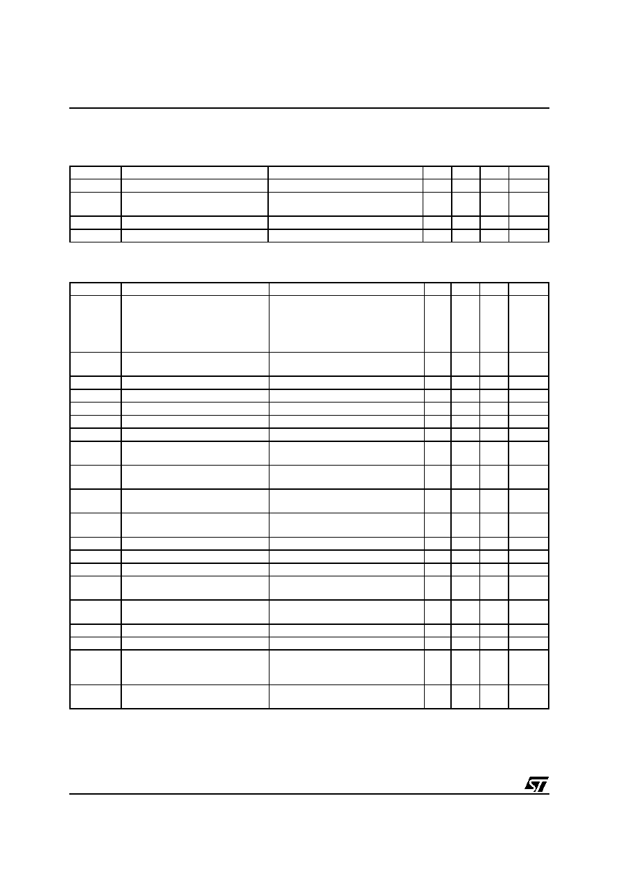
STV223XD/224XC - ELECTRICAL CHARACTERISTICS
24/76
Note 1: Additional sinked current for large increasing steps of input signal when:
- Voltage at PIFinput > Tuner AGC starting point adjustment given by the WR03(d5 to d0)
- Output Signal (IntCVBSout) saturated (VIntCBVSoutVwth) in positive modulation.
SYNCHRONOUS VIDEO DEMODULATOR
Note 2: This parameter is not tested during production, it is tested during the qualification phase.
DEMODULATED VIDEO OUTPUT (INTCVBSOUT PIN)
Note 3: S/N = 20 log [PIFOUT Black to White / V
NOISE
(mV
RMS
) weighted CCIR 567.
Note 4: Supply Voltage ripple rejection = 20log (V
SUPPLY/
V
OUTPUT
) measured at 100 Hz with V
AC
Max. = 100 mVpp applied
to V
CC IF
= 5 V.
Symbol
Parameter
Test Conditions
Min.
Typ
Max.
Unit
DFPC
Vision Carrier Capture Range
±2
MHz
f
VCO
Maximum VCO Frequency for PIF
regeneration
With external LC network at 50 MHz
(see Note 2)
50
MHz
V
ILOCK
PIF Input Signal for PIF PLL locking
40
70
µV
RMS
TVCO
PIFVCO Temperature Coefficient
±20
ppm/K
Symbol
Parameter
Test Conditions
Min.
Typ
Max.
Unit
PIFOUT-Q
PIFOUT-I
Video Amplitude at INTCVBSOUT
Pin
Black-to-White Video amplitude:
reg 02 data = 10h
(INTCVBSOUT =2 V
PP
)
reg 02 data = 90h
(INTCVBSOUT =2.3 V
PP
)
1.19
1.36
1.4
1.6
1.61
1.84
V
BG/L
BG to L Ratio
Video amplitude bus register
Typ.: reg 02 data = 10 hex
5
8
%
DG
Differential Gain
3
5
%
DP
Differential Phase
3
5
deg
V
PIF
Residual Carrier Signal
1
10
mV
RMS
V
R2IF
Residual 2nd Harmonic
1
10
mV
RMS
S/N
Video Output S/N Ratio
See Note 3
55
60
dB
V
WTH
White Noise Threshold Voltage
reg 02 data = 90h
2.3 V
PP
at INTCVBSOUT Pin
6.7
V
V
WIL
White Noise Insertion Level
reg 02 data = 90h
2.3 V
PP
at INTCVBSOUT Pin
3.7
V
V
BTH
Black Noise Threshold Voltage
reg 02 data = 90h
2.3 V
PP
at INTCVBSOUT Pin
1
V
V
BIL
Black Noise Insertion Level
reg 02 data = 90h
2.3 V
PP
at INTCVBSOUT Pin
2.6
V
BW
Video Bandwidth
6
8
10
MHz
LUMLIN
Luminance Non Linearity
5
%
ROUT
Internal Output Resistance
50
RLOAD
Output Load Resistance
reg 02 data = 10hex
(INTCVBOUT = 2 V
PP
)
2
3
k
IVID
Video Output Source Current
reg 02 data = 90hex
(INTCVBSOUT = 2.3 V
PP
)
7
10
13
mA
DCOUT
DC Output Level
Top Sync Level
2
V
Inter Mod.
1.07 MHz Intermodulation
Intercarrier Mode
52
dB
PSRR
Power Supply Ripple Rejection
Video signal Grey level (see Note 4)
BG standard
L standard
35
30
dB
NH
Suppression of Video signals har-
monics
35
40
dB
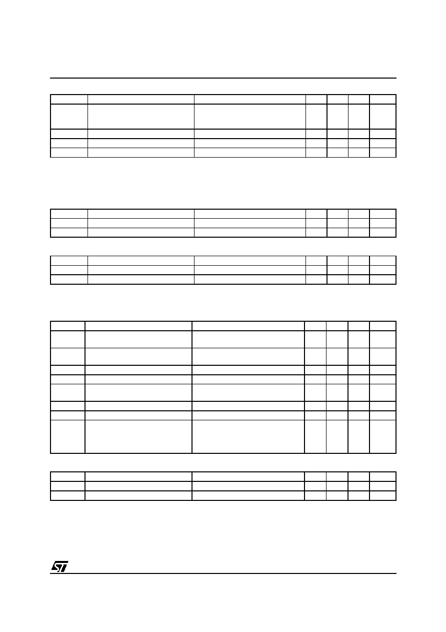
STV223XD/224XC - ELECTRICAL CHARACTERISTICS
25/76
SIF AMPLIFIER
Note 5: L standard Sc/Pc = -10 dB, Nyquist Pc = -6 dB, SIF input -4 dB with PIF input = 84 µV, BG standard Sc/Pc = -
13 dB, Nyquist Pc = -6 dB, SIF input -7 dB with PIF input = 85 µV.
Note 6: This parameter is not tested during production. It is tested on the validation bench during the qualification phase.
SIF AGC (FM)
SIF AGC (AM)
DEEMPHASIS
Symbol
Parameter
Test Conditions
Min.
Typ
Max.
Unit
VINSIF
SIF Input Sensitivity
- 3dB at AM/FMOUT Pin (see Note 5)
AM output amplitude,
FM subcarrier amplitude
55
40
µV
RMS
GRSIF
Gain Control Range
- 3dB to +1dB at AM/FMOUT Pin
60
dB
C
INSIF
Differential Input Capacitance
SIF Inputs (see Note 6)
1.5
2
2.5
pF
R
INSIF
Differential Input Resistance
SIF Inputs
1.5
2
2.5
k
Symbol
Parameter
Test Conditions
Min.
Typ
Max.
Unit
I
C
Charging Current
2.4
mA
I
D
Discharging Current
100
µA
Symbol
Parameter
Test Conditions
Min.
Typ
Max.
Unit
I
NORMAL
Charging/Discharging Current
Normal time constant
±6
µA
I
FAST
Charging/Discharging Current
Fast time constant
±2.4
mA
FM DEMODULATOR
Electrical parameter valid in both QSS and Intercarrier modes, unless otherwise specified.
Symbol
Parameter
Test Conditions
Min.
Typ
Max.
Unit
SIFMin
Min. Broadcast Sound/Video Carri-
er Ratio
Intercarrier mode: SAW filter K2955M
at SNR 35 dB
-30
dB
VOAF
FM Audio Output Amplitude at AM/
FMOUT Pin
FM dev = ±27kHz BGDKI
FM dev = ±13.5kHz MN
400
500
630
mV
RMS
DFMX
Maximum FM Deviation
THD < 10%
170
kHz
THD_FM
Total Harmonic Distortion
FM dev = ±27kHz BGDKI
0.3
1
%
S/N
Audio S/N
Weighted according to CCIR468-4
Quasi-Peak
55
dB
AMR
Amplitude Modulation Rejection
m = 30%, AF = 1 kHz
32
dB
SVR
Supply Voltage Rejection
See Note 4
45
dB
S/N
vsvideo
S/N versus picture content, Inter-
carrier mode
Intercarrier mode: SAW filter K2955M
Black picture,
White picture,
250 kHz squarewave
52
50
52
dB
Symbol
Parameter
Test Conditions
Min.
Typ
Max.
Unit
deemp-T1 De-emphasis Time Constant
B,G,D,K,I standards
50
µs
deemp-T2 De-emphasis Time Constant
M, N, standards
75
µs
STV223XD/224XC - ELECTRICAL CHARACTERISTICS
26/76
AM DEMODULATOR
SIF OUTPUT (AM/FM OR SOUND SUBCARRIERS OUTPUT)
SAW FILTER SWITCH OUTPUT
EXTERNAL AUDIO INPUT
MAIN AUDIO OUTPUT
(See
Figure 17
and
Figure 18
)
Symbol
Parameter
Test Conditions
Min.
Typ
Max.
Unit
AFOUT
AM Audio Output Amplitude at AM/
FMOUT Pin
54% modulation
400
500
630
mV
RMS
AMlowco
Low Cut-off Frequency
-3 dB compared AFout
40
Hz
AMhighco
High Cut-off Frequency
-3 dB compared AFout
30
kHz
AMthd
Total Harmonic Distortion
54% modulation
2
%
AMs/n
Signal/Noise Ratio
Weighted according to CCIR468-4
Quasi-Peak
55
dB
AMsvr
Supply Voltage Rejection
See Note 4
20
dB
Symbol
Parameter
Test Conditions
Min.
Typ
Max.
Unit
SIFout
Output Level
Sound subcarriers
150
mV
RMS
SIFbw
Bandwidth
Sound subcarriers
7.5
MHz
SIF dcout
DC Output Level
4
V
SIFres
Residual Carrier
Fundamental wave (38.9 MHz) and
harmonics
0.4
mV
RMS
SIFcur
Sink Output Current
AM or FM demod. output selected
Sound subcarriers output selected
0.5
1.5
mA
Symbol
Parameter
Test Conditions
Min.
Typ
Max.
Unit
SAW low
Low Output Voltage
I
SINK
= 2 mA
0.4
V
SAWcur
Maximum allowed Current
2
mA
SAW high
High Output Voltage
I
SOURCE
= 2 mA
4
V
Symbol
Parameter
Test Conditions
Min.
Typ
Max.
Unit
R
IN
Input Resistance
70
100
130
k
V
IDC
DC Input Voltage
2.4
V
AFIN
maximum Audio Input Signal
2
V
RMS
Symbol
Parameter
Test Conditions
Min.
Typ
Max.
Unit
AMax
Maximum Attenuation (Audio Out/
AM-FM Out)
Register 05hex, data = 7Fhex
78
dB
AMin
Minimum Attenuation (Audio Out/
AM-FM Out)
V
IN
= 1 V
RMS,
f = 1 kHz,
Register 05hex, data = 00hex
-1
0
1
dB
ASTEP
Step Resolution
reg 05, d7 = 0
0.7
dB
DCSH
DC Output Shift
From max. volume to min. volume
50
mV
V
ODC
DC Output Level
4
V
AFDIFF
Audio Amplitude difference
between sources
f = 1 kHz, f
M
= ±27 kHz,
Ext. Audio Input = 500 mV
RMS
2
dB
R
OUT
Output Resistance
110
BWO
Output Bandwidth
1
MHz
THD_AM
Total Harmonic Distortion
V
IN
= 1 V
RMS,
f = 1 kHz
0.1
0.3
%
S/N1
Signal to Noise Ratio from Exter-
nal Input
Measured at 0 dB attenuation,
Ext. Audio Input at 500 mV
RMS,
CCIR 468-4 Weighted Quasi Peak
75
dB
STV223XD/224XC - ELECTRICAL CHARACTERISTICS
27/76
Note 7: Measured from any input to output at f = 10 kHz with RL = 10k
and Rg = 600
, Volume attenuation = 0dB.
AVL
4.5 CVBS, Y/C, RGB INPUTS AND CVBS OUTPUTS
LUMINANCE AND CVBS INPUTS
COMBINED CHROMINANCE AND SVHS SELECTION INPUT
CVBS1 OUTPUT
S/N2
Signal to Noise Ratio from Exter-
nal Input
Measured at 20 dB attenuation,
0 dB reference
Ext. Audio Input at 500 mV
RMS
55
60
dB
S/N3
Signal to Noise Ratio from FM
Demod
Measured at 20 dB attenuation,
FM: ± 27 kHz (Standards BGDKI)
52
55
dB
SVRV
Supply Voltage Rejection from
External Input
Measured at f = 100 Hz from
V
CC
= 5 V and V
CC
= 8 V
60
dB
XT
Crosstalk
See Note 7
70
dB
NOISE
Output Noise Level
CCIR 468-4 Weighted Quasi Peak
Volume at minimum
Volume at typical
Volume at maximum
50
50
100
60
60
120
µV
AFIN
Audio Input Level
Volume = -25 dB, THD < 1%
2
V
RMS
Symbol
Parameter
Test Conditions
Min.
Typ
Max.
Unit
Symbol
Parameter
Test Conditions
Min.
Typ.
Max.
Unit
GAVL
AVL Gain Control Range
(7-bit Resolution)
20
dB
AVL
MAX
Maximum attenuation
-15
dB
Reg.AVL
Regulation amplitude
Measured at AUDIOOUT
Volume Control at maximum
0.55
V
RMS
Symbol
Parameter
Test Conditions
Min.
Typ
Max.
Unit
DC
IN1
Black Level Voltage
Input selected on main CVBS output
3.3
V
V
IN
CVBS or Y Input Voltage
1
1.41
V
PP
-I
Negative Clamping Current
During SYNC pulse
20
27
35
µA
I
Positive Clamping Current
2.5
4.5
7
µA
Symbol
Parameter
Test Conditions
Min.
Typ
Max.
Unit
V
Chrominance Input Voltage
Burst Amplitude, 100/75 Color Bar
0.3
0.6
V
PP
V
CLIP
Input Amplitude before Clipping
1
V
PP
V
DC
DC Voltage
SVHS Mode
1.55
1.70
1.85
V
V
TH
SVHS Threshold Voltage
0.50
0.90
1.45
V
I
LOW
Output Current
0V at CHR Pin
150
µA
Symbol
Parameter
Test Conditions
Min.
Typ
Max.
Unit
V
OUT
Dynamic Output Amplitude
1.5
V
PP
R
OUT
Internal Output Resistance
50
R
LOAD
Output Load Resistance
1.5
k
BW
CVBS Bandwidth
V
IN
= 1V
PP
10
MHz
Crosstalk
Deletion of non-selected signals
Up to 5 MHz
50
dB
MGAIN
Output Gain
From any CVBS/Y inputs
-0.5
0
0.5
dB
DCMAIN
DC Output Voltage
Black Level
3.5
V
STV223XD/224XC - ELECTRICAL CHARACTERISTICS
28/76
CVBS1 OUTPUT (Pin 29 - SDIP56)
CVBS2 OUTPUT
OSD RGB INPUTS
OSD FAST BLANKING INPUT (TQFP64)
Symbol
Parameter
Test Conditions
Min.
Typ
Max.
Unit
V
OUT
Dynamic Output Amplitude
Register 1Dhex, data = 07hex
1.5
V
PP
R
LOAD
Output Load Resistance
Register 1Dhex, data = 07hex
3
k
BW
CVBS Bandwidth
Register 1Dhex, data = 07hex
V
IN
= 1V
PP
10
MHz
Crosstalk
Deletion of non-selected signals
Register 1Dhex, data = 07hex
Up to 5 MHz
50
dB
MGAIN
Output Gain
Register 1Dhex, data = 07hex
From any CVBS/Y inputs
-0.5
0
0.5
dB
DCMAIN
DC Output Voltage
Register 1Dhex, data = 07hex
Black Level
4.2
V
Symbol
Parameter
Test Conditions
Min.
Typ
Max.
Unit
V
OUT2
Dynamic Output Amplitude
3
V
PP
R
OUT2
Internal Output Resistance
10
BW2
CVBS Bandwidth
V
IN =
1 V
PP
10
MHz
Crosstalk2 Deletion of non-selected signals
Up to 5 MHz
50
dB
SWI2gain
Output Gain
From any CVBS/Y inputs
5.5
6
6.5
dB
SWI2DC
DC Output Voltage
Black Level
3.8
V
R
LOAD2
Output Load Resistance
1.5
k
Symbol
Parameter
Test Conditions
Min.
Typ
Max.
Unit
V
CLAMP
Clamp Level
Max. Contrast
4
V
V
RGB
RGB Input Voltage
0.7
1
V
PP
CRGB
RGB Gain
Max. Contrast, Max. Drive
4.28
-
Dblack
Difference of black level of internal
and external signals at the RGB out-
puts
OSD signal versus internal signal
50
mV
I
RGB
Clamping Current
60
100
140
µA
Crosstalk
Deletion of non-selected RGB source From 0 to 5 MHz
50
dB
Symbol
Parameter
Test Conditions
Min.
Typ
Max.
Unit
V
THFB1
Insertion Threshold Voltage
0.5
0.7
0.85
V
V
THFB2
Blanking Threshold Voltage,
Oversize Blanking active
Register 08hex d7 = 1
3.2
4
4.8
V
t
SWI1
Insertion Switching Delay
20
40
ns
t
SWI2
Blanking Switching Delay
From FBOSD = 4V to starting of
blanking falling edge at RGB out-
puts
100
ns
I
FB
Input current
0V at Pin FBOSD
10
µA
STV223XD/224XC - ELECTRICAL CHARACTERISTICS
29/76
HALF CONTRAST INPUT (TQFP64)
FBOSD/HC INPUTS (SDIP56)
EXTERNAL RGB/YCrCb INPUTS
EXTERNAL FAST BLANKING INPUT (See Note 8)
Note 8: FBEXT input must be connected to ground if not used in the application.
Symbol
Parameter
Test Conditions
Min.
Typ
Max.
Unit
V
TH_HC
Half Contrast Threshold Voltage
0.5
0.7
0.85
V
tsWI_HC Half Contrast Delay
20
ns
CTR_HC
Contrast Attenuation when half con-
trast active
At Max. Contrast
6
dB
I_HC
Leakage Current
0V at Pin HC
10
µA
Symbol
Parameter
Test Conditions
Min.
Typ
Max.
Unit
V
THFB1A
OSD Insertion Threshold Voltage
Half Contrast disable
Register 08hex d6 = 0
0.5
0.7
0.85
V
V
THFB1B
OSD Insertion Threshold Voltage
Half Contrast enable
Register 08hex d6 = 1
1.5
1.9
2.3
V
V
TH-HC
Half Contrast Threshold Voltage
Half Contrast enable
Register 08hex d6 = 1
0.5
0.7
0.85
V
V
THFB2
Blanking Threshold Voltage,
Oversize Blanking active
Register 08hex, d7 = 1
3.2
4
4.8
V
t
SWI1
Insertion Switching Delay
20
40
ns
t
SWI2
Blanking Switching Delay
From FBOSD = 4V to starting of
blanking falling edge at R,G,B out-
puts
100
ns
I
FB
Input current
0V at Pin FBOSD
10
µA
Symbol
Parameter
Test Conditions
Min.
Typ
Max.
Unit
V
CLAMP
Clamp Level
Max. Contrast
3.5
V
V
RGB
RGB Input Voltage
0.7
1
V
PP
V
YCrCb
YCrCb Input Voltage
100% color bar
register 0Ahex d7d6 = 11
Y
Cr
Cb
1
0.7
0.7
V
PP
CRGB
RGB Gain
Max. Contrast, Max. Drive
4.28
-
Dblack
Difference of black level of internal
and external signals at the RGB out-
puts
OSD signal versus internal signal
50
mV
I
RGB
Clamping Current
60
100
140
µA
Crosstalk Deletion of non-selected RGB source From 0 to 5 MHz
50
dB
Symbol
Parameter
Test Conditions
Min.
Typ
Max.
Unit
V
THFB
Insertion Threshold Voltage
0.5
0.7
0.85
V
t
SWI
Insertion Switching Delay
20
40
ns
I
FB
Input Current
0V at Pin FBEXT
10
µA
V
MAX
Max. voltage allowed at FBEXT input
5
V

STV223XD/224XC - ELECTRICAL CHARACTERISTICS
30/76
4.6 LUMA PART
Y
DELAY LINE
PEAKING CIRCUIT
Electrical parameter measured with color identified
BLACK STRETCH CONTROL (PIN BS) See
Figure 12
Y OUTPUT
Symbol
Parameter
Test Conditions
Min.
Typ
Max.
Unit
t
D1
Delay Time PAL/NTSC
SVHS mode, Register 1F d3 = 0
520
ns
t
D2
Delay Time SECAM
SVHS mode, Register 1F d3 = 0
640
ns
t
D3
Delay Time PAL/NTSC
CVBS mode, Register 1F d3 = 0
560
ns
t
D4
Delay Time SECAM
CVBS mode, Register 1F d3 = 0
710
ns
t
SHIFT
Delay Time (lumDel1 - lumDel2)
lumDel1 = reg 1F d3 = 0, standard
luma delay
lumDel2 = reg 1F d3 = 1, shifted luma
delay
140
ns
Groupdel
Group Delay up to 3.5MHz
Trap-off
±30
ns
Symbol
Parameter
Test Conditions
Min.
Typ
Max.
Unit
fPEAK
Center Frequency
Trap-off, coring ON
2.5
3
3.5
MHz
G
PEAK
Gain Variation from Min. to Max.
peaking
At f
PEAK
, coring ON
9
dB
Overshoot
Amplitude Variation compared to
B/W amplitude
2T pulse, Max. peaking, coring ON
55
%
Pre-shoot
Amplitude Variation compared to
B/W amplitude
2T pulse, Max. peaking, coring ON
40
%
Aft-shoot
Amplitude Variation compared to
B/W amplitude
2T pulse, Max. peaking, coring ON
40
%
Coring
Coring Range compared to B/W
Coring ON
10
%
Symbol
Parameter
Test Conditions
Min.
Typ
Max.
Unit
BSth1
Black Stretch Threshold referred to
B/W amplitude
Y/CVBS inputs: 0.7V B/W, No set-up
50
%
BSMax.
Maximum expansion referred to
B/W amplitude
Y/CVBS inputs: 0.7V B/W, No set-up
-20
%
BSVMax. Black Stretch Control Voltage
Max. black stretch
2.6
V
BSVMin.
Black Stretch Control Voltage
No black stretch
3.3
V
I100IRE
Discharging current
Y = 100IRE
8
µA
I0IRE
Charging Current
Y = 0IRE
35
µA
Symbol
Parameter
Test Conditions
Min.
Typ
Max.
Unit
Yout-DC
Black level
3.7
VBW
Yout-amp Black to White Amplitude
0.7
0.99
V
Yout-BW Luma Path Bandwidth
Peaking nominal
SVHS mode/Trap-off
CVBS, PAL/NTSC 4.43MHz
CVBS, SECAM
CVBS, PAL/NTSC 3.58MHz
8
2.7
2.5
2.5
3.5
3.1
3.0
MHz
Yout S/N Signal to Noise Ratio (V
PP
/V
RMS
)
Bandwidth 5MHz,
Peaking Min.,coring ON
50
dB
STV223XD/224XC - ELECTRICAL CHARACTERISTICS
31/76
4.7 FILTERS
Y TRAP FILTER
CHROMINANCE BANDPASS
CLOCHE FILTER
4.8 CHROMA PART
Symbol
Parameter
Test Conditions
Min.
Typ
Max.
Unit
f
TRAP-PN
Notch Frequency
PAL/NTSC
f
OSC
MHz
f
TRAP-S
Notch Frequencies
SECAM fnb
SECAM fnr
4.2
4.5
MHz
f
TRAP-ACC
Notch Frequency Accuracy
3.5
%
Q
TRAP
Trap Quality Factor
Q = 1/ (f0/f-3dB - f-3dB/f0), Peaking
Min.
1.5
-
CrejPN
Color Subcarrier Rejection
PAL/NTSC
20
dB
CrejS
Color Rejection in SECAM Mode
From 4.1 to 4.6 MHz
At 3.9 MHz
10
20
dB
Symbol
Parameter
Test Conditions
Min.
Typ
Max.
Unit
f
BP
Center Frequency
Register 12h, d3-d0 = 0000
-5%
f
OSC
+5%
MHz
Q
BP
Bandpass Quality Factor
2.8
3.5
4.2
-
Symbol
Parameter
Test Conditions
Min.
Typ
Max.
Unit
f
CLOCHE
Center Frequency
Register 11h, d4-d0 = 00000
4.27
4.29
4.31
MHz
Q
BP
Cloche Quality Factor
14
16
18
-
ACC
Symbol
Parameter
Test Conditions
Min.
Typ
Max.
Unit
G
ACC
ACC Control Range
Change of burst overall ACC control
range < 2dB
26
dB
V
Min.
Minimum Burst Signal Amplitude
Within the ACC control range
0.03
V
PP
ACC OVERLOAD
Symbol
Parameter
Test Conditions
Min.
Typ
Max.
Unit
V
TH
Chroma regulation Threshold
ACC overload ON, PAL/NTSC
3
dB
KILLER
Symbol
Parameter
Test Conditions
Min.
Typ
Max.
Unit
Ident-kill
Color on Threshold of ident. circuit
Burst amplitude on selected CVBS
input
5
mV
PP
Kill-Hyst
Color off Killer Hysteresis
Strong signal condition, S/N > 40 dB
2
mV
PP
CHROMA PLL
Symbol
Parameter
Test Conditions
Min.
Typ
Max.
Unit
CaptR
Catching Range
With recommended crystal and rec-
ommended CLPF filter value.
±300
HoldR
Holding Range
> or = to capture range
STV223XD/224XC - ELECTRICAL CHARACTERISTICS
32/76
COLOR DEMODULATORS
CHROMA DELAY LINE
PLL LOOP FILTER (PAL/NTSC)
Symbol
Parameter
Test Conditions
Min.
Typ
Max.
Unit
I
C
Maximum Control Current
Color search mode (colour not ident.)
Color identified
1000
350
µA
I
L
Leakage Current
5
µA
Frange-W
Auto Flesh Control
Register 14(HEX), d6 = 1, d7 = 1
±90
Deg
HUE CONTROL
Symbol
Parameter
Test Conditions
Min.
Typ
Max.
Unit
Rhue
Hue Control Range
±35
±45
±55
Deg
AUTOMATIC FLESH CONTROL See
Figure 13
Symbol
Parameter
Test Conditions
Min.
Typ
Max.
Unit
FleshNom. Nominal Flesh tint phase
118
Deg
Fcorr0
Phase Correction when auto flesh
ON
At FleshNom
0
Deg
FMax.-N
Maximum Phase Correction
Register 14(HEX), d6 = 1, d7 = 0
±10
Deg
Flesh-N
Chroma Input Phase at Max. cor-
rection
Register 14(HEX), d6 = 1, d7 = 0
±30
Deg
Frange-N
Auto Flesh Control Range
Register 14(HEX), d6 = 1, d7 = 0
±60
Deg
FMax.-W
Maximum Phase Correction
Register 14(HEX), d6 = 1, d7 = 1
±20
Deg
Flesh-W
Chroma Input Phase at Max. cor-
rection
Register 14(HEX), d6 = 1, d7 = 1
±45
Deg
Frange-W
Auto Flesh Control
Register 14(HEX), d6 = 1, d7 = 1
±90
Deg
Symbol
Parameter
Test Conditions
Min.
Typ
Max.
Unit
DoffsetP
Demodulator Offset
PAL/NTSC mode, 75% color bar
±2
%
DoffsetS
Demodulator Offset
SECAM mode, 75% color bar
±2
%
PhaseErr
Phase Error in demodulated signal
PAL/NTSC mode, 90% matrix
5
Deg
TransPal
Chroma Transient Time
PAL mode, 75% color bar green-
magenta transient
700
ns
transSEC
Chroma Transient Time
SECAM mode, 75% color bar green-
magenta transient
900
ns
Naxis
R-Y Demodulation Axis
NTSC mode, 104∞ matrix
104
Deg
Symbol
Parameter
Test Conditions
Min.
Typ
Max.
Unit
Cdelay
Delay of delayed signals
Relative to non delayed signal
63.9
64
64.1
µs
Ctrans
Difference of transient times be-
tween delayed and non delayed
signals
SECAM mode. t
RN
-t
RN+1
t
RN
: rise time line N (direct)
t
RN+1
: rise time line N +1 (delayed)
150
ns
Dgain
Differential Gain of delayed signals
versus direct signals
SECAM mode. Gn+1/Gn
Gn: direct channel gain
Gn+1: delayed channel gain
-0.5
0
0.5
dB
STV223XD/224XC - ELECTRICAL CHARACTERISTICS
33/76
U & V OUTPUTS (TQFP64)
CHROMA REFERENCE OUTPUT
4.9 SCANNING PART
SYNC. SEPARATOR
HORIZONTAL OSCILLATOR
FIRST LOOP FILTER
SECOND LOOP FILTER
Symbol
Parameter
Test Conditions
Min.
Typ
Max.
Unit
UVout-dcc Black Level
3.7
V
Uout-amp
B-Y Signal Amplitude
Chroma delay line ON,
75% color bar PAL/SECAM
1.33
V
PP
Vout-amp
R-Y Signal Amplitude
Chroma delay line ON,
75% color bar PAL/SECAM
1.05
V
PP
UVres
Internal Output Resistance
300
Uout-amp
B-Y Signal Amplitude
Chroma delay line OFF,
75% color bar PAL
0.66
V
PP
Vout-amp
R-Y Signal Amplitude
Chroma delay line OFF,
75% color bar PAL
0.52
V
PP
DemRatio
Ratio of B-Y/R-Y demodulators
gain
75% color bar PAL/SECAM,
measured on U, V outputs
1.14
1.27
1.4
-
RES
Residual Subcarrier at U, V outputs
45
mV
PP
Lum/chr
Luma/Chroma Delay Difference at
U, V outputs
External CVBS input signal,
reg 1Fd3 = 0
±80
ns
Symbol
Parameter
Test Conditions
Min.
Typ
Max.
Unit
CHR-amp
Chroma VCO Reference Signal
Amplitude
0.4
V
PP
I
SCHR
Sink Current
0.5
mA
Symbol
Parameter
Test Conditions
Min.
Typ
Max.
Unit
Vsync
Synchronization Pulse Amplitude
50
300
450
mV
Symbol
Parameter
Test Conditions
Min.
Typ
Max.
Unit
f
H50
Horizontal Frequency
50 Hz mode
15.6
kHz
f
H60
Horizontal Frequency
60 Hz mode
15.7
kHz
f
RANGE
Frequency Control Range
Low Frequency
High Frequency
14.7
15.9
15.0
16.3
15.3
--
kHz
f
FREE
Free Frequency when PLL1 opened
15.3
15.6
15.9
kHz
Symbol
Parameter
Test Conditions
Min.
Typ
Max.
Unit
I
LOW
Long Time Constant Output Current
0.10
0.13
0.16
mA
I
HIGH
Short Time Constant Output Current
0.30
0.40
0.56
mA
I
VLOW
Very Long Time Constant
0.03
0.05
0.07
mA
Symbol
Parameter
Test Conditions
Min.
Typ
Max.
Unit
CrangeP2
Control Range from start of horizon-
tal output to flyback pulse
Centered horizontal position
0 to
12
µs
Hshift
Horizontal Position Control Range
5
5.25
µs
Hdrift
Horizontal Drift with temperature
From 0∞C to 70∞C (see Note 9)
200
ns
STV223XD/224XC - ELECTRICAL CHARACTERISTICS
34/76
Note 9: This parameter is not tested during production, it is tested during qualification phase.
LINE FLYBACK INPUT/SUPER-SANDCASTLE OUTPUT
HORIZONTAL OUTPUT
VERTICAL OUTPUT
VERTICAL AMPLITUDE CONTROL
CRYSTAL DETECTION
Symbol
Parameter
Test Conditions
Min.
Typ
Max.
Unit
V
BURST
Output Voltage during Burst Key
4.8
5.3
5.8
V
V
LINE
Clamped Input Voltage during Line
Flyback
2.6
3
3.4
V
V
VERT
Output Voltage during Vertical pulse
1.8
2
2.2
V
Twbg
Burst key Pulse Width
3.8
µs
Tdbg
Delay of start of burst key to start of
sync.
5.2
µs
Tvert
Vertical Pulse Width
10.5
lines
V
THLINE
PLL2 and Line Blanking Threshold
Voltage referred to line level Vline
Vthline/Vline
83
%
I
Input Current
0.1
1
mA
Symbol
Parameter
Test Conditions
Min.
Typ
Max.
Unit
t
W
Output Pulse Width
26
28
30
µs
V
LOW
Low Output Voltage
I
SINK
= 5mA
0.4
V
V
CCSTART
V
CC
Start Level
5.5
6
6.5
V
V
CCSTOP
V
CC
Stop Level Hysteresis
V
CCSTART
- V
CCSTOP
0.5
0.6
0.7
V
I
Max.
Maximum allowed Output Current
10
mA
V
Max.
Maximum allowed Output Voltage
10
V
Tss
Output Pulse Duty Cycle in soft-start
mode (t
HIGH
/(t
HIGH
+t
LOW
)
75
%
Symbol
Parameter
Test Conditions
Min.
Typ.
Max.
Unit
t
W
Output Pulse Width
10.5
Lines
V
LOW
Low Output Voltage
4/3 selected, reg 19, d0 = 1
16/9 selected, reg 19, d0 = 0
1.5
2
0.1
2.5
0.5
V
f
LOCK
Looking Range
248
352
Lines
f
FREE-50
Free Frequency (no Video signal)
50-Hz Forced or 50-Hz Auto mode
314
Lines
f
FREE-60
Free Frequency (no Video signal)
60-Hz Forced or 60-Hz Auto mode
264
Lines
V
HIGH
High Level Range Vertical Position
Control
Min. position control
Max. position control
3.5
6.0
4
6.5
4.5
7.0
V
I
SINK
Output Sinking Current
0.7
1.0
mA
I
SOURCE
Output Source Current
0.7
1.0
mA
Symbol
Parameter
Test Conditions
Min.
Typ.
Max.
Unit
V
AMP
Output Voltage Range
Min. amplitude voltage
Max. amplitude voltage
1.2
5.5
1.5
6.0
1.7
6.5
V
Symbol
Parameter
Test Conditions
Min.
Typ.
Max.
Unit
R
4.43
Load resistance at pin VAMP
4.43 MHz crystal on pin XTAL1
80
k
R
3.58
Load resistance at pin VAMP
3.58 MHz crystal on pin XTAL1
10
k
STV223XD/224XC - ELECTRICAL CHARACTERISTICS
35/76
4.10 RGB CONTROL PART
Y INPUT
Symbol
Parameter
Test Conditions
Min.
Typ
Max.
Unit
YINdc
Black Level
3.7
V
Yin-B/W
Black to White Amplitude
0.7
1
V
Yin-cur
Input Current
1
µA
U & V INPUTS
Symbol
Parameter
Test Conditions
Min.
Typ
Max.
Unit
UVin-dc
Black Level
3.7
V
Uin-amp
B-Y Amplitude
75% color bar PAL/SECAM
1.33
2.0
V
PP
Vin-amp
R-Y Amplitude
75% color bar PAL/SECAM
1.05
2.0
V
PP
UVin-cur
Input Current
1
µA
CONTRAST CONTROL
Symbol
Parameter
Test Conditions
Min.
Typ
Max.
Unit
Yctr
Contrast Range on Y signal
21
24
27
dB
OSDctr
Contrast Range on OSD RGB sig-
nal
10
12
14
dB
SATURATION CONTROL
Symbol
Parameter
Test Conditions
Min.
Typ
Max.
Unit
SAT
Max.
Maximum Saturation Control
75% color bar PAL/SECAM,
0 dB for data 20 in reg 08
6
9
12
dB
SAT
Min.
Minimum Saturation Control
75% color bar PAL/SECAM,
0 dB for data 20 in reg 08
-40
dB
BRIGHTNESS CONTROL
Symbol
Parameter
Test Conditions
Min.
Typ
Max.
Unit
Bright
Brightness Control Range referred
to B/W amplitude on RGB outputs
At Max. Contrast
50
60
70
%
Blacknom
Nominal Black Level at RGB out-
puts. Difference between black lev-
el V
BLACK
and inserted cut-off pulse
level V
CO
: V
BLACK
- V
CO
BS mode, Max. Contrast.
(V
BLACK
- V
CO
)/V_BW
V_BW: black to white amplitude at
RGB outputs.
-12
%
RGB MATRIX
Symbol
Parameter
Test Conditions
Min.
Typ
Max.
Unit
G/R
(G-Y)/(R-Y)
PAL/SECAM matrix measured on R,
G outputs PAL DEMpattern
-0.40
-0.51
-0.62
-
G/B
(G-Y)/(B-Y)
PAL/SECAM matrix measured on G,
B outputs PAL DEMpattern
-0.15
-0.19
-0.23
-
R/Bntsc
(R-Y)/(B-Y)
NTSC mode, 104∞ matrix input signal:
U = V measured on R, B outputs
0.9
-
G/Rntsc
(G-Y)/(R-Y)
NTSC mode, 104∞ matrix
-0.29
-
G/Bntsc
(G-Y)/(B-Y)
NTSC mode, 104∞ matrix
-0.22
-
STV223XD/224XC - ELECTRICAL CHARACTERISTICS
36/76
DRIVE ADJUSTMENT (WHITE POINT ADJUSTMENT)
Symbol
Parameter
Test Conditions
Min.
Typ
Max.
Unit
WPrange
White Point Adjustment Range
On RGB outputs
6
dB
CUT-OFF ADJUSTMENT (BLACK POINT ADJUSTMENT)
Symbol
Parameter
Test Conditions
Min.
Typ
Max.
Unit
COadjust
Cut-off Adjustment Range
On Red and green outputs at Typ.
drive, no load
420
mV
COloop
Cut-off Loop Range
On RGB outputs
2
2.5
V
COlevel
Inserted Cut-off Level
1.5
2.5
3.5
V
CATHODE CURRENT INPUT
Symbol
Parameter
Test Conditions
Min.
Typ
Max.
Unit
V
LEAK
Leakage Current Reference Volt-
age
3.75
4
V
V
COFF
Cut-off Current Reference Voltage
referred to leakage current refer-
ence V
LEAK
210
250
290
mV
V
SBEAM
Start Beam Current Detection Ref-
erence Voltage
4.1
4.3
V
I
SOURCE
Source Current
150
µA
BEAM CURRENT LIMITER INPUT See
Figure 14
and
Figure 15
Symbol
Parameter
Test Conditions
Min.
Typ
Max.
Unit
V
TH1
Contrast Attenuation Starting
5.75
V
V
TH2
Brightness Attenuation Starting
5.5
V
V
TH3
Contrast Attenuation Ending
5.25
V
CTRbcl
Contrast Attenuation at V
TH3
14
dB
V
TH4
Brightness Attenuation Ending
4.5
V
BRIGbcl
Brightness Attenuation at V
TH4
100
%
Clp
High Clamping Voltage
6.5
V
SAF-thr
Safety Threshold
0.8
1
1.2
V
SAF-hold
Supply Hold Voltage
Referred to V
CC1
3
V
AUTOMATIC RGB PEAK REGULATION See
Figure 16
Symbol
Parameter
Test Conditions
Min.
Typ
Max.
Unit
APR
Maximum Output Level on RGB
outputs when APR ON
Contrast Max., drive Max., no load
APR threshold Min. (50IRE)
APR threshold 70IRE
APR threshold Max. (100IRE)
2.14
3.0
4.28
V
i
APR-D
Discharging Current
5.5
µA
i
APR-C
Charging Current
5.25
mA
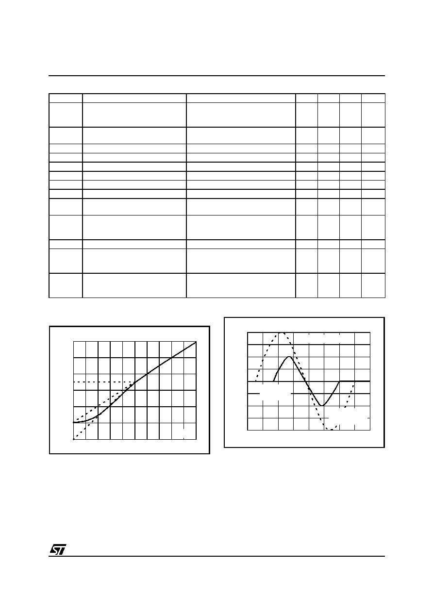
STV223XD/224XC - ELECTRICAL CHARACTERISTICS
37/76
Figure 12. Black Stretch Static Characteristics
(IRE)
Figure 13. Auto Flesh Characteristics
RGB OUTPUTS
Symbol
Parameter
Test Conditions
Min.
Typ
Max.
Unit
VB/W
Output Signal Amplitude B/W
0.7V B/W on Y/CVBS inputs, Contrast
Max., Drive Max., Saturation and
bright Nom., APR OFF, no load
3
V
V
BLUE
Output Signal Amplitude
75/100 color bar, no Y nom. settings,
APR OFF, no load
1.5
V
PP
I
SINK
Output Sinking Current
1.2
1.5
mA
I
SOURCE
Output Source Current
1.8
mA
R
OUT
Internal Output Resistance
150
V
BLANK
Blanking Level
No load
0.2
0.4
V
V
CLIP
High Clipping Level
No load
6.8
V
Black-ctr
Variation of black level with contrast
30
mV
Black-sat
Variation of black level with satura-
tion
50
mV
Rel-Black
Relative Variation in black level be-
tween the three channels
20dB contrast variation
Overall brightness range
±5% V
CC1
20
mV
Black-T
Black Level Thermal Drift
1
mV/∞C
Track
Tracking between Luminance and
Chrominance signals
At typical saturation
From Max. Contrast (0 dB) to -10 dB
Contrast
2
dB
Bwidth
Bandwidth of output signals at -3dB
YUV inputs to RGB outputs
OSD RGB inputs to RGB outputs
EXT. RGB inputs to RGB outputs
6
6
5
8
8
6
MHz
100
-20
0
50
50
100
YOUT
(%)
YIN (%)
-20
-10
0
10
20
Phase Correction (Deg)
0
90
210
240
60
150
30
120
180
Chroma Input
Phase (Deg)
Narrow
Response
Wide Response
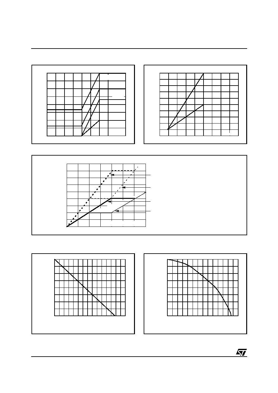
STV223XD/224XC - ELECTRICAL CHARACTERISTICS
38/76
Figure 14. Beam Current Limiter
Characteristics (Contrast)
Figure 15. Beam Current Limiter
Characteristics (Brightness)
Figure 16. APR Characteristics
Figure 17. Linear Volume Control Curve
(7 bits, reg. 05 d6-d0, reg. 05 d7 = 0)
Figure 18. Non-Linear Volume Control Curve
(6 bits, reg. 05 d6-d1, reg. 05 d7 = 1)
4.5
5
5.5
6
6.5
0
-12
-18
-24
-6
VBCL (V)
Contrast (dB)
-6dB
-10dB
-18dB
0dB Max.
4.5
5
5.5
6
6.5
0
50
100
VBCL (V)
Brightness (%)
0
50
100
150
Output Level
Input Level (IRE)
APR Threshold max. (100 IRE)
and contrast max.
APR Threshold min. (50 IRE)
and contrast max.
APR Threshold max. (100 IRE)
and contrast min.
APR Threshold min. (50 IRE)
and contrast min.
0
-20
-40
-60
-80
0
150
50
100
Code (decimal)
Volum
e Co
ntrol
Atten
uation
(dB)
0
-20
-40
-60
-80
0
10
70
Code (decimal)
Volu
me C
ontro
l Atte
nuatio
n (dB
)
30
50
20
40
60
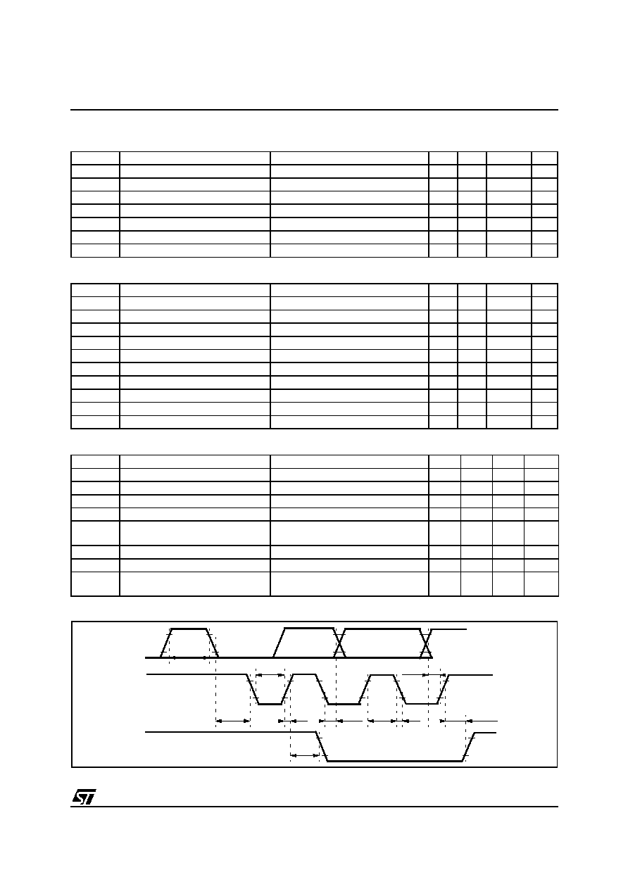
STV223XD/224XC - ELECTRICAL CHARACTERISTICS
39/76
4.11 I≤C BUS CHARACTERISTICS
SCL
SDA
I≤C TIMING
Figure 19. I≤C Bus Timing
Symbol
Parameter
Test Conditions
Min.
Typ
Max.
Unit
V
IL
Low Level Input Voltage
-0.5
1.5
V
V
IH
High
Level Input Voltage
3
V
CC
+0.5
V
I
LI
Input Leakage Current
V
IN
= 0 to V
CC
-10
10
µA
f
SCL
Clock Frequency
0
100
kHz
t
R
Input Rise Time
1.5V to 3V
1.000
ns
t
F
Input Fall Time
1.5V to 3V
300
ns
C
I
Input Capacitance
10
pF
Symbol
Parameter
Test Conditions
Min.
Typ
Max.
Unit
V
IL
Low Level input Voltage
-0.5
1.5
V
V
IH
High
Level input Voltage
3
V
CC
+0.5
V
I
LI
Input Leakage Current
V
IN
= 0 to V
CC
-10
10
µA
C
I
Input Capacitance
10
pF
t
R
Input Rise Time
1.5V to 3V
1.000
ns
t
F
Input Fall Time
1.5V to 3V
300
ns
V
OL
Low Level Output Voltage
I
OL
= 3mA
0.4
V
t
F
Output Fall Time
3V to 1.5V
250
ns
C
L
Load Capacitance
400
pF
C
I
Input Capacitance
10
pF
Symbol
Parameter
Test Conditions
Min.
Typ
Max.
Unit
t
LOW
Clock Low period
4.7
µs
t
HIGH
Clock High period
4
µs
t
SU,DAT
Data Set-up Time
250
ns
t
HD,DAT
Data Hold Time
0
340
ns
t
SU,STO
Set-up Time from Clock High to
Stop
4
µs
t
BUF
Start Set-up Time following a Stop
4.7
µs
t
HD,STA
Start Hold Time
4
µs
t
SU,STA
Start Set-up Time following Clock
Low to High Transition
4.7
µs
tBUF
tLOW
tHIGH
tHD,STA
tR
tF
tSU,STA
tHD,DAT
tSU,DAT
tSU,STO
SDA
SCL
SDA
STV223XD/224XC - I≤C BUS SPECIFICATIONS
40/76
5 I≤C BUS SPECIFICATIONS
Data transfers follow the usual I≤C format: after the
start condition (S), a 7-bit slave address is sent,
followed by an eight-bit which is a data direction bit
(W). An 8-bit sub-address is sent to select a regis-
ter, followed by an 8-bit data word to be included in
the register.
The IC's I≤C bus decoder permits the automatic in-
crementation mode in write mode.
The circuit operates up to clock frequencies of
400 kHz.
String Format
Write only mode (S = start condition, P = stop condition, A = acknowledge)
Read only mode
Slave Address
S
SLAVE ADDRESS
0
A
SUB-ADDRESS
A
DATA
A
P
S
SLAVE ADDRESS
1
A
DATA 0
A
DATA 1
A
DATA 2
A
DATA 3
A
P
Address
A7
A6
A5
A4
A3
A2
A1
A0
Value
1
0
0
0
1
0
1
X
Write Address:
10001010
Read Address:
10001011
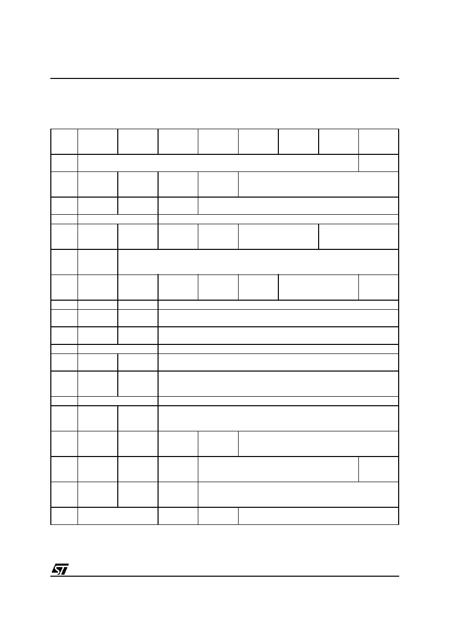
STV223XD/224XC - I≤C BUS SELECTION
41/76
6 I≤C BUS SELECTION
6.1 STV2238D: SUMMARY INPUT SIGNALS (WRITE MODE)
"Not-to-be-used" data must be set to "0".
Reg.
Addr.
(Hex)
DATA D7
DATA D6
DATA D5
DATA D4
DATA D3
DATA D2
DATA D1
DATA D0
00
PIFVCO Free Running Fine Adjustment
Not to
be used
01
PIF
Over-modu-
lation
AFC
Defeat
L/L' Mode
NEG/POS
Modulation
PIFVCO Free Running Coarse Adjustment
02
CVBS Out-
put
Overmodu-
lation Reset
Not to be
used bit
INTCVBS Output Amplitude Adjustment
03
Tuner AGC gain
Tuner AGC Starting Point Adjustment
04
Intercarrier
Filter ON/
OFF
QSS and AM
demod
defeat
FM/AM
Output
Selection
FM Demod.
Defeat
FM deviation and FM
De-emphasis
Main Audio Output
selection (int./ext.)
05
Volume
Control
Curve
Volume Control
06
Not to be
used
QSS/
Inter-carrier
CVBS Mute
SAW Filter
Switch
AGC SIF
Time Con-
stant
Sound
Standard Selection
PIF VCO
compensa-
tion
07
Blue Screen CO Insertion
Contrast
08
Oversize
Blanking
Half
Contrast
Saturation
09
CO Blanking
RGB
Blanking
Brightness
0A
RGBext/YCrCb Insertion
Red Drive Adjustment
0B
NTSC Set-
up
Black
Stretch
Green Drive Adjustment
0C
LSB RED
Cut-off
Counter
CO Freeze
Blue Drive Adjustment
0D
Manual Cut-off Selection
Red Cut-off Adjustment
0E
LSB GREEN
Cut-off
Counter
Not to be
used
Green Cut-off Adjustment
0F
White inser-
tion ON/OFF
CVBS2
ON/OFF
Chroma
Trap ON/
OFF
Coring
ON/OFF
Peaking
10
Not to be
used
CRT/LCD
Display
RGBosd
Contrast
Selection
APR Threshold
APR on/off
11
ACCO
ON/OFF
NTSC 104
Matrix
PAL/NTSC
Demod.
Gain
Bell Filter Shift
12
Not to be used
Chroma DL
ON/OFF
Chroma Out
ON/OFF
Bandpass Shift
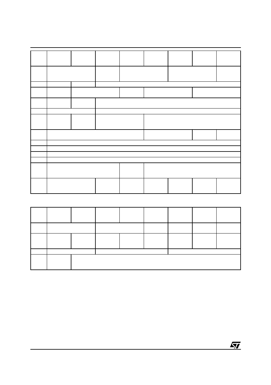
STV223XD/224XC - I≤C BUS SELECTION
42/76
6.2 STV2238D: SUMMARY OUTPUT SIGNALS (READ MODE)
13
Not to be used
Crystal In-
put Pin Disa-
ble
Chroma Standard Selec-
tion
Crystal Selection
3rd Crystal
14
Flesh Char. Flesh on/off
HUE
15
Safety Reset
Not to be used
SVHS switch
Second Video Switch Con-
trol
Main Video
Switch Control
16
Interlace
HOUT Disa-
ble
Horizontal Shift
17
50/60Hz Selection
Vertical Amplitude
18
Vertical
Sync ON/
OFF
Line Sync
ON/OFF
PLL1 Time Constant
Vertical Position
19
Not to be used
Noise Detector
Threshold
Long Blank-
ing
4/3-16/9
1A
Manual Cut-off Register - Red
1B
Manual Cut-off Register - Green
1C
Manual Cut-off Register - Blue
1D
Not to be used or CVBS1out (SDIP56, pin 29)
1E
Not to be used
AGC SIF
time con-
stant
Not to be used
1F
Audio Out
(Mono or Sound subcarri-
ers)
AVL
On/Off
AVL Time
Constant
Luma Delay
Shift
Not to be
used
Sound Sta-
tus Refresh
VOUT
Inhibition
Reg.Ad
dr.
(Hex)
DATA D7
DATA D6
DATA D5
DATA D4
DATA D3
DATA D2
DATA D1
DATA D0
00
Chroma Standard
Selection Status
Crystal Selection Status
Video Ident.
Status
Field Lock
Status
50/60 Hz
Status
Power ON
Reset
01
FM Dem.
VCO Cal.
Status
Scanning
VCO Cal.
Status
FBosd
Detection
FBext De-
tection
Safety
Status
Horizontal
Lock Status
Noise Detec-
tor Status
SVHS
Status
02
Cut-off loop status
FM Sound Carrier Levels
Digital AF Status
03
Tuner AGC
Output Sta-
tus
IC Identification
Reg.
Addr.
(Hex)
DATA D7
DATA D6
DATA D5
DATA D4
DATA D3
DATA D2
DATA D1
DATA D0
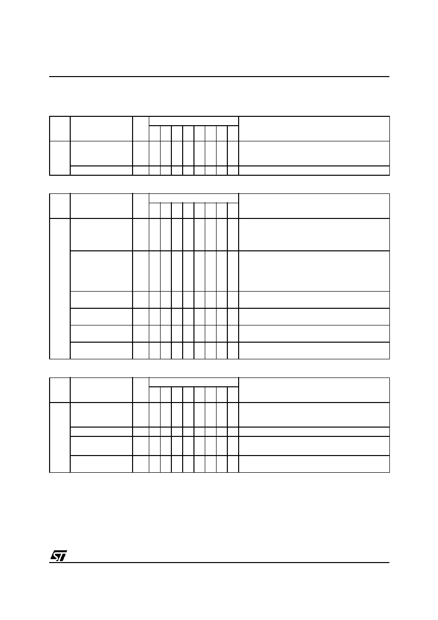
STV223XD/224XC - I≤C BUS SELECTION
43/76
6.3 STV2238D: INPUT SIGNALS (WRITE MODE)
Not used data bits must be set to "0".
PIFVCO FREE RUNNING FINE
PIF FREE RUNNING COARSE
PIF FEATURES
Reg.
Addr.
(Hex)
Description
Bits
Data
Comments
d7 d6 d5 d4 d3 d2 d1 d0
00
PIFVCO
Free Running
Fine Adjustment
7
0
1
1
0
0
1
0
0
1
0
0
1
0
0
1
0
0
1
0
0
1
X
X
X
PIF Typical + 0.7 MHz.
PIF Free Running mid range.
PIF Typical - 0.7 MHz.
Not to be used
1
X
X
X
X
X
X
X
0
Reg.
Addr.
(Hex)
Description
Bits
Data
Comments
d7 d6 d5 d4 d3 d2 d1 d0
01
PIFVCO Free
Running Coarse
Adjustment for
38.9 MHz Carrier
4
X
X
X
X
X
X
0
0
0
X
X
X
0
0
1
0
1
1
0
1
1
0
1
1
PIFVCO = F0 + 2.0 MHz.
PIFVCO = F0 (mid range).
PIFVCO = F0 - 1.8 MHz.
PIFVCO Free
Running Coarse
Adjustment for
33.9 MHz Carrier
(L')
4
X
X
X
X
X
X
1
1
1
1
1
1
0
0
1
0
1
1
0
1
1
0
1
1
PIFVCO = F0 + 1.3 MHz.
PIFVCO = F0 (mid range).
PIFVCO = F0 - 1.2 MHz.
PIF Modulation
1
X
X
X
X
X
X
0
1
X
X
X
X
X
X
X
X
0 = Negative Modulation.
1 = Positive Modulation.
L/L' Standard
Selection
1
X
X
X
X
0
1
1
1
X
X
X
X
X
X
X
X
0 = L Standard.
1 = L' Standard.
Digital AFC Defeat
1
X
X
0
1
X
X
X
X
X
X
X
X
X
X
X
X
0 = AFC Active.
1 = AFC Defeat (read register 02, d2 d1 d0 = 000).
PIF
Over-modulation
1
0
1
X
X
X
X
X
X
X
X
X
X
X
X
X
X
0 = Over-modulation detection off.
1 = Over-modulation regulation active.
Reg.
Addr.
(Hex)
Description
Bits
Data
Comments
d7 d6 d5 d4 d3 d2 d1 d0
02
CVBS Output Ampli-
tude
5
X
X
X
X
X
X
X
X
X
0
1
1
0
0
1
0
0
1
0
0
1
0
0
1
V
Typ.
- 1.6 dB.
V
Typ.
= 1.6 V (black / white).
V
Typ.
+ 1.5 dB.
Not to be used
1
X
X
0
X
X
X
X
X
Overmodulation
Reset
1
X
X
0
1
X
X
X
X
X
X
X
X
X
X
X
X
0 = Normal Operating Mode
1 = Overmodulation Reset
CVBS Output
1
0
1
X
X
X
X
X
X
X
X
X
X
X
X
X
X
0 = 2
VPP
, no external sound trap.
1 = 2.3
VPP
, external sound trap.
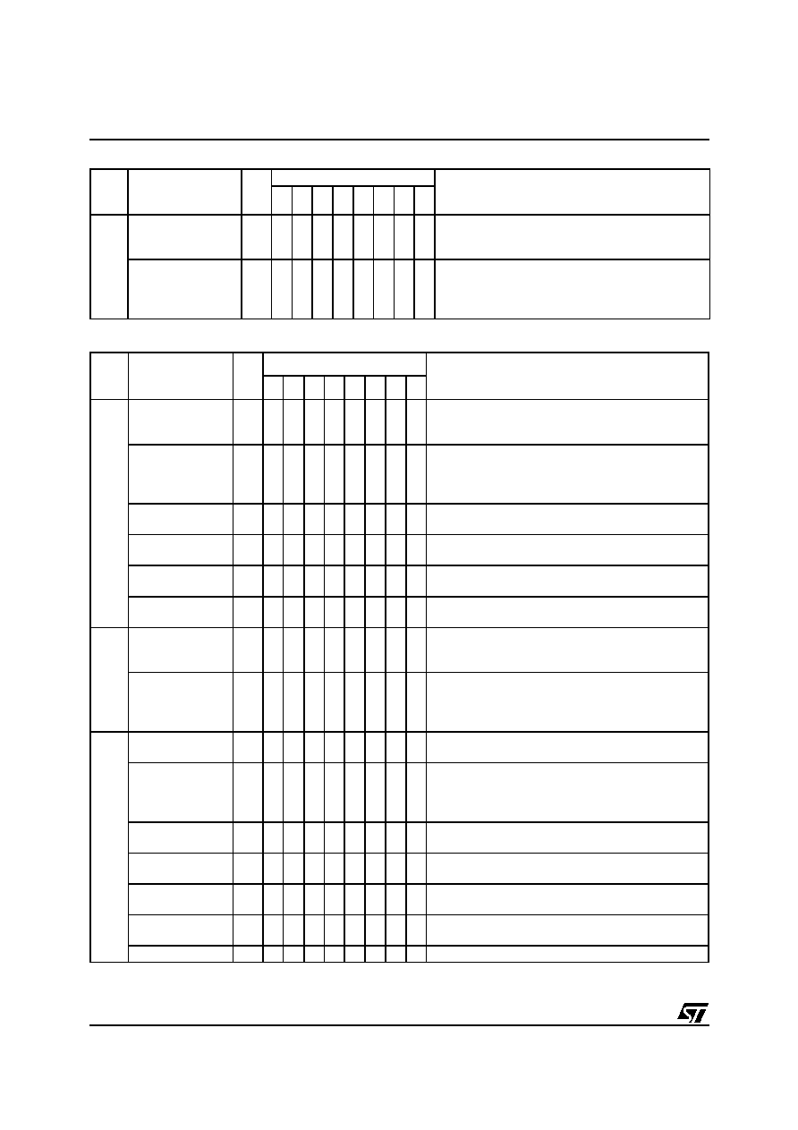
STV223XD/224XC - I≤C BUS SELECTION
44/76
TUNER DELAY
SIF FEATURES AND AUDIO SWITCHES
Reg.
Addr.
(Hex)
Description
Bits
Data
Comments
d7 d6 d5 d4 d3 d2 d1 d0
03
Tuner AGC Starting
Point Adjustment
6
X
X
X
X
X
X
0
1
1
0
0
1
0
0
1
0
0
1
0
0
1
0
0
1
Min. Start point 2 mV
RMS
at PIF input.
Typ. Start point 12 mV
RMS
at PIF input.
Max. Start point 80 mV
RMS
at PIF input
Tuner AGC Gain
2
0
0
1
1
0
1
0
1
X
X
X
X
X
X
X
X
X
X
X
X
X
X
X
X
X
X
X
X
X
X
X
X
50 µA/dB.
95 µA/dB.
170 µA/dB.
270 µA/dB.
Reg.
Addr
(Hex)
Description
Bits
Data
Comments
d7 d6 d5 d4 d3 d2 d1 d0
04
Main Audio Output
2
X
X
X
X
X
X
X
X
X
X
X
X
X
X
X
X
X
X
0
0
1
0
1
X
FM/AM audio selected.
External audio selected.
MUTE selected.
FM De-emphasis
Switch and FM de-
viation range con-
trol
2
X
X
X
X
X
X
X
X
X
X
X
X
X
X
X
X
0
0
1
1
0
1
0
1
X
X
X
X
X
X
X
X
Automatic control, according to sound standard.
Deemphasis at 75 µs and FM deviation at
±
25 kHz.
Deemphasis at 50 µs and FM deviation at
±
50 kHz.
Deemphasis filter bypassed.
FM demodulator
defeat
1
X
X
X
X
X
X
0
1
X
X
X
X
X
X
X
X
0 = FM demodulator active.
1 = FM demodulator defeat, FM out muted.
AM/FM output se-
lection
1
X
X
X
X
0
1
X
X
X
X
X
X
X
X
X
X
0 = FM output selected.
1 = AM output selected.
QSS and AM de-
modulator defeat
1
X
X
0
1
X
X
X
X
X
X
X
X
X
X
X
X
0 = QSS and AM demod active,
1 = QSS and AM demod not active (OFF)
Intercarrier filter
ON/OFF
1
0
1
X
X
X
X
X
X
X
X
X
X
X
X
X
X
0 = Intercarrier filter ON
1 = Intercarrier filter OFF
05
Volume Control
Attenuation,
Linear curve (dB)
1
0
0
0
1
0
1
0
1
0
1
0
1
0
1
0
1
Attenuation = 0 dB.
Attenuation = 78 dB.
7-bit resolution.
Volume Control
Attenuation,
Non-linear curve
(d0 = 0, d7 = 1)
1
1
1
0
1
0
1
0
1
0
1
0
1
0
1
0
0
Attenuation = 0 dB.
Attenuation = 78 dB.
6-bit resolution.
06
PIF VCO compen-
sation
1
X
X
X
X
X
X
X
X
X
X
X
X
X
X
0
1
0 = Optimized for PIF from 33.9 to 38.9 MHz
1 = Optimized for PIF 45.75 & 58.75 MHz
Sound standard
selection
2
X
X
X
X
X
X
X
X
X
X
X
X
X
X
X
X
X
X
X
X
0
0
1
1
0
1
0
1
X
X
X
X
6.5 MHz sound selected.
6.0 MHz sound selected.
5.5 MHz sound selected.
4.5 MHz sound selected.
AGC SIF time
constant (AM)
1
X
X
X
X
X
X
X
X
0
1
X
X
X
X
X
X
0 = auto time constant.
1 = fast time constant forced.
SAW filter switch
output
1
X
X
X
X
X
X
0
1
X
X
X
X
X
X
X
X
0 = output low (0.4 V Max.).
1 = output high (4 V Min.).
CVBS output
(from PIF circuit)
1
X
X
X
X
0
1
X
X
X
X
X
X
X
X
X
X
0 = CVBS output enable.
1 = CVBS output muted.
QSS/Inter-carrier
Application
1
X
X
0
1
X
X
X
X
X
X
X
X
X
X
X
X
0 = QSS application, intercarrier filter OFF
1 = Intercarrier application.
Not to be used
1
0
X
X
X
X
X
X
X
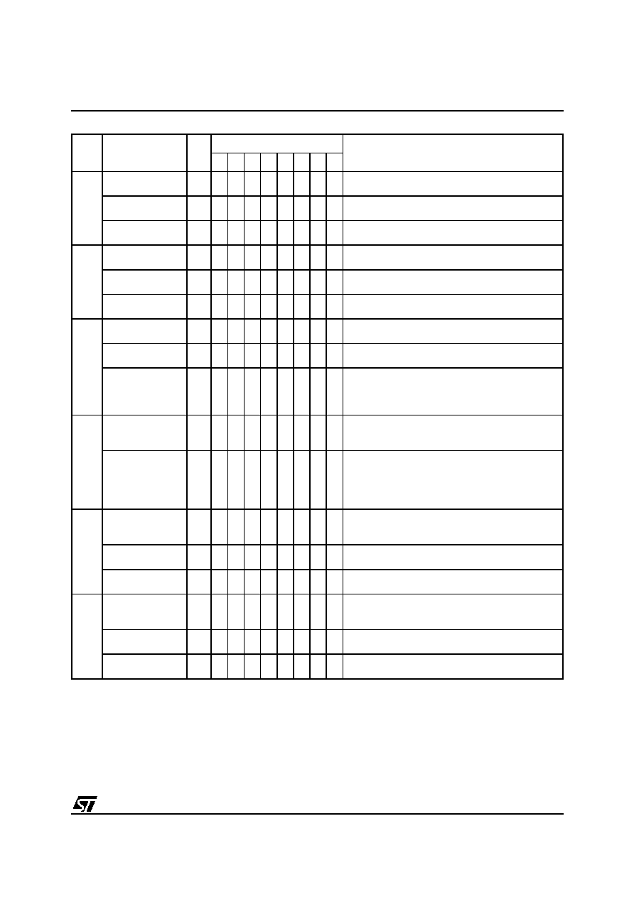
STV223XD/224XC - I≤C BUS SELECTION
45/76
VIDEO CONTROLS
Reg.
Addr
(Hex)
Description
Bits
Data
Comments
d7 d6 d5 d4 d3 d2 d1 d0
07
Contrast control
6
X
X
X
X
0
1
0
1
0
1
0
1
0
1
0
1
-24 dB gain (Min. contrast).
0 dB gain (Max. contrast).
Cut-off pulse inser-
tion
1
X
X
0
1
X
X
X
X
X
X
X
X
X
X
X
X
0 = After internal frame blanking.
1 = After Vertical oversize blanking (a08d7 = 1).
Blue screen fea-
ture
1
0
1
X
X
X
X
X
X
X
X
X
X
X
X
X
X
0 = Blue screen OFF.
1 = Blue screen ON.
08
Saturation control
6
X
X
X
X
0
1
0
1
0
1
0
1
0
1
0
1
-40 dB gain (Min. saturation).
+9 dB gain (Max. saturation).
Half contrast ena-
ble
1
X
X
0
1
X
X
X
X
X
X
X
X
X
X
X
X
0 = Disabled.
1 = Enabled.
Oversize blanking
enable
1
0
1
X
X
X
X
X
X
X
X
X
X
X
X
X
X
0 = Disabled.
1 = Enabled.
09
Brightness control
6
X
X
X
X
0
1
0
1
0
1
0
1
0
1
0
1
-30% of B/W at Max. contrast.
+30% of B/W at Max. contrast.
RGB blanking
1
X
X
0
1
X
X
X
X
X
X
X
X
X
X
X
X
0 = Not active (normal operation).
1 = Active.
Cut-off blanking
1
0
1
X
X
X
X
X
X
X
X
X
X
X
X
X
X
0 = Enable: RGB output blanked when I
CATH
voltage
is far from internal cut-off reference (cut-off loop not
locked), during IC start-up.
1 = Disable: RGB output not blanked by cut-off loop.
0A
Red drive adjust-
ment (white point
R)
6
X
X
X
X
0
1
0
1
0
1
0
1
0
1
0
1
-6 dB gain (Min. drive).
0 dB gain (Max. drive).
RGBext/YCrCb
Selection
2
0
0
1
1
0
1
0
1
X
X
X
X
X
X
X
X
X
X
X
X
X
X
X
X
X
X
X
X
X
X
X
X
RGB ext. insertion enable, controlled by FBext input
pin.
RGB ext. insertion disable, FBext control disable.
RGB ext. insertion forced (FBext not active).
YCrCb insertion forced.
0B
Green drive adjust-
ment
(white point G)
6
X
X
X
X
0
1
0
1
0
1
0
1
0
1
0
1
-6 dB gain (Min. drive).
0 dB gain (Max. drive).
Black stretch ena-
ble
1
X
X
0
1
X
X
X
X
X
X
X
X
X
X
X
X
0 = Black stretch disable.
1 = Black stretch enable.
Black Stretch
Reference Level
1
0
1
X
X
X
X
X
X
X
X
X
X
X
X
X
X
0 = 0 IRE (no set-up).
1 = 7.5 IRE (NTSC set-up).
0C
Blue drive adjust-
ment
(white point B)
6
X
X
X
X
0
1
0
1
0
1
0
1
0
1
0
1
-6 dB gain (Min. drive).
0 dB gain (Max. drive).
Cut-off loop control
1
X
X
0
1
X
X
X
X
X
X
X
X
X
X
X
X
0 = Cut-off loop active.
1 = Cut-off loop frozen.
LSB (9th bit) Red
cut-off counter
1
0
1
X
X
X
X
X
X
X
X
X
X
X
X
X
X
Red LSB = 0
Red LSB = 1
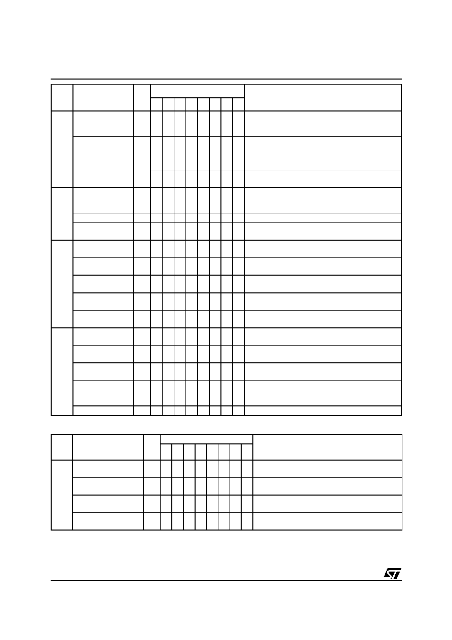
STV223XD/224XC - I≤C BUS SELECTION
46/76
CHROMA CONTROLS
0D
Red cut-off adjust-
ment (Black point
R)
6
X
X
X
X
0
1
0
1
0
1
0
1
0
1
0
1
-150 mV.
+150 mV.
Manual Cut-off Se-
lection
2
0
1
0
1
X
X
X
X
X
X
X
X
X
X
X
X
Automatic Cut-off application, data = 00hex in
registers 1A,1B, 1C.
Manual cut-off application DC at R,G,B output are
adjusted thanks registers 1A, 1B, 1C.
0
1
1
0
X
X
X
X
X
X
X
X
X
X
X
X
Not allowed.
Not allowed.
0E
Green cut-off ad-
justment (Black
point G)
6
X
X
X
X
0
1
0
1
0
1
0
1
0
1
0
1
-150 mV.
+150 mV.
Not to be used
1
X
0
X
X
X
X
X
X
LSB (9th bit) Green
cut-off counter
1
0
1
X
X
X
X
X
X
X
X
X
X
X
X
X
X
Green LSB = 0
Green LSB = 1
0F
Peaking control
4
X
X
X
X
X
X
X
X
0
1
0
1
0
1
0
1
0 dB at center Freq. Min. peaking.
+ 6dB at center Freq.Max. peaking.
Coring on sharp-
ness
1
X
X
X
X
X
X
0
1
X
X
X
X
X
X
X
X
0 = Coring off.
1 = Coring on.
Chroma trap selec-
tion
1
X
X
X
X
0
1
X
X
X
X
X
X
X
X
X
X
0 = Trap on (CVBS mode & color identified).
1 = Trap off.
CVBS2 ON/OFF
1
X
X
0
1
X
X
X
X
X
X
X
X
X
X
X
X
0 = CVBS2 output active.
1 = CVBS2 output not active.
White insertion
1
0
1
X
X
X
X
X
X
X
X
X
X
X
X
X
X
0 = White insertion not active.
1 = White insertion enable during HOUT soft mode.
10
APR enable
1
X
X
X
X
X
X
X
X
X
X
X
X
X
X
0
1
0 = APR disable.
1 = APR enable.
APR threshold
5
X
X
X
X
X
X
0
1
0
1
0
1
0
1
X
X
50 IRE.
100 IRE.
RGB OSD contrast
selection
1
X
X
X
X
0
1
X
X
X
X
X
X
X
X
X
X
0 = Contrast control disable.
1 = Contrast control enable.
CRT/LCD Display
1
X
X
0
1
X
X
X
X
X
X
X
X
X
X
X
X
0 = RGB output blanking active, CRT Display
1 = RGB output blanking replaced by black level,
LCD Display
Not to be used
2
0
X
X
X
X
X
X
x
Reg.
Addr
(Hex)
Description
Bits
Data
Comments
d7 d6 d5 d4 d3 d2 d1 d0
Reg.
Addr.
(Hex)
Description
Bits
Data
Comments
d7 d6 d5 d4 d3 d2 d1 d0
11
Bell filter adjust
5
X
X
X
X
X
X
0
1
0
1
0
1
0
1
0
1
0 kHz.
+100 kHz.
PAL/NTSC
demodulation gain
1
X
X
X
X
0
1
X
X
X
X
X
X
X
X
X
X
0 = 0 dB gain (nominal).
1 = +6 dB gain.
NTSC matrix
1
X
X
0
1
X
X
X
X
X
X
X
X
X
X
X
X
0 = 90∞ matrix selection.
1 = 104∞ matrix selection (in NTSC only).
ACC overload disable
1
0
1
X
X
X
X
X
X
X
X
X
X
X
X
X
X
0 = ACC overload active.
1 = ACC overload disable.
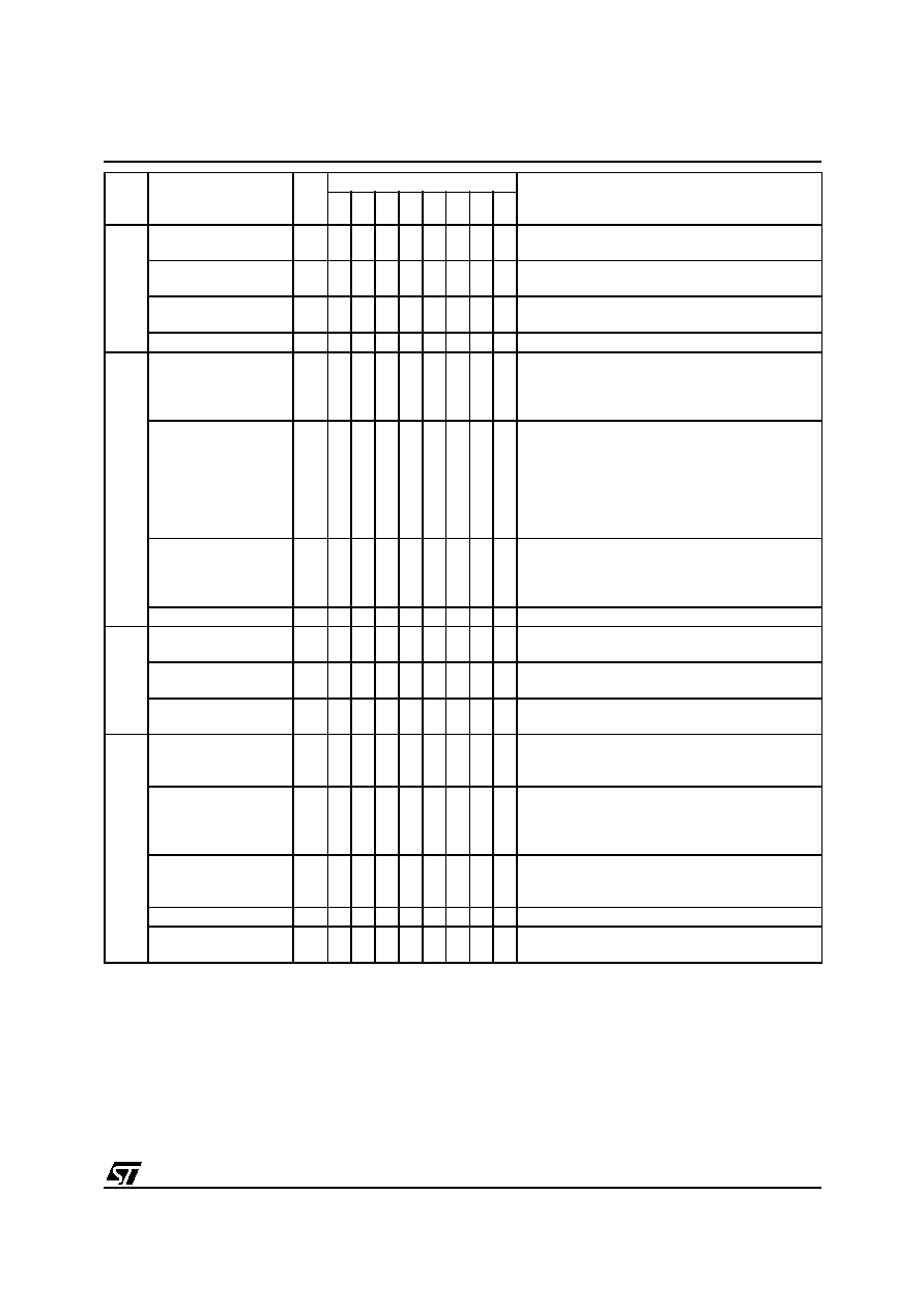
STV223XD/224XC - I≤C BUS SELECTION
47/76
12
Bandpass adjust
4
X
X
X
X
X
X
X
X
0
1
0
1
0
1
0
1
f = fosc.
f = 1.1*fosc.
Chroma reference out-
put
1
X
X
X
X
X
X
0
1
X
X
X
X
X
X
X
X
0 = Chroma reference output OFF.
1 = Chroma reference output ON.
Chroma DL selection
1
X
X
X
X
0
1
X
X
X
X
X
X
X
X
X
X
0 = ON.
1 = OFF.
Not to be used
2
0
0
X
X
X
X
X
X
13
Crystal selection
2
X
X
X
X
X
X
X
X
X
X
X
X
X
X
X
X
X
X
X
X
0
0
1
1
0
1
0
1
X
X
X
X
XTAL1 (4.43/3.5XX MHz).
XTAL2 (3.5XX MHz).
XTAL3 (3.5XX MHz).
Not allowed.
Standard selection
2
X
X
X
X
X
X
X
X
X
X
X
X
X
X
X
X
X
X
X
X
X
0
0
1
1
1
1
X
0
1
0
0
0
1
X
X
X
0
0
1
X
1
X
X
0
1
0
X
1
X
X
0
X
X
X
X
PAL.
NTSC.
SECAM (only with XTAL1).
Not allowed.
Not allowed.
AUTO mode.
Not allowed
Crystal inhibition
2
X
X
X
X
X
X
X
X
0
0
1
1
X
X
X
X
X
X
X
X
X
X
X
X
X
X
X
X
0
1
0
1
Two-crystal, P/S/N application.
Three-crystal, P/N application.
One-crystal, 4.43 MHz application.
Two-crystal, P/N application.
Not to be used
2
0
0
X
X
X
X
X
X
14
Hue control
(in NTSC only)
6
X
X
X
X
0
1
0
1
0
1
0
1
0
1
0
1
-45∞.
+45∞.
Flesh enable
1
X
X
0
1
X
X
X
X
X
X
X
X
X
X
X
X
0 = Flesh disable (OFF).
1 = Flesh enable (ON).
Wide flesh charac-
teristic selection
1
0
1
X
X
X
X
X
X
X
X
X
X
X
X
X
X
0 = Normal characteristic.
1 = Wide characteristic.
15
Main Video switch
2
X
X
X
X
X
X
X
X
X
X
X
X
X
X
X
X
X
X
0
0
1
0
1
X
CVBS1 selected.
CVBS2 selected.
Y/CVBS3 selected.
Second Video switch
control
2
X
X
X
X
X
X
X
X
X
X
X
X
X
X
X
X
0
0
1
1
0
1
0
1
X
X
X
X
X
X
X
X
CVBS1 selected.
CVBS2 selected.
Y/CVBS3 selected.
Y+C selected.
SVHS switch Chroma
decoder input
selection
1
X
X
X
X
X
X
0
1
X
X
X
X
X
X
X
X
0 = Main CVBS selected.
1 = CHR input selected (SVHS).
Not to be used
3
X
0
0
X
X
X
X
X
Safety Reset
1
0
1
X
X
X
X
X
X
X
X
X
X
X
X
X
X
0 = Safety active
1 = Reset Safety, Safety non-active
Reg.
Addr.
(Hex)
Description
Bits
Data
Comments
d7 d6 d5 d4 d3 d2 d1 d0
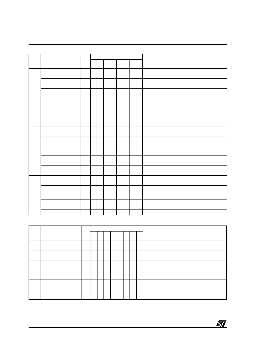
STV223XD/224XC - I≤C BUS SELECTION
48/76
SCANNING CONTROLS
MISCELLANEOUS
Reg.
Addr.
(Hex)
Description
Bits
Data
Comments
d7 d6 d5 d4 d3 d2 d1 d0
16
Horizontal shift
6
X
X
X
X
0
1
0
1
0
1
0
1
0
1
0
1
-2.5 µs.
+2.5 µs.
Horizontal output
pulse disable
1
X
X
0
1
X
X
X
X
X
X
X
X
X
X
X
X
0 = Normal mode.
1 = HOUT disable (high level).
Interlace
1
0
1
X
X
X
X
X
X
X
X
X
X
X
X
X
X
0 = Interlace mode.
1 = De-interlace mode.
17
Vertical amplitude
6
X
X
X
X
0
1
0
1
0
1
0
1
0
1
0
1
1.5 V on V
AMP
Pin.
6.0 V on V
AMP
Pin.
50/60Hz selection
2
0
0
1
1
0
1
0
1
X
X
X
X
X
X
X
X
X
X
X
X
X
X
X
X
X
X
X
X
X
X
X
X
Auto (50 Hz when no ident.).
60 Hz.
50 Hz.
Auto (60 Hz when no ident.).
18
Vertical position
4
X
X
X
X
X
X
X
X
0
1
0
1
0
1
0
1
4 V high level on VOUT Pin.
6 V high level on VOUT Pin.
PLL1 time constant
2
X
X
X
X
X
X
X
X
0
0
1
1
0
1
0
1
X
X
X
X
X
X
X
X
X
X
X
X
X
X
X
X
Auto time constant selection.
Short time constant.
Long time constant.
Very long time constant.
Horizontal synchroni-
zation
1
X
X
0
1
X
X
X
X
X
X
X
X
X
X
X
X
0 = PLL1 active.
1 = PLL1 not active (horiz. free running mode).
Vertical synchroniza-
tion
1
0
1
X
X
X
X
X
X
X
X
X
X
X
X
X
X
0 = Vertical synchronization active.
1 = Vertical free running mode.
19
4/3 16/9 selection
1
X
X
X
X
X
X
X
X
X
X
X
X
X
X
0
1
0 = 0.1 V low level on VOUT Pin.
1 = 2 V low level on VOUT Pin.
Frame blanking
1
X
X
X
X
X
X
X
X
X
X
X
X
0
1
X
X
0 = Adapted to standard.
1 = Long blanking (50 Hz blanking) both in 50 Hz
and 60 Hz modes
Noise detector thresh-
old
2
X
X
X
X
X
X
X
X
0
1
0
1
X
X
X
X
Low threshold.
High threshold.
Not to be used
4
0
0
0
0
X
X
X
X
Reg.
Addr.
(Hex)
Description
Bits
Data
Comments
d7 d6 d5 d4 d3 d2 d1 d0
1A
Manual Cut-off
Register Red
8
0
1
0
1
0
1
0
1
0
1
0
1
0
1
0
1
Low DC at RGB output.
High DC at RGB output.
1B
Manual Cut-off
Register Green
8
0
1
0
1
0
1
0
1
0
1
0
1
0
1
0
1
Low DC at RGB output.
High DC at RGB output.
1C
Manual Cut-off
Register Blue
8
0
1
0
1
0
1
0
1
0
1
0
1
0
1
0
1
Low DC at RGB output.
High DC at RGB output.
1D
CVBS1 Out selection
at pin 29 SDIP56
8
0
0
0
0
0
0
0
0
0
0
1
0
1
0
1
0
CVBS1 Out selected at pin 29 SDIP56.
TQFP64 packages must be set to 0h.
1E
Not To Be Used
7
0
0
0
X
0
0
0
0
SIF AGC time
constant (positive
modulation)
1
0
0
0
0
0
0
0
1
0
0
0
0
0
0
0
0
Automatic SIFAGC Time constant control.
Forced Long time constant.
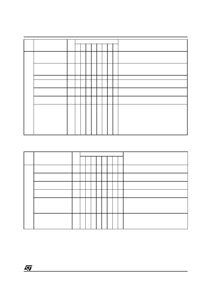
STV223XD/224XC - I≤C BUS SELECTION
49/76
6.4 OUTPUT SIGNALS (READ MODE)
OUTPUT SIGNALS (READ MODE)
1F
VOUT Inhibition
1
X
X
X
X
X
X
X
X
X
X
0
0
X
X
0
1
VOUT normal operating.
VOUT inhibition (forced to high DC level control-
led by vertical position register).
Sound Level Status
Refresh
1
X
X
X
X
X
X
X
X
X
X
0
0
0
1
X
X
0 = Sound level status continuously refreshed
1 = Sound level status refreshed only at the end
of vertical synchronization pulse
Not to be used
1
X
X
X
X
X
0
X
X
Luma Delay Shift
1
X
X
X
X
X
X
X
X
0
1
0
0
X
X
X
X
Standard luma delay.
140 ns on luma delay.
AVL Time Constant
1
X
X
X
X
X
X
0
1
X
X
0
0
X
X
X
X
0 = Slow Timer Constant
1 = Fast Time Constant
AVL On/Off
1
X
X
X
X
0
1
X
X
X
X
0
0
X
X
X
X
0 = AVL Off
1 = AVL On
AM/FMOUT pin selec-
tion
2
0
0
1
1
0
1
0
1
X
X
X
X
X
X
X
X
X
X
X
X
0
0
0
0
X
X
X
X
X
X
X
X
Output of AM/FM demodulator.
Sound subcarriers selected.
Audio output muted.
Main audio switch output, either internal or exter-
nal audio depending on main audio switch selec-
tion.
reg04hex; d0 = 0: internal audio.
reg04hex; d0 = 1: external audio.
Reg.
Addr.
(Hex)
Description
Bits
Data
Comments
d7 d6 d5 d4 d3 d2 d1 d0
Reg.
Addr.
(Hex)
Description
Bits
Data
Comments
d7 d6 d5 d4 d3 d2 d1 d0
00
Power-on reset
1
X
X
X
X
X
X
X
X
X
X
X
X
X
X
0
1
Normal mode.
Power down mode.
Field frequency
1
X
X
X
X
X
X
X
X
X
X
X
X
0
1
X
X
50 Hz.
60 Hz.
Field lock status
1
X
X
X
X
X
X
X
X
X
X
0
1
X
X
X
X
Not locked.
Locked.
Video identification
1
X
X
X
X
X
X
X
X
0
1
X
X
X
X
X
X
No identification.
Video identification.
Standard status crystal se-
lection
2
X
X
X
X
X
X
X
X
0
0
1
1
0
1
0
1
X
X
X
X
X
X
X
X
X
X
X
X
X
X
X
X
XTAL1 (4.43 MHz).
XTAL2 (3.5X MHz).
XTAL3 (3.5X MHz).
XTAL1 (3.5X MHz).
Standard selection
2
0
0
1
1
0
1
0
1
X
X
X
X
X
X
X
X
X
X
X
X
X
X
X
X
X
X
X
X
X
X
X
X
PAL.
NTSC.
SECAM.
COLOR OFF.
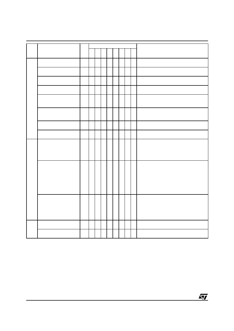
STV223XD/224XC - I≤C BUS SELECTION
50/76
01
SVHS status
1
X
X
X
X
X
X
X
X
X
X
X
X
X
X
0
1
No SVHS (CVBS mode).
SVHS mode.
Noise detection
1
X
X
X
X
X
X
X
X
X
X
X
X
0
1
X
X
High S/N.
Low S/N.
Scanning Horizontal
phase-locked loop status
1
X
X
X
X
X
X
X
X
X
X
0
1
X
X
X
X
Not locked.
Locked.
Safety status
1
X
X
X
X
X
X
X
X
0
1
X
X
X
X
X
X
Safety not active.
Safety active.
Fast Blanking detection on
external fast blanking pin
(during frame retrace)
1
X
X
X
X
X
X
0
1
X
X
X
X
X
X
X
X
No insertion detected.
Insertion on FBext.
Fast blanking detection on
OSD fast blanking pin
(during frame retrace)
1
X
X
X
X
0
1
X
X
X
X
X
X
X
X
X
X
No insertion detected.
Insertion on FBosd.
Scanning VCO
calibration
1
X
X
0
1
X
X
X
X
X
X
X
X
X
X
X
X
Not calibrated.
Calibrated.
FM demodulation VCO
calibration
1
0
1
X
X
X
X
X
X
X
X
X
X
X
X
X
X
Not calibrated.
Calibrated.
02
Digital AFC status
3
X
X
X
X
X
X
X
X
X
X
X
X
X
X
X
X
X
X
X
X
X
X
X
X
X
0
0
0
1
1
1
1
0
0
0
1
0
0
0
1
F
PLL
- F0 < -300 kHz.
-300 kHz < F
PLL
- F0 < -60 kHz.
-60 kHz < F
PLL
- F0 < +60 kHz.
+60 kHz < F
PLL
- F0 < +300 kHz.
+300 kHz < F
PLL
- F0.
Sound carrier level
3
X
X
X
X
X
X
X
X
X
X
X
X
X
X
X
X
0
0
0
0
1
1
1
1
0
0
1
1
1
1
0
0
0
1
1
0
0
1
1
0
X
X
X
X
X
X
X
X
X
X
X
X
X
X
X
X
X
X
X
X
X
X
X
X
Level 1 (low sound carrier signal).
Level 2.
Level 3.
Level 4.
Level 5.
Level 6.
Level 7.
Level 8 (high sound carrier signal)
Blue cut-off register and
cut-off loop status
2
0
0
1
1
0
1
0
1
X
X
X
X
X
X
X
X
X
X
X
X
X
X
X
X
X
X
X
X
X
X
X
X
Blue CO register <011110000
Blue CO register >100001111
011110000< Blue Co register <100001111
and Icath not locked
011110000< Blue Co register <100001111
and Icath locked
03
IC identification
1
X
X
X
X
X
X
X
X
X
X
X
X
X
X
0
1
TQFP64
SDIP56
Tuner AGC Output Status
1
0
1
X
X
X
X
X
X
X
X
X
X
X
X
X
X
Tuner AGC Output not active
Tuner AGC Output active
Reg.
Addr.
(Hex)
Description
Bits
Data
Comments
d7 d6 d5 d4 d3 d2 d1 d0
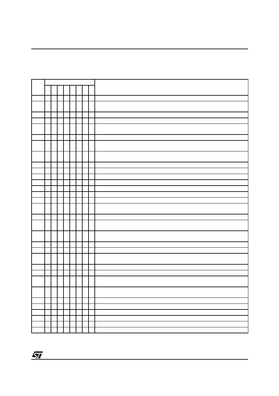
STV223XD/224XC - I≤C BUS SELECTION
51/76
6.5 POWER-ON RESET - INITIAL BUS REGISTER CONDITIONS
Power-On Reset is active when the power supply V
CCD
is below 3 Volts.
All data from all registers must be written by microprocessor after power-on. Unused data must be set to
0. POR values are not tested during production.
Reg.
Addr.
(Hex)
Initial Data Value
Comments
d7 d6 d5 d4 d3 d2 d1 d0
00
1
0
0
0
0
0
0
0
PIFVCO free running fine adjustment Typical.
01
0
0
0
0
0
1
1
1
PIFVCO coarse typ, BG = 38.9 MHz, Negative modulation, AFC active,
no PIF over-modulation regulation.
02
0
0
0
1
0
0
0
0
CVBS amplitude Typical, 2V
PP.
03
0
0
1
0
0
0
0
0
Tuner AGC starting point Typical, Tuner AGC gain Min.
04
0
0
0
0
0
0
0
0
FM/AM out selected, FM de-emphasis and FM deviation auto-control, FM demod.
active, FM out selected, QSS and AM demod. active.
05
0
1
1
1
1
1
1
1
Volume control attenuation at maximum, linear curve (dB).
06
0
0
0
0
0
0
0
0
PIF < 42 MHz, 6.5 MHz sound carrier selected, auto AGC SIF time constant, saw
filter switch control at low level, CVBS out enabled, QSS mode.
07
0
0
1
0
0
0
0
0
Contrast at middle, cut-off pulse insertion after internal frame blanking, blue screen
disabled.
08
0
0
1
0
0
0
0
0
Saturation at middle, half contrast disabled, oversize blanking disabled.
09
0
0
1
0
0
0
0
0
Brightness at middle, RGB Blanking not active.
0A
0
0
1
0
0
0
0
0
Red drive at middle, RGBext insertion enabled (FBext Pin control).
0B
0
0
1
0
0
0
0
0
Green drive at middle, black stretch disabled, black stretch ref 0IRE.
0C
0
0
1
0
0
0
0
0
Blue drive at middle, cut-off loop active.
0D
0
0
1
0
0
0
0
0
Red cut-off at middle, automatic cut-off loop.
0E
0
0
1
0
0
0
0
0
Green cut-off at middle.
0F
0
0
0
0
1
0
0
0
Peaking on luma at middle, coring off, trap ON(CVBS & color identified), CVBS2 ON,
white insertion not active.
10
0
0
0
1
0
0
0
0
APR disabled, APR threshold at middle, RGB OSD contrast disabled.
11
0
0
0
0
0
0
0
0
No shift of bell filter center frequency, 0dB P/N demod. gain, 90∞ matrix selection,
ACC overload ON.
12
0
0
0
0
0
0
0
0
No shift of bandpass center frequency, chroma reference output off, chroma delay
line on.
13
0
0
0
0
0
0
0
0
Two crystals application P/S/N, PAL XTAL1 forced mode, two crystal applications.
14
0
0
1
0
0
0
0
0
Hue at middle, flesh disabled, normal flesh characteristic.
15
0
0
0
0
0
0
0
0
CVBS1 selected on main CVBS output, CVBS1 selected on second CVBS output,
CVBS mode.
16
0
0
1
0
0
0
0
0
Horizontal shift at middle, horizontal output enabled, interlace mode.
17
0
0
1
0
0
0
0
0
Vertical amplitude at middle, auto 50/60 Hz identification.
18
0
0
0
0
1
0
0
0
Vertical position at middle, automatic time constant selection on PLL1, PLL1 active,
Vertical synchronization active.
19
0
0
0
0
0
0
0
0
0.1 V low level at pin VOUT, frame blanking adapted to standard, noise detector low
threshold.
1A
0
0
0
0
0
0
0
0
Not active, auto cut-off.
1B
0
0
0
0
0
0
0
0
Not active, auto cut-off.
1C
0
0
0
0
0
0
0
0
Not active, auto cut-off.
1D
0
0
0
0
0
0
0
0
R-Y output at pin 29 (SDIP56) or at pin 41 (TQFP64)
1E
0
0
0
0
0
0
0
0
Not to be used, except d4: Auto. SIF AGC time constant control in L/L' standards.
1F
0
0
0
0
0
0
0
0
VOUT pulse active, standard luma delay, AVL off, AM/FM mono sound selected.
STV223XD/224XC - I≤C BUS SPECIFICATION COMPATIBILITY
52/76
7 I≤C BUS SPECIFICATION COMPATIBILITY
The STV2236D, 2237D, 2238D, 2239D/
STV2246C, 2286C, 2247C, 2248C and 2249C I≤C
bus specification is compatible between IC ver-
sion. However, some dedicated settings must be
used for the different versions. The following sec-
tions show the differences between the various
versions. An "X" means that the function is availa-
ble and can be set to "1" or "0".
TQFP64
SDIP56
2238D
2239D
2237D
2236D
2248C
2249C
2247C
2246C
2286C
SAW Filter switch
WR06d4
X
X
X
X
0
0
0
0
0
CVBSout2 on/off
WR0Fd6
X
X
X
X
0
0
0
0
0
RGBext
WR0A d7,d6
X
X
X
X
X
X
X
X
01
L/L' mode
WR01d5
X
0
0
0
X
0
0
0
0
Positive/negative modulation
WR01 d4
X
0
0
0
X
0
0
0
0
FM/AM output selection
WR04d5
X
0
0
0
X
0
0
0
0
Bell Filter
WR11 d4-d0
X
X
00000
00000
X
X
00000
00000
00000
QSS/Intercarrier application
WR06d6
X
X
X
1
X
X
X
1
1
QSS and AM defeat
WR04 d6
X
X
X
1
X
X
X
1
1
AGC SIF time constant
WR06 d3&WR1E d4
X
X
X
00
X
X
X
X
00
CVBSout amplitude
WR02 d4-d0
X
X
X
10000
X
X
X
X
10000
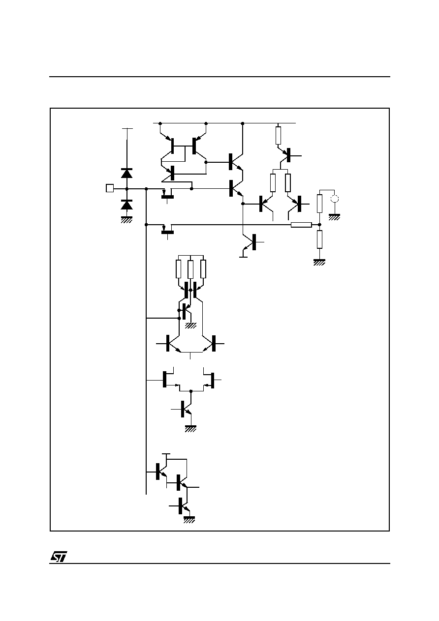
STV223XD/224XC - INPUT/OUTPUT SCHEMATIC DIAGRAMS
53/76
8 INPUT/OUTPUT SCHEMATIC DIAGRAMS
Figure 20. STV2238D (TQFP64)
1
SLPF
GND1
V
REF
V
CC1
V
CC1
V
CC1
(8 V)
V
CC1
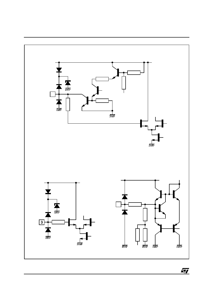
STV223XD/224XC - INPUT/OUTPUT SCHEMATIC DIAGRAMS
54/76
Figure 21. STV2238D (TQFP64)
V
CCD
(5V) (Pin 4 - TQFP64)
V
CCD
(5V) (Pin 4 - TQFP64)
V
CC2
(8V) (Pin 25 - TQFP64)
GND
IF
GND
IF
GND
IF
GND
IF
GNDD
GNDD
GNDD
SDA
5 V
10 k
AUDIOOUT
GNDD
GNDD
10 k
SCL
50
6
5 V
2
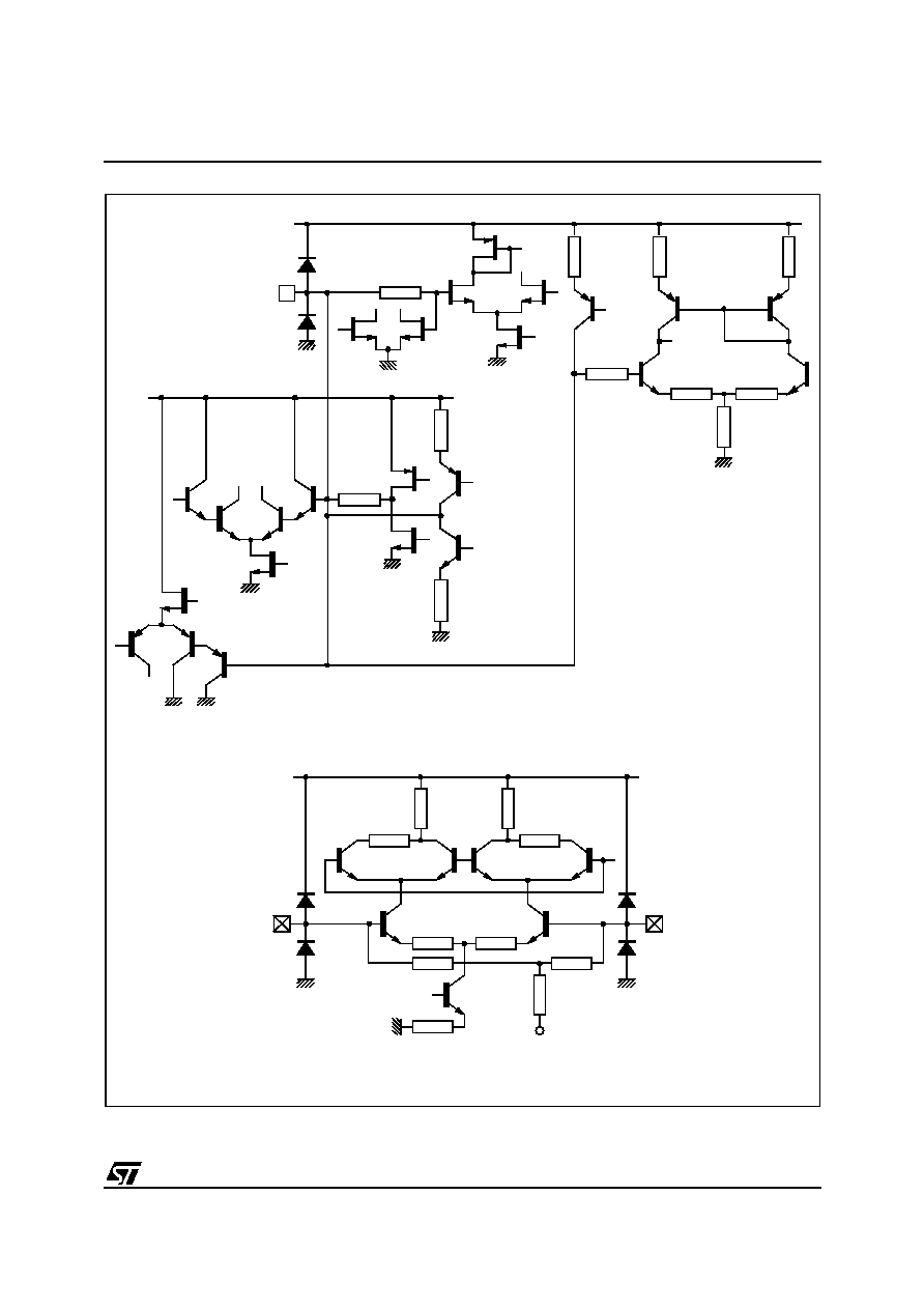
STV223XD/224XC - INPUT/OUTPUT SCHEMATIC DIAGRAMS
55/76
Figure 22. STV2238D (TQFP64) (continued)
FMCAP
V
CCIF
(5V) (Pin 20 - TQFP64)
V
CCIF
(5V) (Pin 20 - TQFP64)
SIFIN1, PIFIN1
Pins 8 - 13
SIFIN2, PIFIN2
Pins 9 - 14
GND
IF
GND
IF
GND
IF
GND
IF
GND
IF
GND
IF
GND
IF
GND
IF
GND
IF
GND
IF
GND
IF
V
CCIF
(5V) (Pin 20 - TQFP64)
2.5 V
7
50

STV223XD/224XC - INPUT/OUTPUT SCHEMATIC DIAGRAMS
56/76
Figure 23. STV2238D (TQFP64) (continued)
V
CCIF
(5V) (Pin 20 - TQFP64)
V
CCIF
(5V) (Pin 20 - TQFP64)
GND
IF
GND
IF
GND
IF
GND
IF
GND
IF
GND
IF
GND
IF
GND
IF
GND
IF
AGCSIFCAP 10
V
REF
IF
11
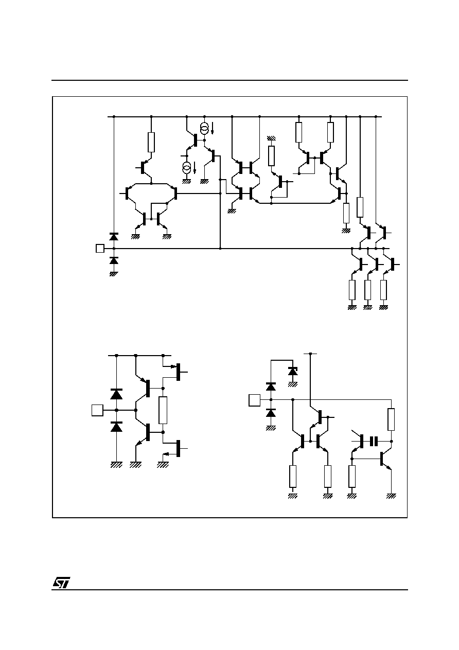
STV223XD/224XC - INPUT/OUTPUT SCHEMATIC DIAGRAMS
57/76
Figure 24. STV2238D (TQFP64) (continued)
V
CCIF
(5V) (Pin 20 - TQFP64)
V
CCIF
(5V) (Pin 20 - TQFP64)
V
CCIF
(5V) (Pin 20 - TQFP64)
GND
IF
GND
IF
GND
IF
GND
IF
GND
IF
GND
IF
GND
IF
GND
IF
GND
IF
GND
IF
GND
IF
GND
IF
GND
IF
GND
IF
GND
IF
TUNER-
AGCOUT
SAWSWI
AGCPIFCAP
12
12 V
16
15
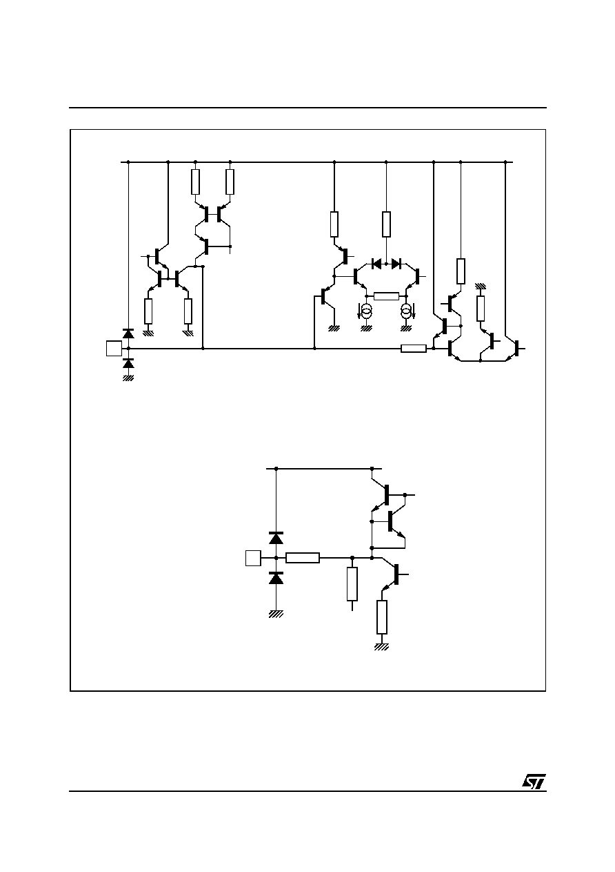
STV223XD/224XC - INPUT/OUTPUT SCHEMATIC DIAGRAMS
58/76
Figure 25. STV2238D (TQFP64) (continued)
V
CCIF
(5V) (Pin 20 - TQFP64)
V
CC2
(8V) (Pin 25 - TQFP64)
GND
IF
GND
IF
GND
IF
GND
IF
GND
IF
GND
IF
GND
IF
GND
IF
IFPLL 17
AM/FMOUT 19
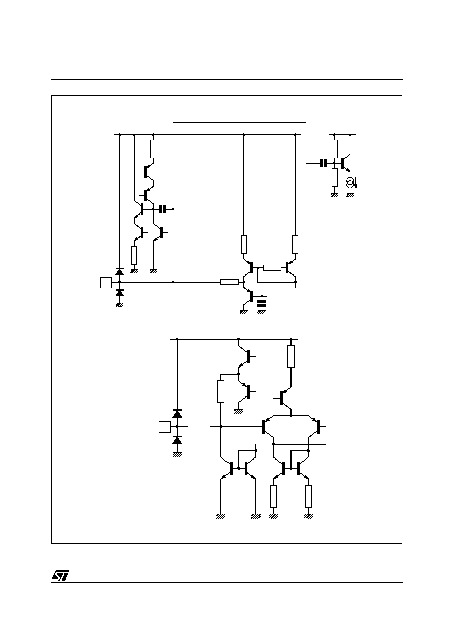
STV223XD/224XC - INPUT/OUTPUT SCHEMATIC DIAGRAMS
59/76
Figure 26. STV2238D (TQFP64) (continued)
INTCVBSOUT
V
CC2
(8V) (Pin 25 - TQFP64)
V
CCIF
(5V)
V
CCIF
(5V) (Pin 20 - TQFP64)
GND
IF
GND
IF
GNDD
GND
IF
GND
IF
GND
IF
GND
IF
GND
IF
GND
IF
EXTAUDIOIN
21
22
(Pin 20 - TQFP64)
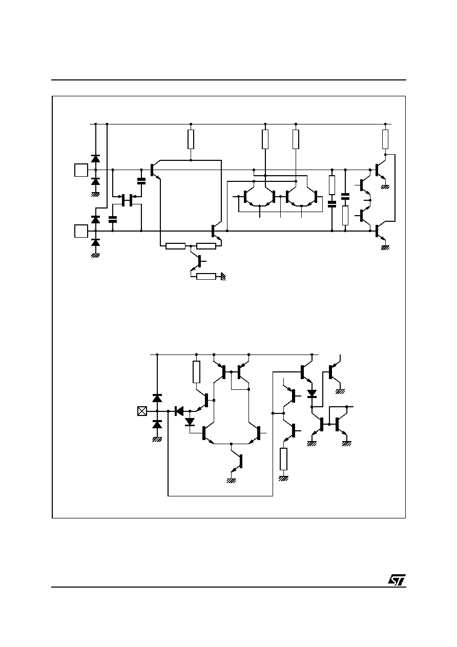
STV223XD/224XC - INPUT/OUTPUT SCHEMATIC DIAGRAMS
60/76
Figure 27. STV2238D (TQFP64) (continued)
CVBS1 - CVBS2
Pins 26 - 28
GND
IF
GND
IF
GND
IF
GND
IF
GND
IF
V
CCIF
(5 V) (Pin 20 - TQFP64)
V
CC1
(8 V) (Pin 59 - TQFP64)
GND2
GND1
GND1
GND1
GND1
GND1
PIFLC1
PIFLC2
24
23
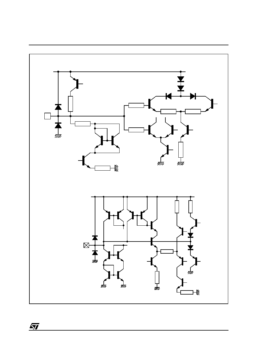
STV223XD/224XC - INPUT/OUTPUT SCHEMATIC DIAGRAMS
61/76
Figure 28. STV2238D (TQFP64) (continued)
BS
BEXT, GEXT, REXT
Pins 30, 31 and 32
V
CC2
(8 V) (Pin 25 - TQFP64)
V
CC2
(8 V) (Pin 20 - TQFP64)
GND2
GND2
GND2
GND2
29
GND2
GND2
GND2
GND2
GND2
GND2
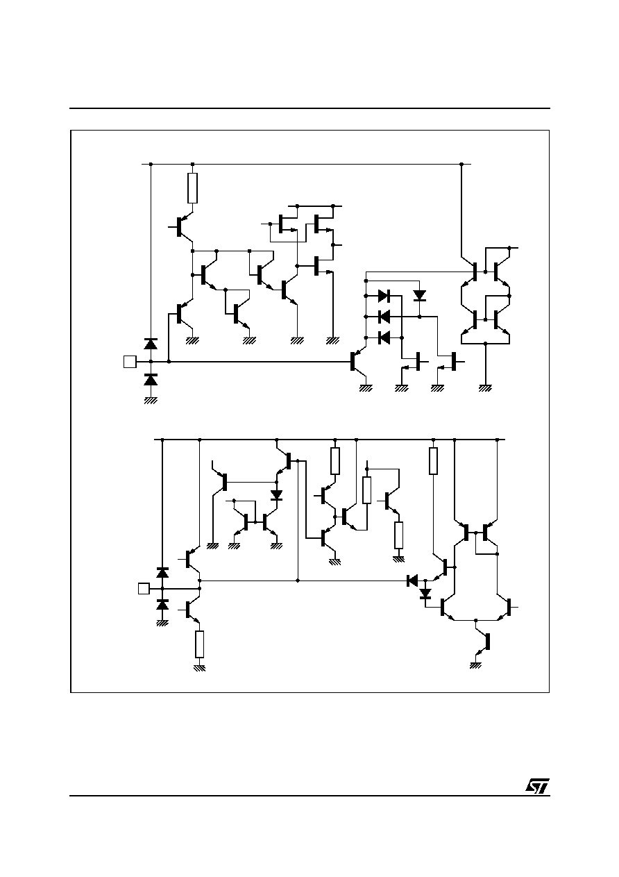
STV223XD/224XC - INPUT/OUTPUT SCHEMATIC DIAGRAMS
62/76
Figure 29. STV2238D (TQFP64) (continued)
FBEXT
Y/CVBS3
V
CC2
(8 V) (Pin 25 - TQFP64)
V
CCD
(5 V) (Pin 4 - TQFP64)
V
CC1
(8 V) (Pin 59 - TQFP64)
GND2
GND2
GND2
GND2
GND2
GND2
GND2
GND2
GND2
33
GND1
GND1
GND1
GND1
GND1
GND2
34
GND1
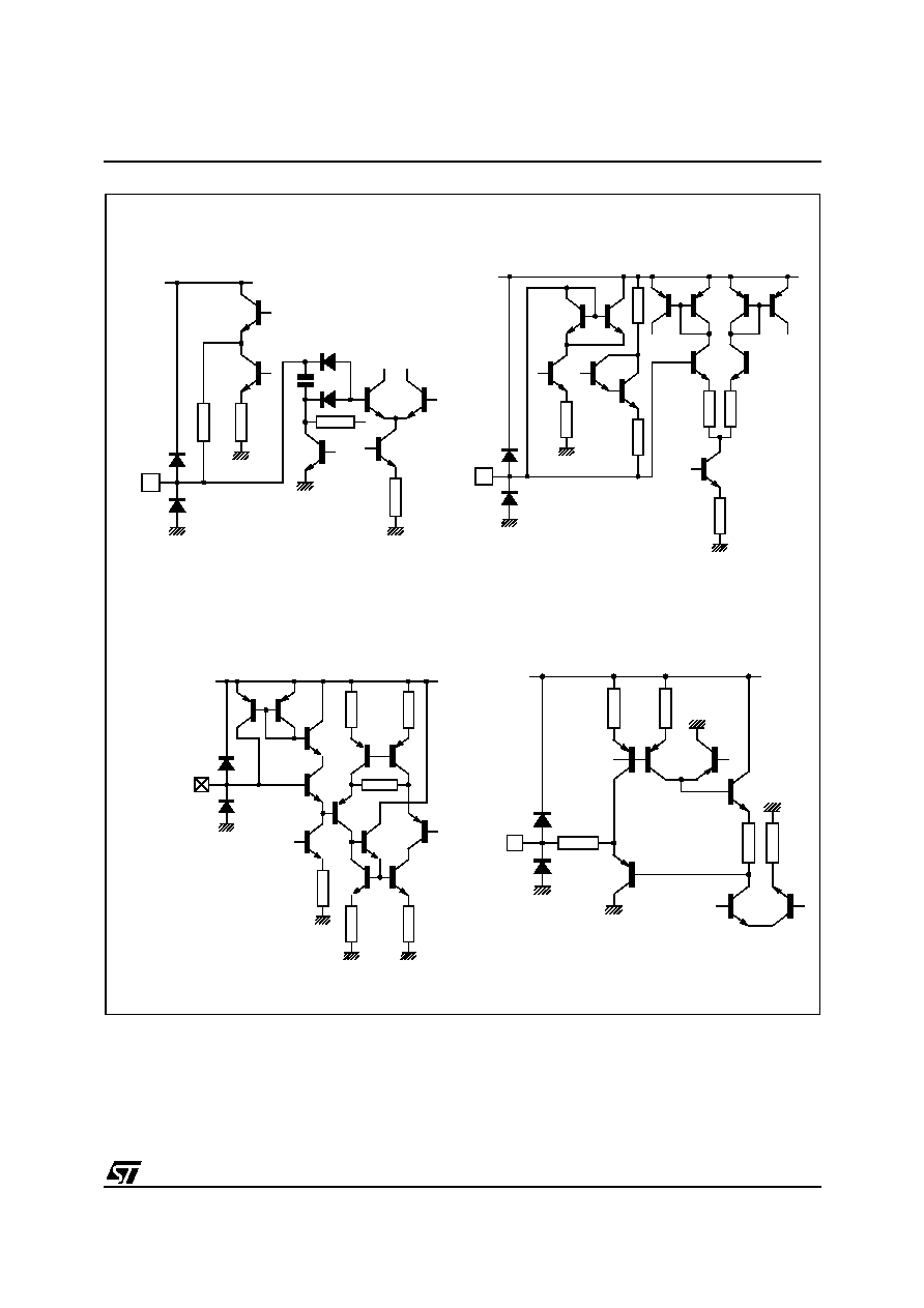
STV223XD/224XC - INPUT/OUTPUT SCHEMATIC DIAGRAMS
63/76
Figure 30. STV2238D (TQFP64) (continued)
V
CC1
(8 V) (Pin 59 - TQFP64)
V
CC2
(8 V) (Pin 25 - TQFP64)
V
CC2
(8 V) (Pin 25 - TQFP64)
UIN, VIN, YIN
Pins 37, 38, 39
V
CC2
(8 V) (Pin 25 - TQFP64)
APR 36
GND2
GND2
GND2
CHR 35
GND2
GND1
GND1
GND1
GND2
GND2
GND2
GND2
GND2
GND2
YOUT 40
GND2
GND2
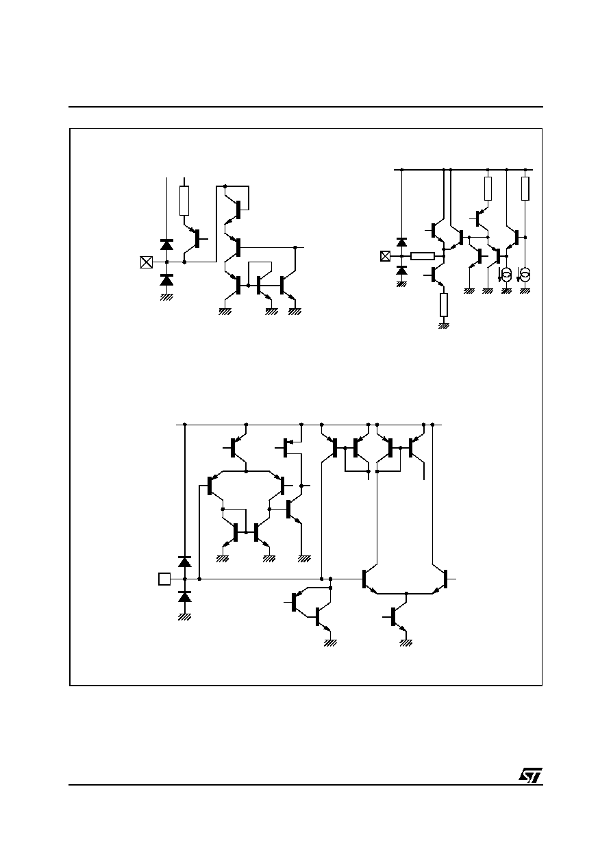
STV223XD/224XC - INPUT/OUTPUT SCHEMATIC DIAGRAMS
64/76
Figure 31. STV2238D (TQFP64) (continued)
BOUT (Pin 43)
GOUT (Pin 44)
ROUT (Pin 45)
V
CC1
(8 V) (Pin 59 - TQFP64)
VOUT, UOUT
Pins 41, 42
V
CC2
(8 V) (Pin 25 - TQFP64)
V
CC2
(8 V) (Pin 25 - TQFP64)
GND2
GND2
GND2
GND2
GND2
GND2
GND2
GND2
GND2
GND2
GND2
GND2
GND2
GND2
I
CATH 46

STV223XD/224XC - INPUT/OUTPUT SCHEMATIC DIAGRAMS
65/76
Figure 32. STV2238D (TQFP64) (continued)
BOSD, GOSD, ROSD
(Pins 47, 48, 49)
FBOSD
V
CC2
(8 V) (Pin 25 - TQFP64)
V
CC2
(8 V) (Pin 25 - TQFP64)
V
CC2
(8 V) (Pin 25 - TQFP64)
HC
GND2
GND2
GND2
GND2
GND2
GND2
50
GND2
GND2
GND2
GND2
GND2
GND2
51
GND2 GND2
GND2
GND2
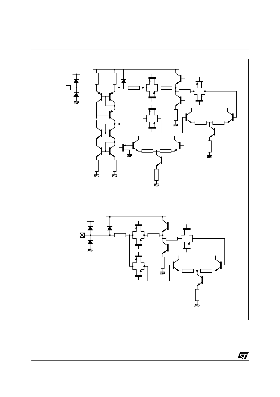
STV223XD/224XC - INPUT/OUTPUT SCHEMATIC DIAGRAMS
66/76
Figure 33. STV2238D (TQFP64) (continued)
XTAL3/BTUN
V
CCD
(5 V) (Pin 4 - TQFP64)
V
CC1
(8 V) (Pin 59 - TQFP64)
V
CC1
(8 V) (Pin 59 - TQFP64)
V
CCD
(5 V) (Pin 4 - TQFP64)
XTAL2, XTAL1
(Pins 53, 54)
GND1
GND1
GND1
GND1
GND1
GND1
GND1
52
GND1
GND1
GND1
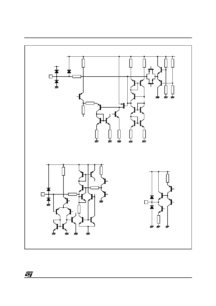
STV223XD/224XC - INPUT/OUTPUT SCHEMATIC DIAGRAMS
67/76
Figure 34. STV2238D (TQFP64) (continued)
CVBSOUT1
V
CCD
(5 V) (Pin 4- TQFP64)
V
CC1
(8 V) (Pin 59 - TQFP64)
V
CC1
(8 V) (Pin 59 - TQFP64)
X1/VAMP/
CHROUT
V
CC1
(8 V) (Pin 59 - TQFP64)
GND1
GND1
GND1
GND1
GND1
GND1
GND1 GND1
GND1
58
GND1
CLPF
GND1
GND1
GND1
GND1
GND1
GND1
GND1
55
56
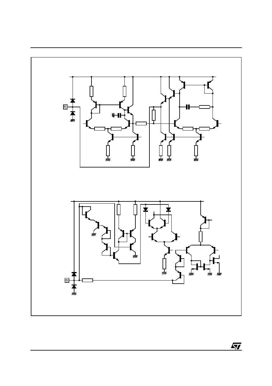
STV223XD/224XC - INPUT/OUTPUT SCHEMATIC DIAGRAMS
68/76
Figure 35. STV2238D (TQFP64) (continued)
CVBSOUT2
BCL/SAF
V
CC1
(8 V) (Pin 59 - TQFP64)
V
CC1
(8 V) (Pin 59 - TQFP64)
GND1
GND1
GND1
GND1
GND1
GND1
GND1
GND1
GND1
GND1
GND1
GND1 GND1
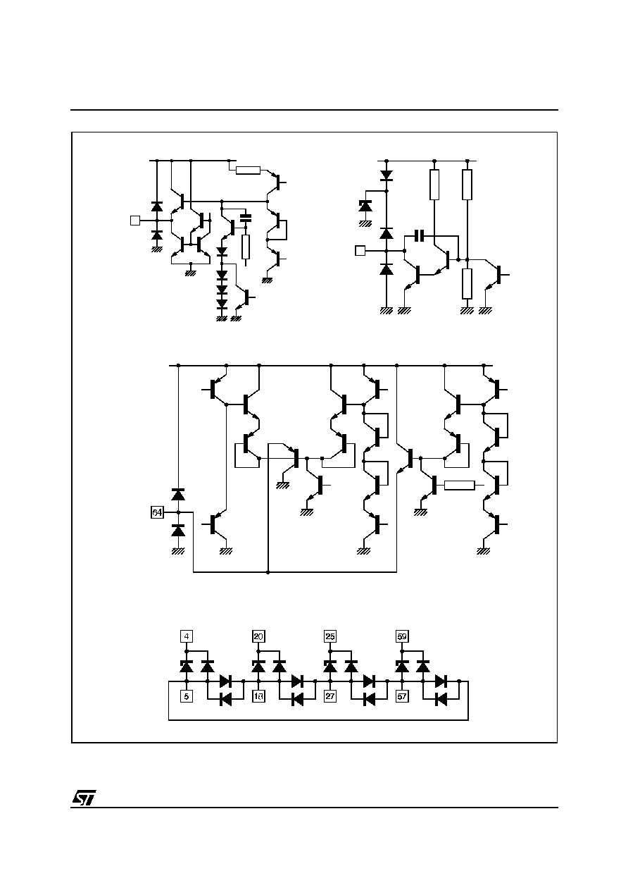
STV223XD/224XC - INPUT/OUTPUT SCHEMATIC DIAGRAMS
69/76
Figure 36. STV2238D (TQFP64) (continued)
LFB/SSC
V
CC1
(8 V) (Pin 59 - TQFP64)
V
CC1
(8 V) (Pin 59 - TQFP64)
V
CC1
(8 V) (Pin 59 - TQFP64)
V
CCD
(5 V)
V
CCIF
(5 V)
V
CC2
(8 V)
V
CC1
(8 V)
GNDD
GND
IF
GND1
GND2
GND1
GND1
GND1
GND1
GND1
GND1
GND1
VERT
GND1
GND1
GND1
GND1
62
HOUT 63
GND1
GND1
GND1
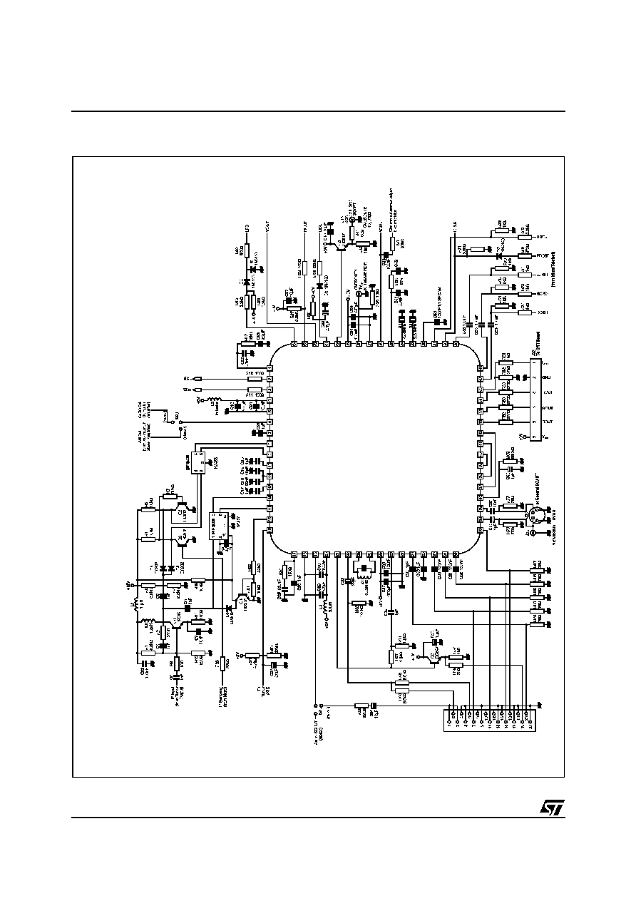
STV223XD/224XC - APPLICATION DIAGRAMS
70/76
9 APPLICATION DIAGRAMS
Figure 37. STV2238D (TQFP64)
1
µF
L
F
B/
SSC
HO
U
T
VE
R
T
BC
L
/
S
A
F
CV
B
S
O
U
T
2
V
CC1
CV
B
S
O
U
T
1
GN
D
1
X1
/
V
AM
P
/
C
H
R
O
U
T
CL
P
F
XT
AL
1
XT
AL
2
XT
AL
3
/
BT
U
N
HC
FB
O
S
D
RO
S
D
IFP
L
L
G
NDI
F
A
M
/F
M
O
U
T
/S
C
V
CCI
F
I
N
T
C
VB
SO
U
T
EXT
AU
D
I
O
I
N
PI
F
L
C
1
PI
F
L
C
2
V
CC2
CV
B
S
I
N
1
G
ND2
CV
B
S
I
N
2
BS
BEX
T
/
C
b
G
E
X
T/Y
R
E
X
T/C
r
GOSD
BOSD
ICATH
ROUT
GOUT
BOUT
UOUT
VOUT
YOUT
YIN
VIN
UIN
APR
CHR
Y/CVBSIN3
FBEXT
SLPF
SCL
SDA
V
CCD
GNDD
AUDIOOUT
FMCAP
SIFIN1
SIFIN2
AGCSIFCAP
V
REFIF
AGCPIFCAP
PIFIN1
PIFIN2
SAW
TUNERAGCOUT
M
U
L
T
I
-
ST
AND
A
RD EUR
O
P
EAN
A
PPL
I
C
A
T
I
O
N
PA
L
/
S
E
C
AM
/
N
TS
C
BG
/
D
K/
I
/
L
L
'
S
T
V2
23
8D
56
k
O
h
m
s
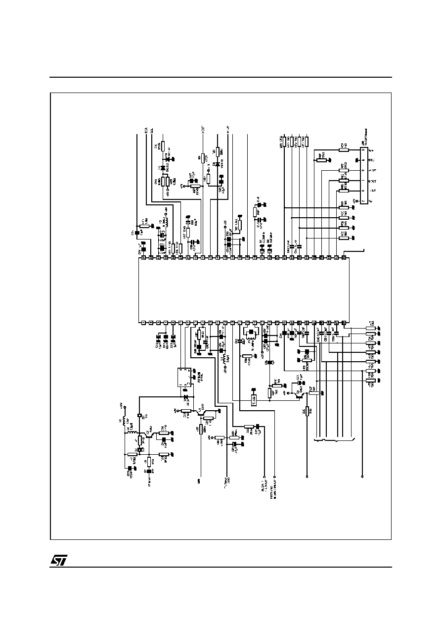
ST
V223XD
/
224XC
-
A
PPL
IC
A
T
ION
D
I
A
G
R
A
M
S
71/
76
F
i
g
u
re 3
8
.
S
T
V
2246
C
MULTISTANDARD ASIA MONO APPLICATION
PAL/NTSC BG/DK/I/M/N
BG/DK/I
27 k Ohm
1 µF
Audio Out
(to audio amplifier)
LFB
BCL
CVBSOUT2
(2 V
PP
)
FBOSD
BOSD
ROSD
GOSD
VAMP
FMCAP
AUDIOOUT
GNDD
V
CCD
SDA
SCL
SLPF
LFB/SSC
HOUT
VERT
BCL/SAF
V
CC1
CVBSOUT2
GND1
X1/VAMP/CHROUT
CLPF
XTAL1
XTAL2
XTAL3
ROSD
GOSD
BOSD
I
CATH
ROUT
GOUT
BOUT
NTBC/CVBSOUT1
NC
NC
NC
V
REFIF
AGCPIFCAP
PIFIN1
PIFIN2
TUNERAGCOUT
IFPLL
GND
IF
FMOUT
V
CCIF
INTCVBSOUT
EXTAUDIOIN
PIFLC1
PIFLC2
V
CC2
CVBSIN1
GND2
CVBSIN2
BS
Y/CVBSIN3
CHR
ARR
BEXT/Cb
GEXT/Y
REXT/Cr
FBEXT
INTCVBSOUT
EXTERNAL CVBS INPUT
FBOSD/HC
From Ext. RGB or
From Ext. YcrCb
SVHS
CVBSOUT1 (1 V
PP
)
S
T
V
2
2
4
6
C
56 kOhms
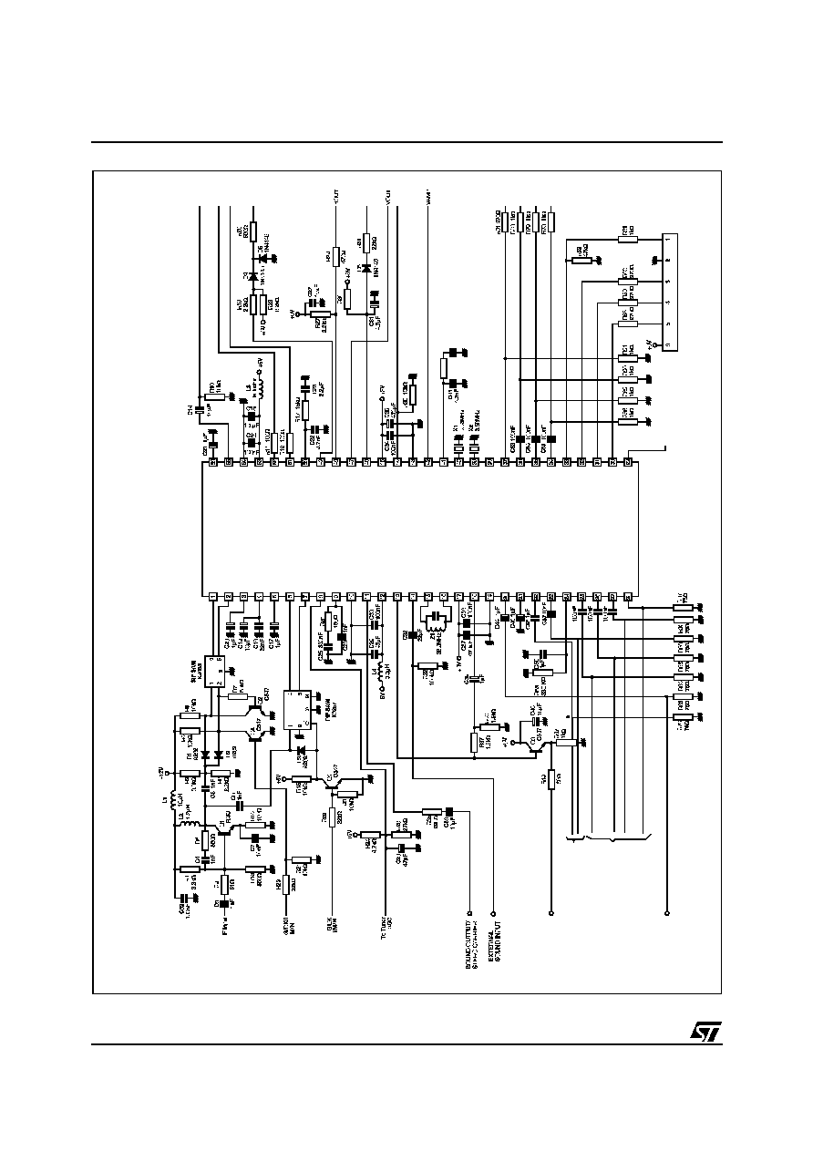
ST
V
223XD
/
224XC
-
A
P
PL
IC
A
T
ION
D
I
A
G
R
A
M
S
72/76
F
i
g
u
re 3
9
.
S
T
V
2247
C
C42
1 µF
R38
FMCAP
AUDIOOUT
GNDD
V
CCD
SDA
SCL
SLPF
LFB/SSC
HOUT
VERT
BCL/SAF
V
CC1
CVBSOUT2
GND1
X1/VAMP/CHROUT
CLPF
XTAL1
XTAL2
XTAL3
ROSD
GOSD
BOSD
I
CATH
ROUT
GOUT
BOUT
NTBC/CVBSOUT1
SIFIN1
SIFIN2
AGCSIFCAP
V
REFIF
AGCPIFCAP
PIFIN1
PIFIN2
TUNERAGCOUT
IFPLL
GND
IF
FMOUT/SC
V
CCIF
INTCVBSOUT
EXTAUDIOIN
PIFLC1
PIFLC2
V
CC2
CVBSIN1
GND2
CVBSIN2
BS
Y/CVBSIN3
CHR
ARR
BEXT/Cb
GEXT/Y
REXT/Cr
FBEXT
INTCVBSOUT
EXTERNAL CVBS INPUT
LFB
Audio Out
(to audio amplifier)
BCL
CVBSOUT
(2 V
PP
)
SDA
SCL
FBOSD
ROSD
GOSD
BOSD
J32
To CRT Board
I
CA
T
H
GN
D
RO
UT
GOU
T
BO
U
T
V
CC
FBOSD/HC
MULTISTANDARD ASIA STEREO APPLICATION
PAL/NTSC BG/DK/I/M/N
S
T
V
2
2
4
7
C
From Ext. RGB or
From Ext. YcrCb
SVHS
CVBSOUT1 (1 V
PP
)
27 kOhms
56 kOhms
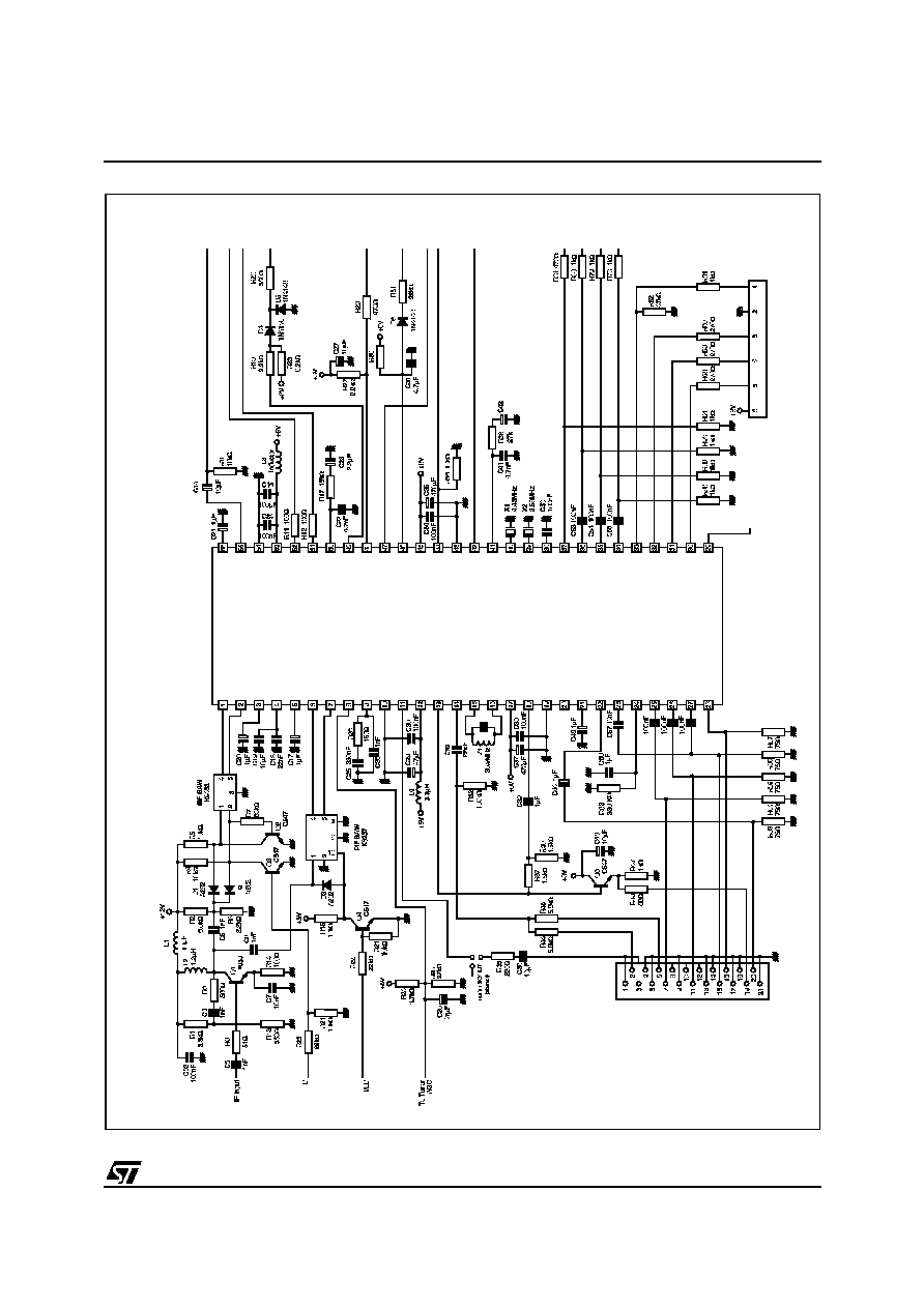
ST
V223XD
/
224XC
-
A
PPL
IC
A
T
ION
D
I
A
G
R
A
M
S
73/
76
F
i
g
u
re 4
0
.
S
T
V
2248
C
BG/DK/I/L
BG/DK
1 µF
I
CA
T
H
GN
D
RO
UT
GOU
T
BO
U
T
V
CC
J32
To CRT Board
FBOSD
ROSD
GOSD
BOSD
Audio Out
(to Audio Amplifier)
SCL
SDA
LFB
BCL
HOUT
VOUT
CVBSOUT
VAMP
FMCAP
AUDIOOUT
GNDD
V
CCD
SDA
SCL
SLPF
LFB/SSC
HOUT
VERT
BCL/SAF
V
CC1
CVBSOUT2
GND1
X1/VAMP/CHROUT
CLPF
XTAL1
XTAL2
XTAL3/BTUN
ROSD
GOSD
BOSD
I
CATH
ROUT
GOUT
BOUT
SIFIN1
SIFIN2
AGCSIFCAP
V
REFIF
AGCPIFCAP
PIFIN1
PIFIN2
TUNERAGCOUT
IFPLL
GND
IF
AM/FMOUT/SC
V
CCIF
INTCVBSOUT
EXTAUDIOIN
PIFLC1
PIFLC2
V
C C2
CVBSIN1
GND2
CVBSIN2
BS
Y/CVBSIN3
CHR
ARR
BEXT/Cb
GEXT/Y
REXT/Cr
FBEXT
FBOSD/HC
MULTI-STANDARD EUROPEAN APPLICATION
PAL/SECAM/NTSC BG/DK/I/LL'
S
T
V
2
2
4
8
C
(2 V
PP
)
NTBC/CVBSOUT1
CVBSOUT1 (1 V
PP
)
56 kOhms
STV223XD/224XC - SUMMARY OF CHANGES
74/76
10 SUMMARY OF CHANGES
Rev.
Main Changes
Date
1.8
Deletion of AM Demodulator for the STV2249C in
Figure 10 on page 14
.
Pin names changed from "NC" to "NTBC" in diagrams.
16 March
2001
1.9
The value of R30 on pin BCL/SAF was changed from 220 kOhms to 56 kOhms in the Application di-
agrams.
Modification of Register 13 in
Section 6.3 STV2238D: Input Signals (Write Mode)
.
Deletion of "PAL/NTSC Only" row of the I≤C Bus Specification table in
Section 7 on page 52
.
12 April
2001
2.0
Modification of Crystal Detection values in
Section 3.2 on page 18
and
CRYSTAL DETECTION on
page 34
. Clarification of POR conditions in
Section 6.5 on page 51
.
8 Jan
2002
2.1
Update of Frequency Control Range value in
Section 4.9 Scanning Part
.
13 Feb
2002
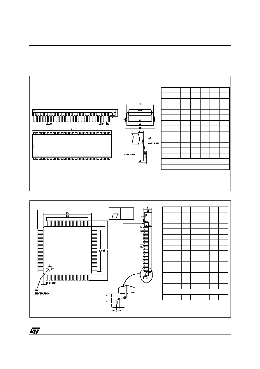
STV223XD/224XC - GENERAL PACKAGE INFORMATION
75/76
11 GENERAL PACKAGE INFORMATION
11.1 PACKAGE MECHANICAL DATA
Figure 41. 56-Pin Shrink Plastic Dual In Line Package, 600-mil Width
Figure 42. 64-Pin Thin Quad Flat Package
A
6.35
0.250
A1
0.38
0.015
A2
3.18
4.95 0.125
0.195
b
0.41
0.016
b2
0.89
0.035
C
0.20
0.38 0.008
0.015
D
50.29
53.21 1.980
2.095
E
15.01
0.591
E1
12.32
14.73 0.485
0.580
e
1.78
0.070
eA
15.24
0.600
eB
17.78
0.700
L
2.92
5.08 0.115
0.200
Number of Pins
N
56
PDIP56S
A
1.60
0.063
A1
0.05
0.15 0.002
0.006
A2
1.35 1.40 1.45 0.053 0.055 0.057
B
0.30 0.37 0.45 0.012 0.015 0.018
C
0.09
0.20 0.004
0.008
D
16.00
0.630
D1
14.00
0.551
D3
12.00
0.472
E
16.00
0.630
E1
14.00
0.551
E3
12.00
0.472
e
0.80
0.031
K
0∞
3.5∞
7∞
L
0.45 0.60 0.75 0.018 0.024 0.030
L1
1.00
0.039
Number of Pins
N
64
ND
16
NE
16
L1
L
K
0.10mm
.004

STV223XD/224XC - GENERAL PACKAGE INFORMATION
76/76
Notes
:
Information furnished is believed to be accurate and reliable. However, STMicroelectronics assumes no responsibility for the consequences
of use of such information nor for any infringement of patents or other rights of third parties which may result from its use. No license is granted
by implication or otherwise under any patent or patent rights of STMicroelectronics. Specifications mentioned in this publication are subject
to change without notice. This publication supersedes and replaces all information previously supplied. STMicroelectronics products are not
authorized for use as critical components in life support devices or systems without the express written approval of STMicroelectronics.
The ST logo is a registered trademark of STMicroelectronics
©
2002 STMicroelectronics - All Rights Reserved.
Purchase of I
2
C Components by STMicroelectronics conveys a license under the Philips I
2
C Patent. Rights to use these components in an
I
2
C system is granted provided that the system conforms to the I
2
C Standard Specification as defined by Philips.
STMicroelectronics Group of Companies
Australia - Brazil - Canada - China - Finland - France - Germany - Hong Kong - India - Israel - Italy - Japan
Malaysia - Malta - Morocco - Singapore - Spain - Sweden - Switzerland - United Kingdom - U.S.A.
http://www.st.com