STV3012
REMOTE CONTROL TRANSMITTER
FOR AUDIO AND VIDEO APPLICATIONS
March 1993
PRELIMINARY DATA
1
2
3
4
5
6
7
8
9
10
20
19
18
17
16
15
14
13
12
11
REMO
SEN6N
SEN5N
SEN4N
SEN3N
SEN2N
SEN1N
SEN0N
ADRM
SS
V
DD
V
DRV6N
DRV5N
DRV4N
DRV3N
DRV2N
DRV1N
DRV0N
OSCO
OSCI
30
12
-
0
1.
E
P
S
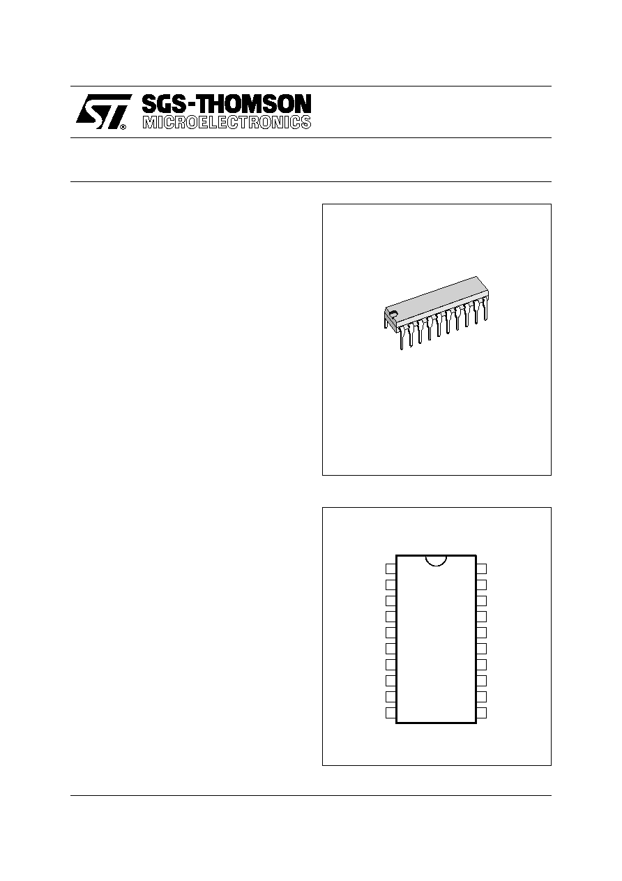
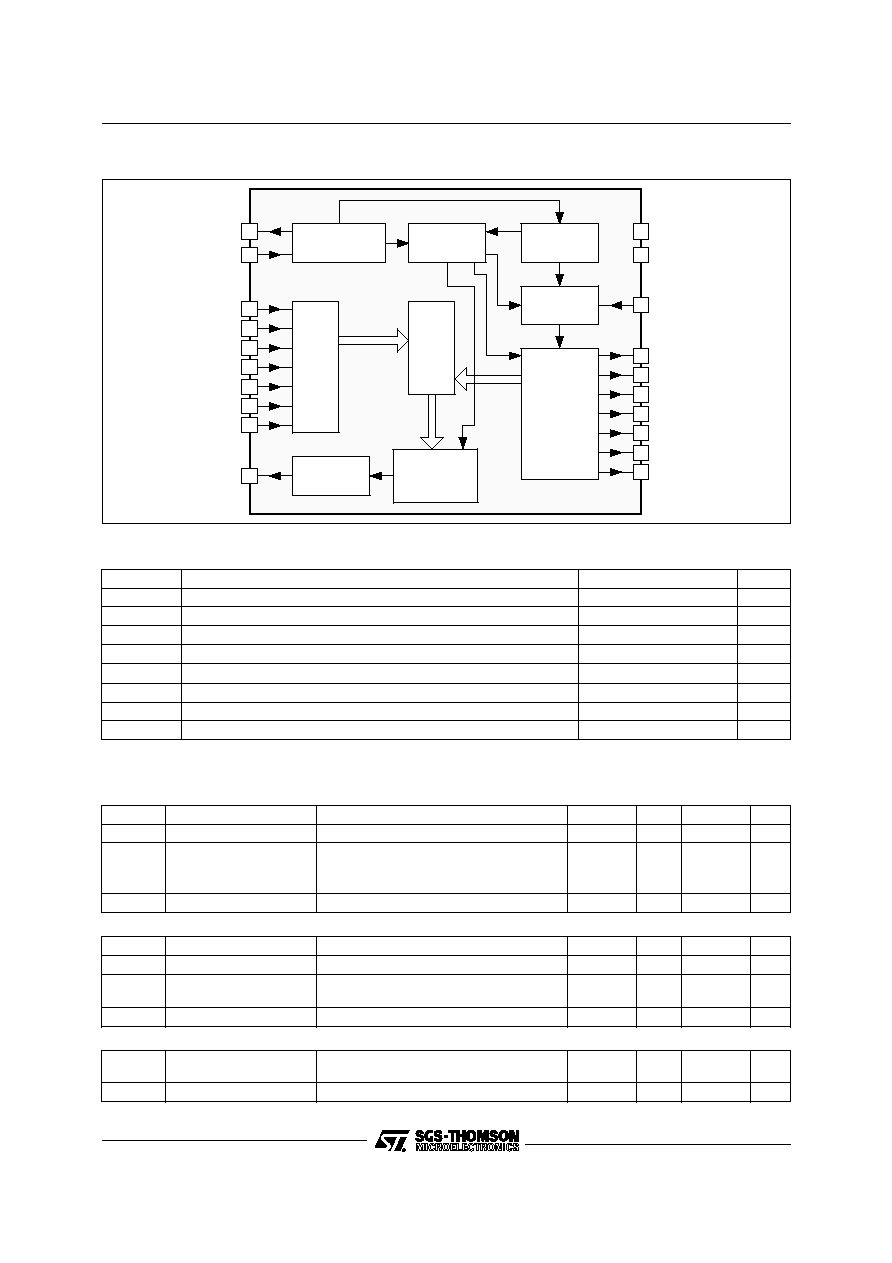
PIN CONNECTIONS
DIP20
(Plastic Package)
ORDER CODE : STV3012
.
TWO TIMING AND DATA FORMAT MODES
.
7 SUB-SYSTEM ADDRESSES
.
UP TO 64 COMMANDS PER SUB-SYSTEM
ADDRESS
.
KEY RELEASE DETECTION BY TOGGLE BIT
(1 toggle bit in mode A and 2 toggle bits in
mode B)
.
HIGH CURRENT REMOTE OUTPUT
AT V
DD
= 3V (-I
OH
= 80mA)
.
VERY LOW STAND-BY CURRENT (< 2
�
A)
.
1mA OPERATIONAL CURRENT AT 6V SUP-
PLY
.
CERAMIC RESONATOR CONTROLLED
FREQUENCY (typ. 450kHz)
.
MODULATED TRANSMISSION
.
SUPPLY VOLTAGE RANGE 2V TO 6.5V
.
LOW NUMBER OF EXTERNAL COMPO-
NENTS
This is advance information on a new product now in development or undergoing evaluation. Details are subject to change without notice.
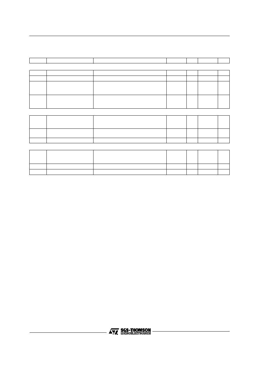
DESCRIPTION
The STV3012 is a general purpose infrared remote
control transmitter system for low voltage supply
applications. It is able to generate a total number
of 448 commands which are divided into 7 sub-sys-
tem groups with 64 commands each. The sub-sys-
tem code may be selected by a press button, a
slider switch or hard wired. Two different timing and
data format modes are available.
1/8
PARALLEL
/SERIAL
CONVERTER
REMOTE
A
DDR
ES
S
LA
TCHE
S
KEYBO
A
R
D
E
NCODE
R
DIVIDER
MASTER
CLEAR
OSCILLATOR
1
2
3
4
5
6
7
8
10
11
12
13
14
15
16
17
18
19
SYST.
CONTR
9
20
K
E
YBO
AR
D
DR
I
V
E
R
D
E
CO
DE
R
OSCO
OSCI
SEN6N
SEN5N
SEN4N
SEN3N
SEN2N
SEN1N
SEN0N
REMO
V
DD
V
SS
ADRM
DRV6N
DRV5N
DRV4N
DRV3N
DRV2N
DRV1N
DRV0N
301
2-
02
.
E
P
S
BLOCK DIAGRAM
ABSOLUTE MAXIMUM RATINGS
Symbol
Parameter
Value
Unit
V
DD
Supply Voltage
- 0.3, 7.0
V
V
I
Input Voltage
- 0.3, V
DD
+ 0.3
V
V
O
Output Voltage
- 0.3, V
DD
+ 0.3
V
�
I
D.C. Current into any input or output
10
mA
- I
(REMO)
Peak REMO Output Current during 10
�
s, duty factor = 1%
300
mA
P
tot
Power Dissipation per package for T
amb
= - 20 to + 70
o
C
200
mW
T
stg
Storage Temperature
- 55, + 125
o
C
T
oper
Operating Ambient Temperature
-20, + 70
o
C
30
12
-
0
1
.
T
B
L
ELECTRICAL CHARACTERISTICS
V
SS
= 0V, T
A
= 25
o
C (unless otherwise specified)
Symbol
Parameter
Test Conditions
Min.
Typ.
Max.
Unit
V
DD
Supply Voltage
T
A
= 0 to + 70
o
C
2
6.5
V
I
DD
Supply Current
�
Active f
OSC
= 455kHz
V
DD
= 3V
REMO Output unload
V
DD
= 6V
0.25
1.0
0.5
2
mA
mA
�
Inactive (stand-by mode)
V
DD
= 6V
2
�
A
f
OSC
Oscill. Frequency
V
DD
= 2 to 6.5V (ceramic resonator)
350
600
kHz
KEYBOARD MATRIX - Inputs SEN0N to SEN6N
V
IL
Input Voltage Low
V
DD
= 2 to 6.5V
0.3 x V
DD
V
V
IH
Input Voltage High
V
DD
= 2 to 6.5V
0.7 x V
DD
V
- I
I
Input Current
V
DD
= 2V, V
I
= 0V
V
DD
= 6.5V, V
I
= 0V
10
100
100
600
�
A
�
A
I
I
Input Leakage Current
V
DD
= 6.5V, V
I
= V
DD
1
�
A
KEYBOARD MATRIX - Outputs DRV0N to DRV6N
V
OL
Output Voltage "ON"
V
DD
= 2V, I
O
= 0.1mA
V
DD
= 6.5V, I
O
= 1.0mA
0.3
0.6
V
V
I
O
Output Current "OFF"
V
DD
= 6.5V, V
O
= 6.5V
10
�
A
30
12
-
0
2
.
T
B
L
STV3012
2/8
ELECTRICAL CHARACTERISTICS
T
amb
= 25
o
C, unless otherwise specified
Symbol
Parameter
Test Conditions
Min.
Typ.
Max.
Unit
CONTROL INPUT ADRM
V
IL
Input Voltage Low
0.3 x V
DD
V
V
IH
Input Voltage High
0.7 x V
DD
V
I
IL
Input Current Low
(switched P and N
channel pull-up/pull down)
Pull-up Act. Oper. Condition, V
IN
= V
SS
V
DD
= 2V
V
DD
= 6.5V
-10
-100
-100
-600
�
A
�
A
I
IH
Input Current High
(switched P and N
channel pull-up/pull down)
Pull-down Act. Stand-by Cond.,V
IN
= V
DD
V
DD
= 2V
V
DD
= 6.5V
10
100
100
600
�
A
�
A
DATA OUTPUT REMO
- I
OH
Output Current High
V
DD
= 2.5V, V
OH
= 0.8V, T
A
= 70
o
C
V
DD
= 2.5V, V
OH
= 0.8V, T
A
= 25
o
C
V
DD
= 6.5V, V
OH
= 5V
70
80
80
mA
mA
mA
I
OL
Output Current Low
V
DD
= 2V, V
OL
= 0.4V
V
DD
= 6.5V, V
OL
= 0.4V
0.6
0.6
mA
mA
t
OH
Pulse Length
V
DD
= 6.5V, Oscill. Stopped
1
msec
OSCILLATOR
I
I
Input Current
OSCI at V
DD
V
DD
= 2V
V
DD
= 6.5V
5
5
7
�
A
�
A
V
OH
Output Voltage high
V
DD
= 6.5V, - I
OH
= 0.1mA
V
DD
- 0.8
V
V
OL
Output Voltage Low
V
DD
= 6.5V, I
OL
= 0.1mA
0.7
V
30
12
-
0
3
.
T
B
L
I - INPUTS AND OUTPUTS
I.1 - Key Matrix Inputs and Outputs (DRV0N to
DRV6N and SEN0N to SEN6N)
The transmitter keyboard is arranged as a scanned
matrix. The matrix consists of 7 driver ouputs and
7 sense inputs. The driver outputs DRV0N to
DRV6N are open drain N-channel transistors and
they are conductive in the stand-by mode. The 7
sense inputs (SEN0N to SEN6N) enable the gen-
eration of 56 command codes. With 2 external
diodes all 64 commands are addressable. The
sense inputs have P-channel pull-up transistors so
that they are HIGH until they are pulled LOW by
connecting them to an output via a key depression
to initiate a code transmission. The codes for the
selected key are given in Table 1.
I.2 - Address Mode Input (ADRM)
The sub-system address and the transmission
mode are defined by connecting the ADRM input
to one or more driver outputs (DRV0N to DRV6N)
of the key matrix. If more than one driver is con-
nected to ADRM, they must be decoupled by di-
odes. This allows the definition of seven
sub-system addresses as shown in Table 2.
The ADRM input has switched pull-up and pull-
down loads. In the stand-by mode only the pull-
down device is active. Whether ADRM is open
(sub-system address 0) or connected to the driver
outputs, this input is LOW and will not cause un-
wanted dissipation. When the transmitter becomes
active by pressing a key, the pull-down device is
switched-off and the Pull-up device is switched-on,
so that the applied driver signals are sensed for the
decoding of the sub-system address and the mode
of transmission.
The arrangement of the sub-system address cod-
ing is such that only the driver DRVnN with the
highest number (n) defines the sub-system ad-
dress, e.g. in mode B, if drivers DRV2N and DRV4N
are connected to ADRM, only DRV4N will define
the sub-system address. This option can be used
in systems requiring more than one sub-system
address. The transmitter may be hard-wire for sub-
system address 2 by connecting DRV1N to ADRM.
If now DRV3N is added to ADRM by a key or a
switch, the transmitted sub-system address
changes to 4. A change of the sub-system will not
start a transmission.
I.3 - Remote Control Signal Output (REMO)
The REMO signal output stage is a push-pull type.
In the HIGH state, a bipolar emitter-follower allows
a high output current. The timing of the data output
format is listed in Figures 1 and 2.
STV3012
3/8
The information is defined by the first edge of the
modulated pulses. During mode A, the data word
starts with the four bits for defining the sub-system
address S3, S2, S1 and S0, followed by the toggle
bit T0, and seven bits G, F, E, D, C, B and A, which
are defined by the selected key. During mode B,
the data word starts with the Toggle bits T1 and T0,
followed by three bits for defining the sub-system
address S2, S1 and S0, and six bits F, E, D, C, B
and A which are defined by the selected key.
The toggle bits function as an indication for the
decoder that the next instruction has to be consid-
ered as a new command.
The REMO output is protected against "lock-up",
i.e. the length of an output pulse is limited to
< 1msec, even if the oscillator stops during an
output pulse. This avoids the rapid discharge of the
battery that would otherwise be caused by the
continuous activation of the LED.
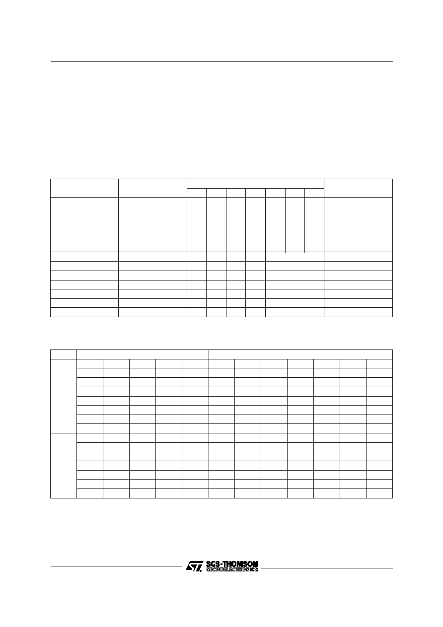
Table 1 : Key Codes
Matrix
Drive
Matrix
Sense
Code
Matrix
Position
G**
F
E
D
C
B
A
DRV0N
DRV1N
DRV2N
DRV3N
DRV4N
DRV5N
DRV6N
V
SS
SEN0N
SEN0N
SEN0N
SEN0N
SEN0N
SEN0N
SEN0N
SEN0N
0
0
0
0
0
0
0
0
0
0
0
0
0
0
0
0
0
0
0
0
0
0
0
0
0
0
0
0
0
0
0
0
0
0
0
0
1
1
1
1
0
0
1
1
0
0
1
1
0
1
0
1
0
1
0
1
0
1
2
3
4
5
6
7
DRV0N to V
SS
SEN1N
0
0
0
1
*
8 to 15
DRV0N to V
SS
SEN2N
0
0
1
0
*
16 to 23
DRV0N to V
SS
SEN3N
0
0
1
1
*
24 to 31
DRV0N to V
SS
SEN4N
0
1
0
0
*
32 to 39
DRV0N to V
SS
SEN5N
0
1
0
1
*
40 to 47
DRV0N to V
SS
SEN6N
0
1
1
0
*
48 to 55
DRV0N to V
SS
SEN5N and SEN6N
0
1
1
1
*
56 to 63
* The C, B and A codes are identical to SEN0N as given above.
** Bit position G only available in mode A.
30
12
-
0
5
.
T
B
L
Table 2 : Transmission Mode and Sub-system Address Selection
Mode
Sub-system Address
Driver DRVnN for n =
M
O
D
E
A
#
S3
S2
S1
S0
0
1
2
3
4
5
6
0
0
0
0
0
1
0
0
1
0
X
X
X
X
X
O
2
0
1
1
0
X
X
X
X
O
3
0
0
0
1
X
X
X
O
4
0
1
0
1
X
X
O
5
0
0
1
1
X
O
6
0
1
1
1
O
M
O
D
E
B
0
1
1
1
O
1
0
0
0
O
O
2
0
0
1
X
O
O
3
0
1
0
X
X
O
O
4
0
1
1
X
X
X
O
O
5
1
0
0
X
X
X
X
O
O
6
1
0
1
X
X
X
X
X
O
O
O
= connected to ADRM
blank
= not connected to ADRM
X
= don't care
The sub-system address and the transmission mode are defined by connecting the ADRM input to one or more driver outputs (DRV0N to
DRV6N) of the key matrix. If more than one driver is connected to ADRM, they must be decoupled by diodes.
30
12
-
0
4
.
T
B
L
STV3012
4/8
t
w
H
L
REMO
S3
0
S2
1
1
S0
0
S1
1
G
0
T0
F
0
E
0
D
1
C
0
B
0
S3
bit
data
A
bit
T0
0
0
B
1
C
0
D
0
E
S0
0
F
1
S2
0
S1
1
1
T1
REMO
L
H
data
t
w
A
1
T0
MODE B
MODE A
0
3
0
1
2
-0
3
.
EP
S
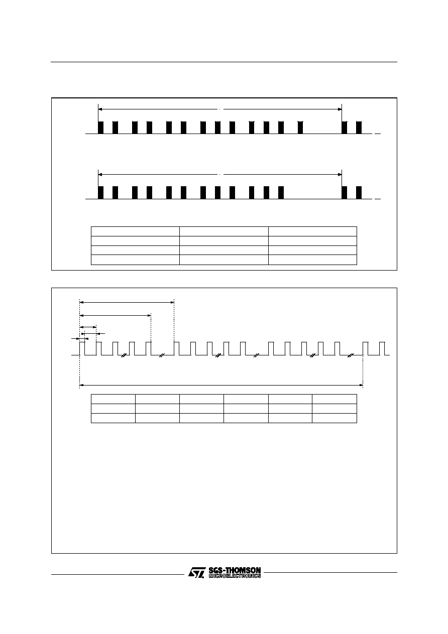
Figure 1 :
Data Format of REMO ; T0 and T1 = toggle bits ; S0, S1, S2 and S3 = sub-system address ;
A, B, C, D, E, F and G = command bits
t
MH
t
ML
t
M
t
PW
t
B
(bit duration)
1st bit
2nd bit
last bit
t
W
(word distance)
3
0
1
2
-0
4
.
EPS
Figure 2 : Pulse Train Timing (ref. to f
OSC
= 400kHz)
Bit Separation (t
B
)
Mode A
Mode B
Logic "0"
1 x t
0
2 x t
0
Logic "1"
2 x t
0
3 x t
0
Toggle bit time
1 x t
0
or 2 x t
0
2 x t
0
or 3 x t
0
Mode
t
0
(ms)
t
M
(
�
s)
t
MH
(
�
s)
t
ML
(
�
s)
t
W
(ms)
A
2.52
30
10
20
86.04
B
2.88
30
10
20
138
Mode A and B
t
OSC
2.5
�
s
oscillation period
t
M
12 x t
OSC
modulation period
t
ML
8 x t
OSC
modulation period LOW
t
MH
4 x t
OSC
modulation period HIGH
Mode A
t
PW
(15 x t
M
) + t
MH
modulated pulse
t
0
1008 x t
OSC
basic unit of pulse distance
t
W
34416 x t
OSC
word distance
Mode B
t
PW
(11 x t
M
) + t
MH
modulated pulse
t
0
1152 x t
OSC
basic unit of pulse distance
t
W
55296 x t
OSC
word distance
STV3012
5/8