 | ÐлекÑÑоннÑй компоненÑ: STV3550 | СкаÑаÑÑ:  PDF PDF  ZIP ZIP |
Äîêóìåíòàöèÿ è îïèñàíèÿ www.docs.chipfind.ru
DATASHEET
This is preliminary information on a new product now in development. Details are subject to change without notice.
February 2004
Revision 1.3
DMS No. 03688M
1/144
STV3550
LCD and Matrix Display TV Processor
®
Main Features
Fully-programmable Digital Video Output Stage for direct
RGB interface to Flat Display Panel with 4- to 10-bit color
resolution and pixel resolution from VGA to WXGA including
HDTV2.
Versatile Integrated Up-Converter
50/60-Hz Progressive output with Line-Interpolation
(A + A*), Field-Merging (A + B) or with Motion-adaptive
De-interlacing based on median f(A, B)
Advanced Still Picture modes: AA*AA* and ABAB
interlaced or AAAA non-interlaced
Automatic Movie mode detection and scanning
Standard Definition Input
ITU-R BT.656/601 Video Input
Separate H/V inputs synchronous with input clock
3D Temporal Noise Reduction with Comet-effect
Correction
Movie Mode Detection with Motion Phase Recovery
Scene-change Detector for Contrast Enhancer and Up-
conversion Control
Letterbox Format Detection and Auto-Format Correction
High-Quality Video Display
Picture Structure Improvement including Color Transition
Improvement, Luma Peaking/Coring and Luma Contrast
Enhancer
H/V format conversion with Zoom In/Out (4x to 1/8x) with
H/V decimation
Letterbox and 4:3 to 16:9 format conversion with
programmable 5-segment Panoramic mode
Very flexible Sync Generator for Master and Slave
modes by Vsync and Hsync signals generation
Progressive Display mode (60 Hz, 50 Hz) for full-screen
graphic planes
Mosaic mode with up to 16 pictures displayed
Picture Compositor to provide Transparency mode between
Video and Graphic planes
High-Performance 8-bit Bitmap OSD Generator
Pixel-based resolution with 10-bit RGB outputs
Programmable Resolution up to WXGA, all standard
displays are supported:
-
Teletext 1.5 (480x520) and 2.5 (672x520)
-
Double-page Teletext (960x520) with Picture-and-Text
-
TeleWeb (640x480)
4 graphic planes with full alpha-blending capabilities:
-
24-bit Background Plane
-
10-bit RGB Video Plane
-
Bitmap OSD Plane with Color Map
-
Up to 128 x 128 pixel Cursor Plane
2D Graphics Accelerator
Embedded 32-bit ST20 CPU Core
Peripherals and I/Os for TV Chassis Control:
30 fully-programmable I/Os (5V tolerant)
4 external interrupts
8-bit programmable PWM with 4 inputs/outputs
Infrared Digital Preprocessor
Real Time Clock and Watchdog Timer
4 16-bit standard timers
10-bit ADC with 6 inputs and wake-up capability
2 Master/Slave I²C Bus Interfaces
UART and support for IrDA interfaces
Teletext 1.5 and 2.5, Closed-Caption, VPS and
WSS VBI Data Decoding, TeleWeb Compliant
Embedded Emulation Resources with In-Situ
Flash Programming Capabilities
1.8V and 3.3V Power supplies
Eco Standby mode
27-MHz Crystal Oscillator
PC input compatible
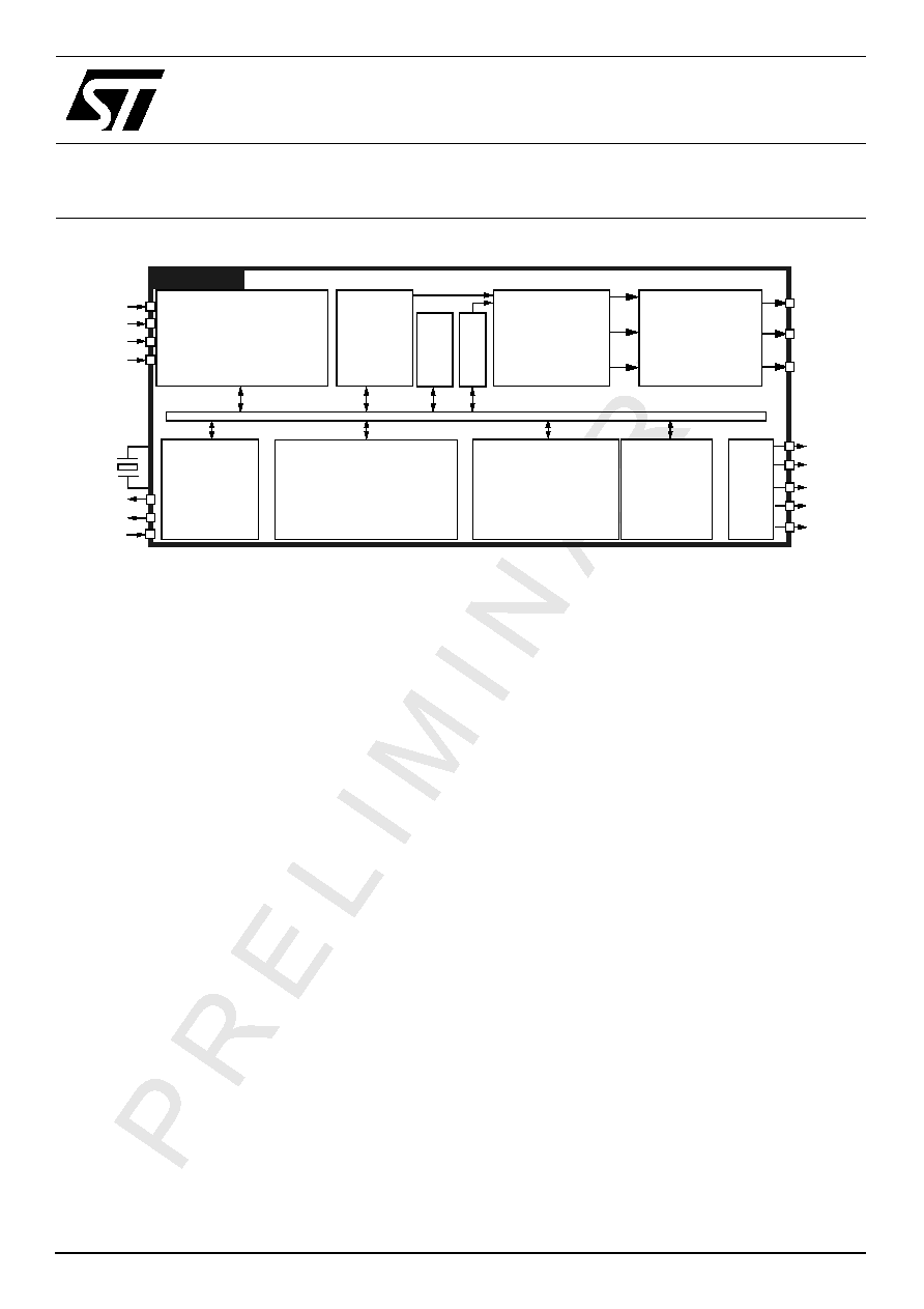
H100
V100
Output
YCRCB[7:0]
VSYNC
Clock
Generator
2D
B
l
o
ck
OSD
STV3550
Mo
ve
HSYNC
27 MHz
CLK_DATA
CLKXTM
CLKXTP
Clock
External
Memory
Interface
Flash
SDRAM
Video
Display
Pipeline
PSI/CTI
Standard Definition
Input (SDIN)
H/V Filter
Temporal Noise Reduction
Film Mode Detection
Picture
Compositor
Cursor Plane
Background Plane
Gamma Correction
Digital
Video
Output
Perfect Color
Engine
TV Peripherals
RTC, ADC, I²C Bus,
I/O Ports, 4 Timers,
UART, WDT, PWM
and Infrared Digital
Preprocessor
DCLK
DE
Ti
m
e
b
a
s
e
Ge
ne
r
a
tor
RGB Digital
Video
Outputs
Reset
4 to 10-bit
ST20 32-bit CPU Core
4 kB I-Cache 4 kB D-Cache
Interrupt Controller
Diagnostic Controller
100 MHz, 8 kB SRAM

2/144
STV3550
Chapter 1
General Information . . . . . . . . . . . . . . . . . . . . . . . . . . . . . . . . . . . . . . . . . . . . . . . .7
1.1
Introduction .......................................................................................................................... 7
1.2
Software ............................................................................................................................... 8
1.3
Related Documentation ...................................................................................................... 10
1.3.1
General Introduction Manual ................................................................................................................10
1.3.2
User Guides ..........................................................................................................................................10
1.3.3
Reference Guide ..................................................................................................................................11
Chapter 2
STV3550 Pin List . . . . . . . . . . . . . . . . . . . . . . . . . . . . . . . . . . . . . . . . . . . . . . . . .12
2.1
Pinout ................................................................................................................................ 12
2.2
Pin Description .............................................................................................................. 13
2.3
Parallel I/O Pins and Alternate Functions .......................................................................... 19
Chapter 3
Video Functional Description . . . . . . . . . . . . . . . . . . . . . . . . . . . . . . . . . . . . . . .20
3.1
Standard Definition Input (SDIN) ........................................................................................ 20
3.1.1
System Description ...............................................................................................................................20
3.2
Video Timebase Generator (VTG) ..................................................................................... 22
3.2.1
Synchronization Modes ........................................................................................................................22
3.2.2
Deinterlacing Modes and Progressive Scan Output .............................................................................22
3.2.3
Regulation Modes .................................................................................................................................23
3.3
Video Display Pipeline ....................................................................................................... 24
3.3.1
Main Features .......................................................................................................................................25
3.3.2
Horizontal and Vertical Rescaling ........................................................................................................25
3.3.3
Image Improvement ..............................................................................................................................27
3.3.4
Brightness Estimator ............................................................................................................................28
3.3.5
Histogram .............................................................................................................................................28
3.3.6
Contrast Enhancer ................................................................................................................................28
3.3.7
Spectral Processing ..............................................................................................................................35
3.3.8
Color Transient Improvement ...............................................................................................................36
Chapter 4
Graphics Functional Description . . . . . . . . . . . . . . . . . . . . . . . . . . . . . . . . . . . .37
4.1
On-Screen Display Generator (OSD) ................................................................................. 37
4.1.1
General Information ..............................................................................................................................37
4.1.2
Main Features .......................................................................................................................................37
4.1.3
Functional Description ..........................................................................................................................37
4.1.4
Programming OSD Display Regions ....................................................................................................38
4.1.5
Mixing OSD and Video Signals .............................................................................................................48
4.2
2D Graphics Accelerator .................................................................................................... 49
4.3
Graphic Application Examples ........................................................................................... 50
4.3.1
Teletext 1.5 ...........................................................................................................................................50
4.3.2
Teletext Level 2.5 ..................................................................................................................................51
4.3.3
TeleWeb ................................................................................................................................................51
4.4
Picture Compositor ............................................................................................................. 53

STV3550
3/144
4.4.1
Background Color Plane .......................................................................................................................54
4.4.2
Video Plane ..........................................................................................................................................54
4.4.3
Cursor Plane .........................................................................................................................................54
4.4.4
Graphics Plane .....................................................................................................................................54
Chapter 5
Output Stage . . . . . . . . . . . . . . . . . . . . . . . . . . . . . . . . . . . . . . . . . . . . . . . . . . . . .56
5.1
Color Space Adaptor (CSA) and Interpolator ..................................................................... 56
5.1.1
Main Features .......................................................................................................................................56
5.1.2
General Description ..............................................................................................................................56
5.1.3
Up-sampling .........................................................................................................................................56
5.1.4
GFX_ACTIVE Signal ............................................................................................................................57
5.2
Gamma Correction ............................................................................................................. 59
5.3
Perfect Color Engine .......................................................................................................... 59
5.4
Digital Video Output Stage ................................................................................................. 59
5.4.1
Introduction ...........................................................................................................................................59
5.4.2
Vsync Output Capability .......................................................................................................................60
5.4.3
Hsync Output Capability .......................................................................................................................60
5.4.4
Csync Output Capability .......................................................................................................................60
5.4.5
RGB Output ..........................................................................................................................................60
5.4.6
Data Enable Output ..............................................................................................................................64
5.4.7
Data Clock Output ................................................................................................................................65
5.4.8
Pad Control ...........................................................................................................................................65
5.4.9
Register ................................................................................................................................................65
Chapter 6
CPU and System Management Functional Description . . . . . . . . . . . . . . . . . .66
6.1
ST20 C2C200 CPU Core ................................................................................................... 66
6.1.1
General Information ..............................................................................................................................66
6.1.2
Main Features .......................................................................................................................................66
6.2
ST Bus Interconnect Overview ........................................................................................... 66
6.3
STV3550 Memory Interface ............................................................................................... 66
6.3.1
Memory Devices ...................................................................................................................................66
6.3.2
Configuring the STV3550 Memory Interface during Boot .....................................................................67
6.3.3
Address Format ....................................................................................................................................67
6.3.4
Control Registers ..................................................................................................................................67
6.3.5
Memory Configurations ........................................................................................................................68
6.3.6
Clock Management and Timing Issues .................................................................................................68
6.3.7
STV3550 Memory Interfaces ................................................................................................................68
6.3.8
STV3550 Memory Interface Capabilities Regarding Flash Device .......................................................69
6.3.9
STV3550 Memory Interface Capabilities Regarding SDRAM Device ...................................................71
6.3.10
SDRAM Low Power Mode ....................................................................................................................75
6.3.11
Memory Configurations ........................................................................................................................76
6.3.12
STV3550 External and Internal Memory Mapping ................................................................................81
6.4
Reset Strategy ................................................................................................................... 81

4/144
STV3550
6.4.1
External Hard Reset .............................................................................................................................81
6.4.2
Internal Reset Generated by the Watchdog .........................................................................................82
6.4.3
Internal Soft Reset ................................................................................................................................82
6.5
Booting the STV3550 ......................................................................................................... 82
6.5.1
Typical Boot Sequence .........................................................................................................................82
6.5.2
Starting The Main Application Program ................................................................................................83
6.6
Standby Mode .................................................................................................................... 83
6.7
Interrupt Management ........................................................................................................ 84
6.8
Clock Generator ................................................................................................................. 85
Chapter 7
TV Chassis Control . . . . . . . . . . . . . . . . . . . . . . . . . . . . . . . . . . . . . . . . . . . . . . .86
7.1
PWM and Counter Module ................................................................................................. 86
7.1.1
External Interface ................................................................................................................................86
7.1.2
PWM Functions ....................................................................................................................................86
7.1.3
Counter Functions ................................................................................................................................87
7.2
Infrared Receiver Preprocessor ......................................................................................... 88
7.3
Watchdog Timer (WDT) ..................................................................................................... 89
7.3.1
Clearing the Counter ............................................................................................................................89
7.3.2
Generation of Internal Watchdog Reset Signal ....................................................................................90
7.4
Real Time Clock (RTC) ...................................................................................................... 91
7.4.1
Real Time Clock (RTC) .........................................................................................................................91
7.5
Basic Timer ........................................................................................................................ 92
7.5.1
Functional Description ..........................................................................................................................92
7.5.2
Interrupt Selection ................................................................................................................................93
7.6
Analog to Digital Converter ................................................................................................ 94
7.6.1
Introduction ...........................................................................................................................................94
7.6.2
Main Features .......................................................................................................................................94
7.6.3
General Description ..............................................................................................................................94
7.6.4
Analog Watchdog .................................................................................................................................95
7.6.5
Low Power Modes ................................................................................................................................96
7.7
Inter Integrated Circuit Bus (I²C) ........................................................................................ 97

STV3550
5/144
7.7.1
Basic Features ......................................................................................................................................97
7.7.2
Functional Description ..........................................................................................................................97
7.7.3
PIO Pad Connection & Control .............................................................................................................98
7.7.4
Clock Generation ..................................................................................................................................99
7.7.5
Clock Control ........................................................................................................................................99
7.7.6
Shift Register ......................................................................................................................................101
7.7.7
Clock Edge Detection .........................................................................................................................102
7.7.8
Receive Data Sampling ......................................................................................................................103
7.7.9
Transmit & Receive Buffers ................................................................................................................104
7.7.10
Loopback Mode ..................................................................................................................................104
7.7.11
Enabling Operation .............................................................................................................................104
7.7.12
Master/Slave Operation ......................................................................................................................104
7.7.13
Error Detection ...................................................................................................................................105
7.7.14
Interrupt Mechanism ...........................................................................................................................106
7.7.15
Software Reset ...................................................................................................................................106
7.7.16
I²C Operation ......................................................................................................................................107
7.7.17
Clock Period In I²C Mode ...................................................................................................................109
7.7.18
Clock Synchronization ........................................................................................................................110
7.7.19
START/STOP Condition Detection ..................................................................................................... 111
7.7.20
Slave Address Comparison ................................................................................................................ 111
7.7.21
Clock Stretching ..................................................................................................................................112
7.7.22
START/STOP Condition Generation .................................................................................................. 112
7.7.23
Acknowledge Bit Generation ..............................................................................................................113
7.7.24
Arbitration Checking ...........................................................................................................................113
7.7.25
I²C Timing Specification ......................................................................................................................114
7.8
Asynchronous Serial Controller (ASC) ............................................................................. 116
7.8.1
Control ................................................................................................................................................116
7.8.2
Data Frames .......................................................................................................................................117
7.8.3
Transmission ......................................................................................................................................118
7.8.4
Reception ...........................................................................................................................................119
7.8.5
Baud Rate Generation ........................................................................................................................121
7.8.6
Interrupt Control ..................................................................................................................................123
7.9
IrDA Encoder/Decoder ..................................................................................................... 126
7.9.1
Encoding Scheme ..............................................................................................................................126
7.9.2
Decoding Scheme ..............................................................................................................................126
7.9.3
Register ..............................................................................................................................................127
Chapter 8
General Package Information . . . . . . . . . . . . . . . . . . . . . . . . . . . . . . . . . . . . . .128
8.1
Package Mechanical Data ............................................................................................. 128
Chapter 9
Electrical Characteristics . . . . . . . . . . . . . . . . . . . . . . . . . . . . . . . . . . . . . . . . .130
9.1
Absolute Maximum Ratings ............................................................................................ 130
9.2
Thermal Data .................................................................................................................. 131
9.3
DC Electrical Characteristics ............................................................................................ 131
9.4
Supply Current Characteristics ....................................................................................... 132
9.5
H/V Synchronization Characteristics ............................................................................... 132
Document Outline