 | –≠–ª–µ–∫—Ç—Ä–æ–Ω–Ω—ã–π –∫–æ–º–ø–æ–Ω–µ–Ω—Ç: STV5109 | –°–∫–∞—á–∞—Ç—å:  PDF PDF  ZIP ZIP |
September 2003
1/7
STV5109
RGB HIGH VOLTAGE VIDEO AMPLIFIER
s
Bandwidth : 8MHz typical
s
Supply Voltage : 220V typical
s
Rise and Fall Time : 50ns TYPICAL
s
CRT Cathode Current Outputs for Parallel or
Sequential Cut-off or Drive Adjustment
s
Flashover Protection
DESCRIPTION
The STV5109 includes three video amplifiers
desi-gned with a high voltage bipolar/CMOS/
DMOS technology (BCD). It drives directly the
three cathodes and is protected against
flashovers. Thanks to its three cathode current
outputs, the STV5109 can be used with both par-
allel and sequential sampling applications.
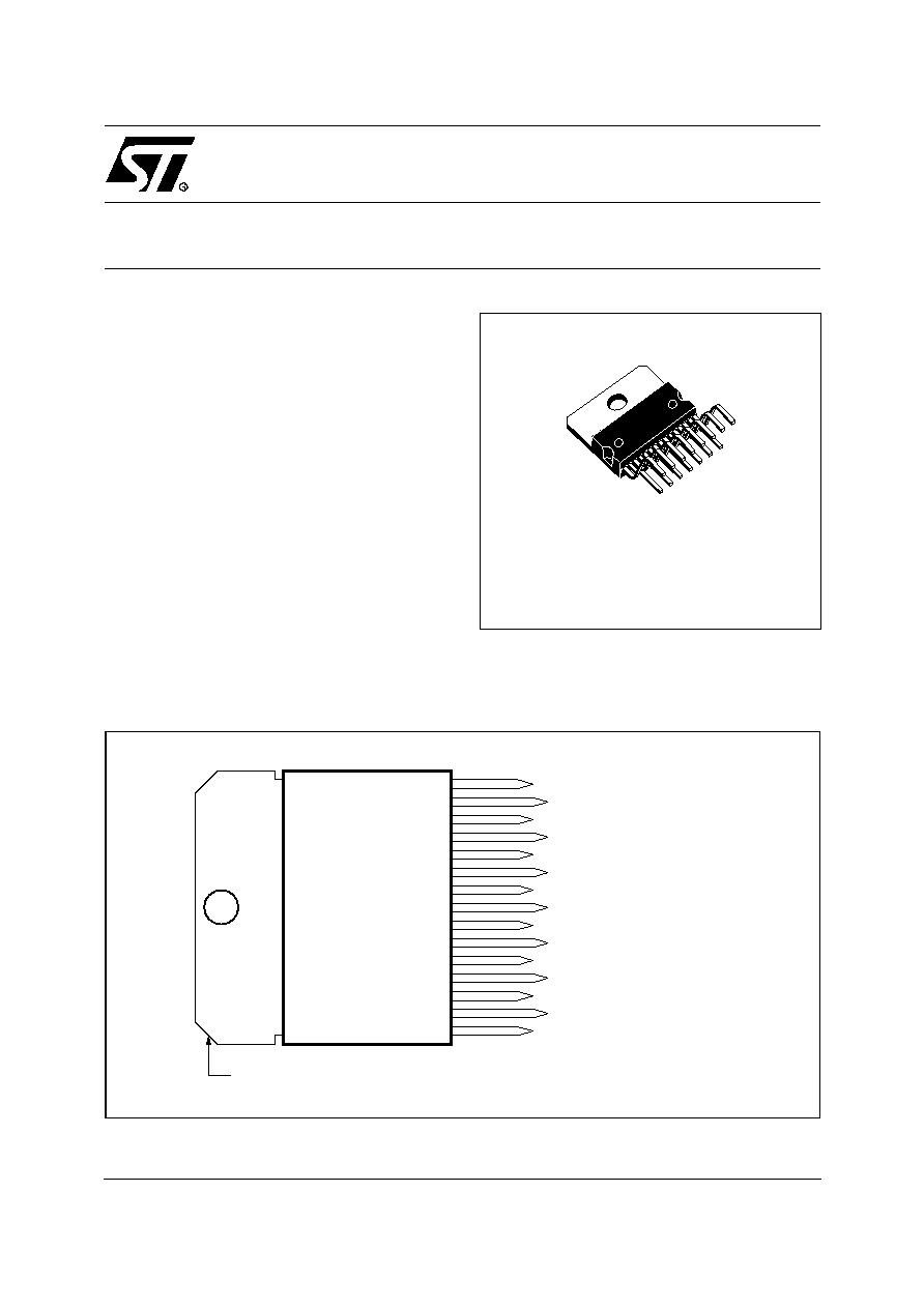
Figure 1. PIN CONNECTIONS
MULTIWATT 15
(Plastic Package)
ORDER CODE: STV5109
15
14
13
12
11
10
9
8
7
6
5
4
3
2
1
BLUE FEEDBACK
BLUE CATHODE CURRENT
BLUE OUTPUT
GREEN FEEDBACK
GREEN CATHODE CURRENT
GREEN OUTPUT
RED FEEDBACK
RED CATHODE CURRENT
RED OUTPUT
GROUND
RED INPUT
GREEN INPUT
BLUE INPUT
DD
CC
V HIGH VOLTAGE
V LOW VOLTAGE
Tab connected to Pin 8
5109-
01.eps
1
STV5109
2/7
PIN FUNCTION
N∞
Function
Description
1
Blue Input
Input of the "blue" amplifier. It is a virtual ground with 3.85V bias voltage and 75
µ
A
input bias current.
2
V
CC
Low voltage power supply, typically 12V.
3
Green Input
Input of the "green" amplifier. It is a virtual ground with 3.85V bias voltage and 75µA
input bias current.
4
Red Input
Input of the "red" amplifier. It is a virtual ground with 3.85V bias voltage and 75µA
input bias current.
5
V
DD
High voltage power supply, typically 220V.
6
Red Cathode Current
Provides the video processor with a copy of the DC current flowing into the red
cathode, for automatic cut-off or gain adjustment. If this control is not used, Pin 6
must be grounded.
7
Red Output
Output driving the red cathode. Pin 7 is internally protected against CRT arc
discharges by a diode limiting the output voltage to V
DD
.
8
Ground
Also connected to the heatsink.
9
Red Feedback
Output driving the feedback resistor network for the red amplifier.
10
Green Output
Output driving the green cathode. Pin 10 is internally protected against CRT arc
discharges by a diode limiting the output voltage to V
DD
.
11
Green Cathode Current Provides the video processor with a copy of the DC current flowing into the green
cathode, for automatic cut-off or gain adjustment. If this control is not used, Pin 11
must be grounded.
12
Green Feedback
Output driving the feedback resistor network for the green amplifier.
13
Blue Output
Output driving the blue cathode. Pin 13 is internally protected against CRT arc
discharges by a diode limiting the output voltage to V
DD
.
14
Blue Cathode Current
Provides the video processor with a copy of the DC current flowing into the blue
cathode, for automatic cut-off or gain adjustment. If this control is not used, Pin 14
must be grounded.
15
Blue Feedback
Output driving the feedback resistor network for the blue amplifier.
1
STV5109
3/7
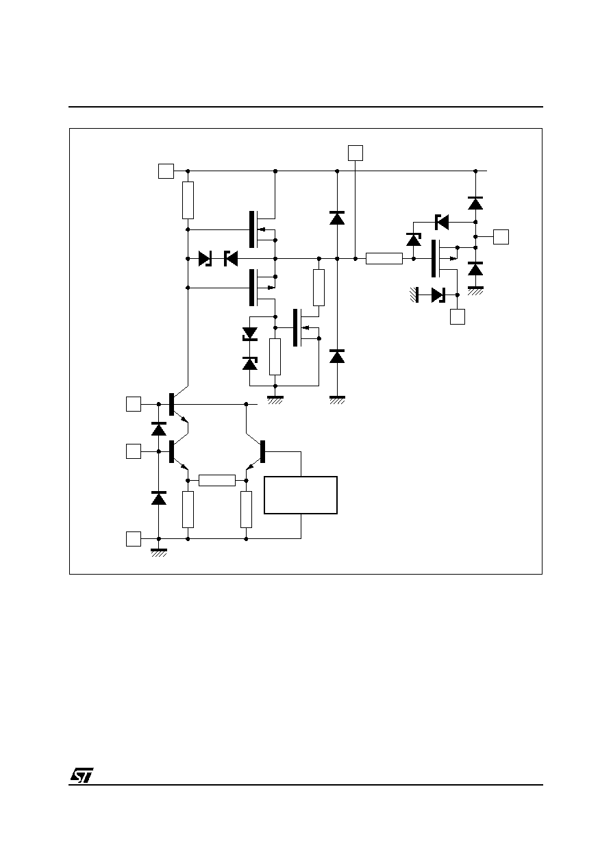
Figure 2. BLOCK DIAGRAM OF EACH CHANNEL
510
9-
02.
eps
1
2
8
REFERENCE
VOLTAGE
GND
(3, 4)
5
13
15
14
(11, 6)
(10, 7)
(12, 9)
1
STV5109
4/7
ABSOLUTE MAXIMUM RATINGS
THERMAL DATA
ELECTRICAL CHARACTERISTICS (
V
CC
= 12V ; V
DD
= 210V ; T
amb
= 25
oC
; AV = 55 unless otherwise specified)
Symbol
Parameter
Value
Unit
V
DD
Supply High Voltage
Pin 5
250
V
V
CC
Supply Low Voltage
Pin 2
20
V
I
OD
I
OG
Output Current
to V
DD
to Ground
Pins 7 - 10 - 13
Protected
8
mA
I
FD
I
FG
Output Current < 50µs duration
to V
DD
to Ground
Pins 9 - 12 - 15
45
45
mA
mA
I
j
Input Current
Pins 1 - 3 - 4
60
mA
T
j
Junction Temperature
150
∞C
T
oper
Operating Ambient Temperature
0, + 70
∞C
T
stg
Storage Temperature
- 20, + 150
∞C
Symbol
Parameter+
Value
Unit
R
th
(j-c)
Junction-Case Thermal Resistance
Max.
3
∞C/W
R
th
(j-a)
Junction-Ambient Thermal Resistance
Typ.
35
∞C/W
Symbol
Parameter
Test Conditions
Min. Typ. Max. Unit
V
DD
High Supply Voltage (Pin5)
220 240
V
V
CC
Low Supply Voltage (Pin 2)
10
12
15
V
I
DD
High Voltage Supply Internal DC Current
(without current due to the feedback network)
V
OUT
= 120V
9.5
15
mA
I
CC
Low Voltage Supply Internal DC Current
38
55
mA
V
sath
Output Saturation Voltage (High level)
(Pins7-10-13)
I
O
= - 10µA
5
V
R
ON
Output Mos Transistor (Low level)
(Pins7-10-13)
1.7
k
BW
Bandwidth at - 3dB
Measured on CRT cathodes.
(C
LOAD
= 10pF, R
PROTECT
= 1k
V
OUT
= 120V, D V
OUT
= 100V
PP
)
8
MHz
t
R
, t
F
Rise & Fall Time
Measured between 10% & 90% of
output pulse
(C
LOAD
= 10pF, R
PROTECT
= 1k
V
OUT
= 120V, D V
OUT
= 100V
PP
50
ns
G
O
Open Loop Gain
47
50
dB
Open Loop Gain Difference between
2channels
-1.5
0
1.5
dB
Open Loop Gain Temperature Coefficient
0
dB/
o
C
P
Internal Power Dissipation
(seecalculationbelow)
V
OUT
= 2MHz, 70V
PP
sine wave,
V
BLACK
= 170V, C
L
= 20pF
R
F
= 68k
3.6
dB/∞C
V
REF
Internal Voltage Reference (Pins 1-3-4)
V
OUT
= 120V
3.55 3.85 4.15
V
Voltage Reference Temperature Coefficient
0
mV/∞C
I
IB
Input Bias Current (Pins 1-3-4)
V
OUT
= 120V
75
µ
A
R
I
Input Resistance
4
k
ESD
ESD Human Body Model
1.2
kV
1
STV5109
5/7
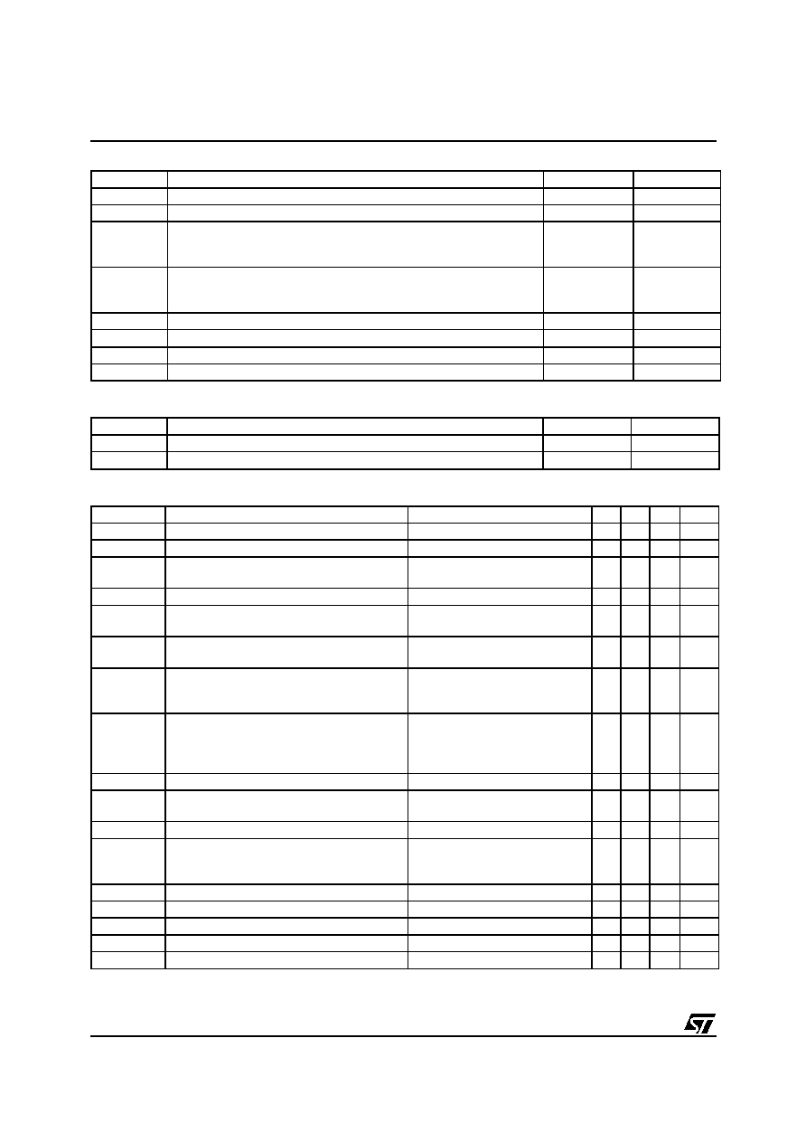
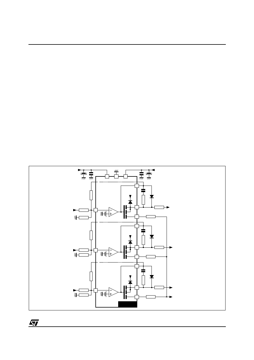
TYPICAL APPLICATION
The STV5109 is composed of three independent
amplifiers, each of them including :
≠ A differential amplifier, the gain of which is fixed
by external feedback resistors,
≠ A voltage reference,
≠ A PMOS transistor providing a copy of the cath-
ode current,
≠ A protection diode against CRT arc discharges.
PC Board Layout
The best performances of the high voltage video
amplifier will be obtained only with a carefully desi-
gned PC board. Output to input capacitance is of
particular importance.
For a single amplifier, the input-output capaci-
tance, in parallel with the relatively high feedback
resis-tance, creates a pole in the closed-loop
transfer function.
A low parasitic capacitance (0.3pF) feedback re-
sistor and HF isolated printed wires are necessary.
Furthermore, capacitive coupling from the output
of an amplifier toward the input of another one may
induce excessive cross-talk.
Power Dissipation
The power dissipation consists of a static part and
a dynamic part. The static dissipation is a function
of V
OUT
(DC), V
DD
and R
F
. Reasonable approxi-
mation of the static power can be calculated by the
following equation:
The dynamic dissipation depends on the signal
spectrum, V
OUT
, V
DD
and the load capacitance.
For a sine wave, dynamic dissipation is
P
d
= 3 x F x C
L
x V
OPP
x 0.8 x V
DD
.
The load capacitance C
L
includes CRT and board
capacitance (10pF), and amplifier output capaci-
tance (8pF) : total C
L
value is about 20pF.
Figure 3. Application Example
Ps
3 V
DD
V
DD
V
OUT
≠
(
)
40 K
-----------------------------------------------
3 V
OUT
V
DD
V
OUT
≠
(
)
R
F
--------------------------------------------------
+
=
5109-
03.eps
2
V
REF
CATHODE 1
470
W
1k
W
68k
W
4.7k
W
V
CC
12V
100nF
100
m
F
100nF
V
DD
220V
10
m
F
1.2k
W
470pF
V
DD
8
5
9
7
6
4
1.8k
W
STV5109
CATHODE 2
V
DD
12
10
11
3
CATHODE 3
V
DD
15
13
14
1
CUT-OFF
SAMPLING
1
STV5109
6/7
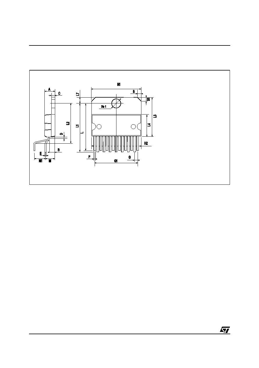
PACKAGE MECHANICAL DATA
15 PINS - PLASTIC MULTIWATT
Figure 4. 15-Pin Package
1

STV5109
7/7
Information furnished is believed to be accurate and reliable. However, STMicroelectronics assumes no responsibility for the consequences
of use of such information nor for any infringement of patents or other rights of third parties which may result from its use. No license is granted
by implication or otherwise under any patent or patent rights of STMicroelectronics. Specifications mentioned in this publication are subject
to change without notice. This publication supersedes and replaces all information previously supplied. STMicroelectronics products are not
authorized for use as critical components in life support devices or systems without the express written approval of STMicroelectronics.
The ST logo is a registered trademark of STMicroelectronics
©
2003 STMicroelectronics - All Rights Reserved.
Purchase of I
2
C Components by STMicroelectronics conveys a license under the Philips I
2
C Patent. Rights to use these components in an
I
2
C system is granted provided that the system conforms to the I
2
C Standard Specification as defined by Philips.
STMicroelectronics Group of Companies
Australia - Brazil - China - Finland - France - Germany - Hong Kong - India - Italy - Japan - Malaysia - Malta - Morocco - Singapore - Spain
Sweden - Switzerland - United Kingdom - U.S.A.
http://www.st.com