 | –≠–ª–µ–∫—Ç—Ä–æ–Ω–Ω—ã–π –∫–æ–º–ø–æ–Ω–µ–Ω—Ç: STV5345T | –°–∫–∞—á–∞—Ç—å:  PDF PDF  ZIP ZIP |
STV5345
STV5345/H - STV5345/T
TELETEXT DECODER WITH 8 INTEGRATED PAGES
April 1994
.
COMPLETE TELETEXT DECODER INCLUD-
ING ON-CHIP 8 PAGES MEMORY, REDUC-
ING EMC RADIATIONS
.
UPWARD
SOFTWARE AND HARDWARE
COMPATIBLE WITH PREVIOUS SGS-THOM-
SON's DECODER SDA5243
.
DIRECT INTERFACE TO AN EXTERNAL
STATIC RAM OF 8kBYTES FOR UP TO 16
PAGES APPLICATION
.
AUTOMATIC SELECTION OF UP TO SIX NA-
TIONAL LANGUAGES
.
FOUR SIMULTANEOUS PAGE REQUESTS
.
DISPLAY OF THE 25TH STATUS ROW
.
MICROPROCESSOR CONTROL VIA AN I
2
C
BUS (SLAVE ADDRESS 0010001 R/W)
.
DATA
ACQUISITION
AVAILABLE
FROM
LINES 2 TO 22 OR FROM A COMPLETE
FIELD
.
HIGH QUALITY DISPLAY USING A CHARAC-
TER MATRIX OF 12 x 10 DOTS
.
SINGLE + 5V SUPPLY VOLTAGE
.
ON-CHIP
MASK PROGRAMMABLE ROM
CHARACTER GENERATORS
.
HCMOS PROCESS
1
2
3
4
5
6
7
8
9
10
11
12
40
39
38
37
36
35
34
33
32
31
30
29
28
27
26
25
13
14
15
16
17
18
19
20
24
23
22
21
A11
A12
OE
WE
TTD
TTC
ODD/EVEN
F6
SAN D
TCS/SCS
R
G
B
COR
B LA N
Y
SCL
SDA
V
D D
A10
A9
A8
A7
A6
A5
A4
A3
A2
A1
A0
D7
D6
D5
D4
D3
D2
D1
D0
V
SS
VCS
5345-01.EPS
PIN CONNECTIONS
DESCRIPTION
The STV5345 is a HCMOS integrated circuit which
performs all the processing of logical data within a
625 lines system teletext decoder. It is designed to
operate in conjunction with one-chip : the SAA5231
integrated chip which extracts Teletext information
embedded in a composite video signal. Up to 8
pages of display data can be stored in internal
memory. Using 8Kbytes of external memory leads
to a 16 pages application. A complete system also
comprises a microprocessor controlling the
STV5345 via a 2-wires serial bus. An on-chip ROM
memory contains the character sets. The STV5345
performs automatic selection of one of up to six
natural languages. Data bytes may be decoded in
either 7-Bit plus parity or in full 8-Bit formats. The
chip set also supports facilities for reception and
display of higher-level protocol data.
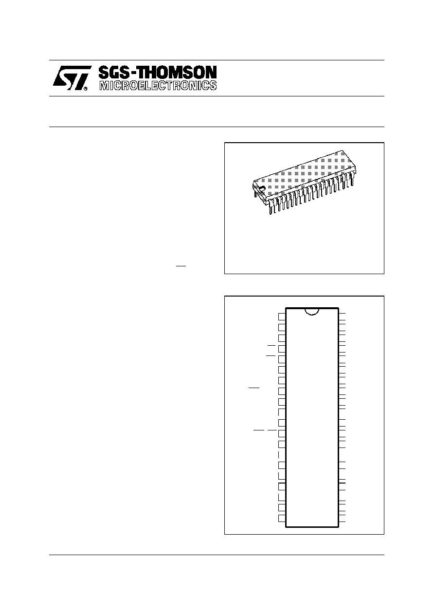
DIP40
(Plastic Package)
ORDER CODE : STV5345
West European
STV5345/H
East European
STV5345/T
Turkish & European
1/25
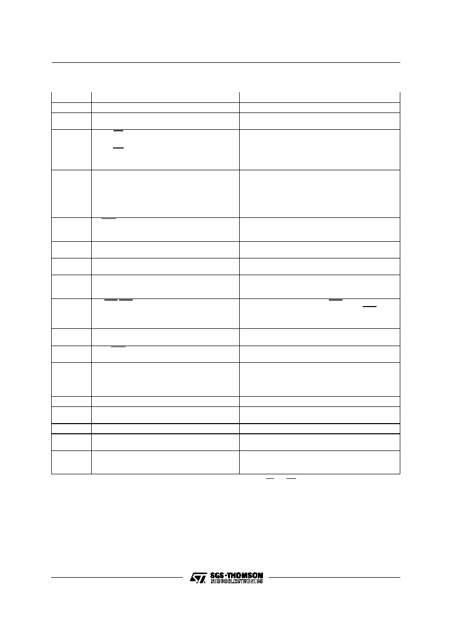
PIN DESCRIPTION
Pin
Symbol
Function
Description
1
V
DD
+5V
Positive supply voltage
2,3,40 *
A11, A12, A10
Chapter address
Address selection outputs for 1 of 8 external static
RAM chapters each of 1 kBytes.
4 *
OE
Output enable
Active-low external static RAM output enable control
signal.
5 *
WE
Write enable
Active-low external static RAM write enable control
signal. It supports write-cycles interleaved with
read-cycles.
6
TTD
Teletext data input
An A.C. coupled teletext data input supplied by the
SAA5231 chip is latched to V
SS
between 4 and 8
µ
s
after each TV line.
7
TTC
Teletext clock input
A 6.9375MHz clock signal, supplied by the SAA5231
chip, is internally A.C. coupled, clamped and
buffered.
8
ODD/EVEN
Interlaced mode state output
High for even numbered and low for odd-numbered
frames. The value is valid 2
µ
s before the end of
lines 311 and 624.
9
F6
Character display clock signal
The 6MHz clock signal, supplied by the SAA5231
chip is internally A.C. coupled, clamped and buffered.
10
VCS
Video composite
synchronization input signal
Active high VCS input.
11
SAND
Sandcastle
Three level output pulse to the SAA5231 device.
Phase lock, blanking signal, and color burst
components are contained in this signal.
12
TCS/SCS
Input / output composite
synchronization signal
Scan composite input signal (SCS) for the display
synchronization or Text composite sync. (TCS)
output signal to the SAA5231. Both signals are
active low.
13,14,15
R G B
Red, green, blue
Character and background colors active-high
open-drain outputs.
16
COR
Contrast reduction
Open-drain active-low output supporting optimal
display of characters in "mixed mode" operation.
17
BLAN
Blanking signal output
Open-drain active high output for TV-image blanking
in normal and mixed-mode operation.
18
Y
Foreground output
Open-drain active-high output with foreground
information. Can be used for printer command.
19
SCL
Serial clock
Microprocessor clock input via serial bus.
20
SDA
Serial data input / output
Open-drain microprocessor serial data input/output
via serial bus.
21
V
SS
0 Volt
Ground.
22-29 *
D0-D7
Parallel data input / output
Eight tri-state input/output for data read/write from/to
an external static RAM.
30-39 *
A0-A9
Address signals
Ten addresses output pins for accessing to
individual Bytes of a 1 kByte chapter stored in an
external Static RAM.
5345-01.TBL
* Pins only activated when 8KBytes of external memory are addressed, otherwise pins OE and WE remain high, and others remain low.
STV5345 - STV5345/H - STV5345/T
2/25
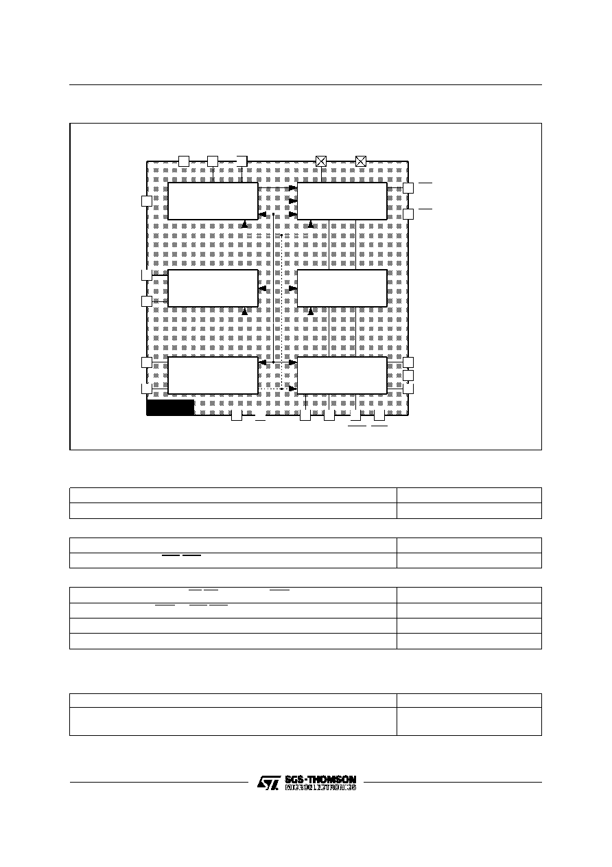
12
18
17
16
8
13
15
14
DATA
ADDRESS
CTRL
ADDRESS
CTRL
DATA
4
5
19
20
7
6
9
11
10
DATA
CLOC K
OE
WE
RED
GREEN
BLUE
SCL
SDA
TTC
TTD
F6
VCS
SAND
TCS/
SCS
A0 .. . A12
D0 .. . D7
*
*
*
A0 ... A10 / 30 ... 40
A11 - A12 / 2 - 3
D0 ... D7 / 22 .. . 29
*
V
DD
V
SS
1
21
Y
BLAN
COR ODD/
EVEN
EXTERNAL
MEMORY
INTERFACE
TIME BASE
DATA ACQUISITION
&
DATA PROCESSING
8 PAGES
INTERNAL
MEMORY
DISPLAY &
CONTROL
INTERFACE
I C BUS
INTERFACE
2
STV5345
5345-02.EPS
BLOCK DIAGRAM
ABSOLUTE MAXIMUM RATINGS
Symbol
Parameter
Value
Unit
V
DD
Power Supply Range
-0.3, +6.0
V
INPUT VOLTAGE RANGE :
V
I
VCS,SDA,SCL,D0-D7
-0.3, V
DD
+ 0.5
V
V
I
TTD,F 6,TCS/SCS,TT C
-0.3, +10
V
OUTPUT VOLTAGE RANGE :
V
O
SAND,A0-A12,OE,WE,D0-D7,SDA,ODD/E VEN,R,G,B
-0.3 , V
DD
V
V
O
BLAN,COR, Y, TCS/SCS
-0.3 , V
DD
V
T
stg
Storage Temperature Range
-20, +125
o
C
T
A
Operating Ambient Temperature Range
-20, +70
o
C
5345-02.TBL
ELECTRICAL CHARACTERISTICS
V
DD
= 5V, V
SS
= 0V, T
A
= - 20 to + 70
o
C
Symbol
Parameter
Min
Typ
Max
Unit
V
DD
Supply Voltage (Pin 1)
4.5
5
5.5
V
I
DD
Supply Current (operating mode)
15
40
mA
5345-03.TBL
STV5345 - STV5345/H - STV5345/T
3/25
ELECTRICAL CHARACTERISTICS (continued)
V
DD
= 5V, V
SS
= 0V, T
A
= - 20 to + 70
o
C
Symbol
Parameter
Min
Typ
Max
Unit
INPUTS
TTD (Pin 6)
C
EXT
Ext. Coupling Capacitor
50
nF
V
I(p-p)
Input Voltage p-p
2
7
V
t
r
, t
f
Input Rise / Fall Times
10
80
ns
t
DS
Input Set-up Time
40
ns
t
DH
Input Hold Time
40
ns
I
I(L)
Input Leakage Current (V
I
= 0 to V
DD
)
-10
+10
µ
A
C
I
Input capacitance
7
pF
TTC, F6 (Pins 7,9)
V
I
DC Input Voltage
- 0.3
+10
V
V
I(p-p)
AC Input Voltage F6
AC Input Voltage TTC
1
1.5
7
7
V
V
±
V
P
Input Peak Rel. 50 % Duty
0.2
3.5
V
f
TTC
TTC Clock Frequency
6.9375
MHz
f
F6
F6 Clock Frequency
6
MHz
t
r
, t
f
Clock Rise / Fall Times
10
80
ns
I
I(L)
Input Leakage Current (V
I
= 0 to 10V)
-10
+10
µ
A
C
I
Input Capacitance
10
pF
VCS (Pin 10)
V
IL
Low Level Input Voltage
0
0.8
V
V
IH
High Level Input Voltage
2
V
DD
V
t
r
, t
f
Input Rise / Fall Times
500
ns
I
I(L)
Input Leakage Current (V
I
= 0 to V
DD
)
-10
+10
µ
A
C
I
Input Capacitance
7
pF
SCL (Pin 19)
V
IL
Low Level Input Voltage
0
1.5
V
V
IH
High Level Input Voltage
3
V
DD
V
f
SCL
SCL Clock Frequency
100
kHz
t
r
, t
f
Input Rise / Fall Times
2
µ
s
I
I(L)
Input Leakage Current (V
I
= 0 to V
DD
)
-10
+10
µ
A
C
I
Input Capacitance
7
pF
INPUT/OUT PUTS
TCS(output), SCS(input) (Pin12)
V
IL
Low Level Input Voltage
0
1.5
V
V
IH
High Level Input Voltage
3
8
V
t
r
, t
f
Input Rise / Fall Times
500
ns
I
I(L)
Input Leakage Current
(V
I
= 0 to V
DD
and output in high impedance state)
-10
+10
µ
A
C
I
Input Capacitance
7
pF
V
OL
Low Level Output Voltage (I
OL
= 0.4mA)
0
0.4
V
V
OH
High Level Output Voltage (-I
OH
= 0.2mA)
2.4
V
DD
V
t
r
, t
f
Output Rise / Fall Times between 0.6V and 2.2V
100
ns
C
L
Load Capacitance
50
pF
5345-04.TBL
STV5345 - STV5345/H - STV5345/T
4/25
ELECTRICAL CHARACTERISTICS (continued)
V
DD
= 5V, V
SS
= 0V, T
A
= - 20 to + 70
o
C
Symbol
Parameter
Min
Typ
Max
Unit
INPUT/OUT PUTS (continued)
SDA (Pin 20)
V
IL
Low Level Input Voltage
0
1.5
V
V
IH
High Level Input Voltage
3
V
DD
V
t
r ,
t
f
Input Rise / Fall Times
2
µ
s
I
I(L)
Input Leakage Current (V
I
= 0 to V
DD
and output in high impedance state)
-10
+10
µ
A
C
I
Input Capacitance
7
pF
V
OL
Low Level Output Voltage (I
OL
= 3mA)
0
0.5
V
t
f
Output Fall Time between 3.0V and 1.0V
200
ns
C
L
Load Capacitance
400
pF
D0-D7 (Pins 22-29)
V
IL
Low Level Input Voltage
0
0.8
V
V
IH
High Level Input Voltage
2
V
DD
V
I
I(L)
Input Leakage Current (V
I
= 0 to V
DD
and output in high impedance state)
-10
+10
µ
A
C
I
Input Capacitance
7
pF
V
OL
Low Level Output Voltage (I
OL
= 1.6mA)
0
0.4
V
V
OH
High Level Output Voltage (-I
OH
= 0.2mA)
2.4
V
DD
V
t
r ,
t
f
Output Rise / Fall Times between 0.6V and 2.2V
50
ns
C
L
Load Capacitance
120
pF
OUTPUTS
A0-A12, OE, WE (Pins 30-40,2,3,4,5,)
V
OL
Low Level Output Voltage (I
OL
= 1.6mA)
0
0.4
V
V
OH
High Level Output Voltage (-I
OH
= 0.2mA)
2.4
V
DD
V
t
r
, t
f
Output Rise / Fall Times between 0.6V and 2.2V
50
ns
C
L
Load Capacitance
120
pF
ODD/EVEN (Pin 8)
V
OL
Low Level Output Voltage (I
OL
= 0.4mA)
0
0.4
V
V
OH
High Level Output Voltage (-I
OH
= 0.2mA)
2.4
V
DD
V
t
r
, t
f
Output Rise / Fall Times between 0.6V and 2.2V
100
ns
C
L
Load Capacitance
50
pF
SAND (Pin 11)
V
OL
Low Level Output Voltage (I
OL
= 0.2mA)
0
-
0.25
V
V
OI
Middle Level Output Voltage (I
OL
=
±
10
µ
A)
1.1
-
2.9
V
V
OH
High Level Output Voltage (-I
OH
= 0 to 10
µ
A)
4
V
DD
V
t
r1
t
r2
Output Rise Time :
l
V
OL
to V
OI
from 0.4 to 1.1V
l
V
OI
to V
OH
from 2.9 to 4.0V
-
-
-
-
400
200
ns
t
f
Output Fall Time V
OH
to V
Ol
from 4.0 to 0.4V
-
-
50
ns
C
L
Load Capacitance
-
-
30
pF
5345-05.TBL
STV5345 - STV5345/H - STV5345/T
5/25