 | –≠–ª–µ–∫—Ç—Ä–æ–Ω–Ω—ã–π –∫–æ–º–ø–æ–Ω–µ–Ω—Ç: STV5715 | –°–∫–∞—á–∞—Ç—å:  PDF PDF  ZIP ZIP |
STV5715
ADVANCED 2-HEAD
PLAY-BACK AND RECORD AMPLIFIER FOR VCR
November 1993
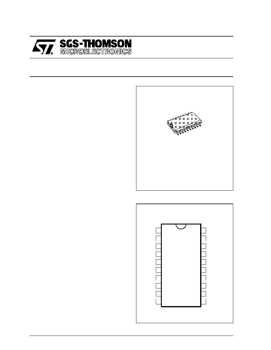
SO20 LARGE
(Plastic Micropackage)
ORDER CODE : STV5715
PLAY-BACK MODE
.
LOW NOISE AND WIDE BAND AMPLIFIERS
FOR 2 HEADS
.
AUTOMATIC OFFSET CANCELLATION BE-
TWEEN THE 2 SELECTED HEADS
.
ONE PLAY-BACK OUTPUT WITHOUT AGC
.
ONE PLAY-BACK OUTPUT INCLUDING AGC
.
RECORD AMPLIFIER INHIBITION AND RE-
CORD OUTPUT GROUNDED
.
OUTPUT FOR TRACKING VIDEO INFORMA-
TION (TRIV) WITH ADJUSTABLE GAIN
RECORD MODE
.
ONE INTEGRATED I/I CONVERTER WITH
ACCURATE CONTROL OF TRANSCONDUC-
TANCE
.
AUTOMATIC PLAY-BACK/RECORD SWITCH-
ING BY SCANNING OF RECORD SUPPLY
.
PLAY-BACK LOOP INHIBITION
1
2
3
4
5
6
7
8
9
10
20
19
18
17
16
15
14
13
12
11
GND1
CCAS
H1
GND2
H2
C2
C1
CAGC
GND3
TRIVADJ
V
MES
SW M
SW H
CHROMA
V
IN
LUMA
V
CC
TRIV
REC
V
OUT
I
5715-01.EPS
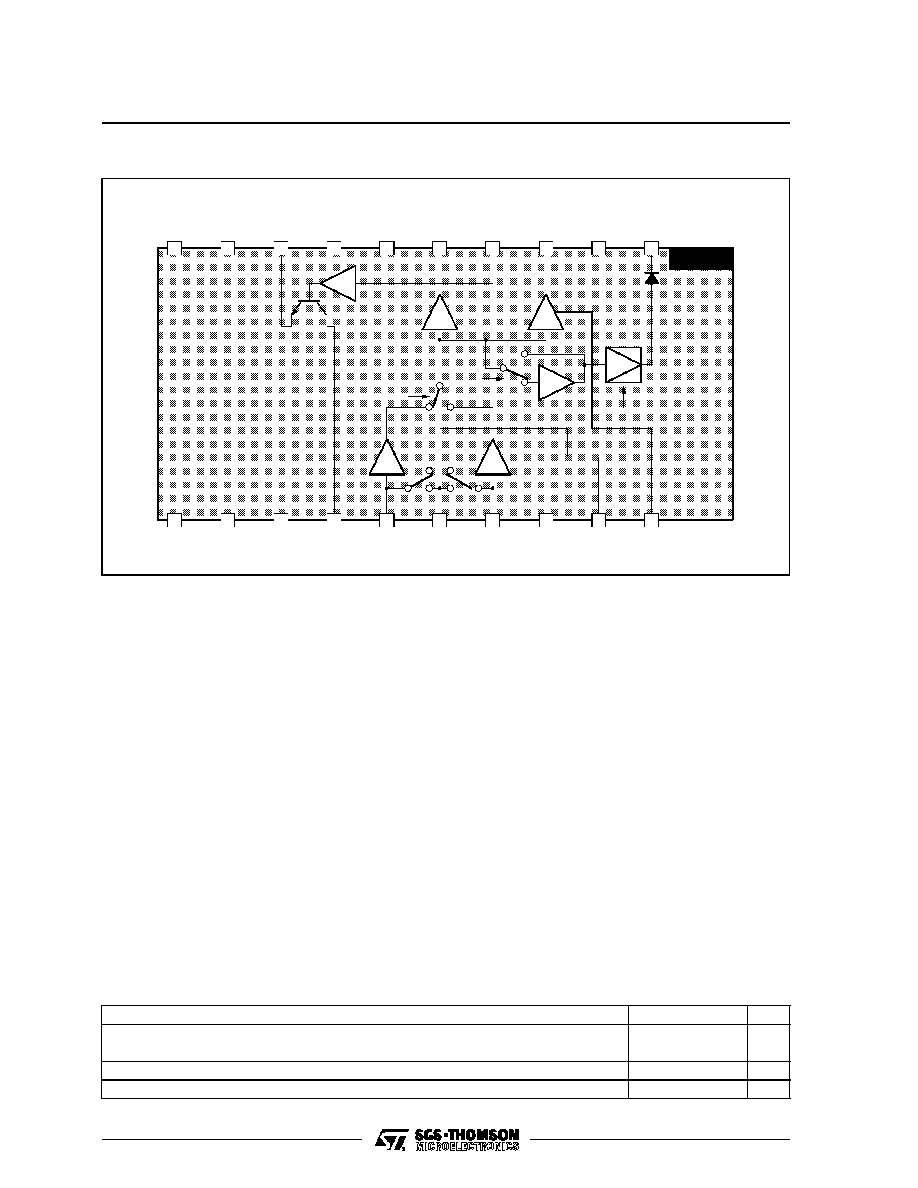
PIN DESCRIPTION
DESCRIPTION
The STV5715 is an advanced two head record and
play-back amplifier for VCR.
1/9
11
12
13
14
15
16
17
18
19
20
TRIVADJ
LSP
SW H
SW M
HLP
1
2
3
4
5
6
7
8
10
H
L
GND3
TRIVADJ
V
MES
SW
M
SW
H
CHROMA
V
IN
LUMA
V
CC
TRIV
G
ND1
CCAS
H1
GND2
H2
C2
C1
CAGC
V
REC
I
OUT
9
STV5715
5715-02.EPS
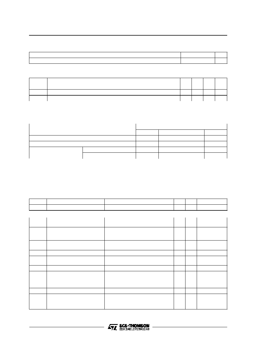
BLOCK DIAGRAM
FUNCTIONAL DESCRIPTION
STV5715 is intended for 2 heads VCR applications.
It includes all the electrical functions necessary to
achieve play-back and record processing for VHS
and S-VHS applications (10MHz bandwidth).
High performancetechnologyallows very low noise
levels (current and voltage), which are frequency
independant in all the frequency range. In play-
back mode a special feature suppresses the DC
offset when switching the two channels. Optimized
play-back output stage gives to the STV5715 large
capability to drive directly a coaxial cable in order
to reduce number of external components.
Two play-back outputs are availabe : one, dedi-
cated to Chroma processing, is a 60dB voltage
amplifier output, the other, dedicatedto Luma proc-
essing, is phase opposite signal with a constant AC
output level of 200mV
PP
at 3.8MHz signal.
A tracking information for video signal (TRIV) is
Luma amplitude proportional and allows automatic
phase correction. The transfer function has a gain
of 2.5dB higher when a LP channel is selected.
Adding to this, a gain control bloc allows to modify
the gain (
±
6dB) of the TRIV function for all the
channels by applying a bias on pin TRIVADJ.
An automatic scanning of record supply voltage
permits STV5715 automatically switching either in
play-back or in record mode. The switching thresh-
old voltage is fixed to a value which forbids high
current peaking through the heads.
During play-back mode, record output is grounded
via an internal transistor and during record mode
preamplifiers are turned off.
There is one output current for two recording
heads, the DC current and the AC characteristics
can be very precisely controlled with accurate ex-
ternal resistors. If recommended resistances are
used, a
±
3% transconductanceaccuracy is guar-
anteed.
STV5715 is fully protected against ESD.
ABSOLUTE MAXIMUM RATINGS
Symbol
Parameter
Value
Unit
V
CC
Power Supply Voltage
6
V
V
REC
Power Supply Voltage Record
15
V
T
J
Junction Temperature
+150
o
C
T
oper
Operating Temperature
0, +70
o
C
5715-01.TBL
STV5715
2/9
THERMAL DATA
Symbol
Parameter
Value
Unit
R
th (j-a)
Junction-ambient Thermal Resistance
Typ.
70
o
C/W
5715-02.TBL
RECOMMENDED OPERATING CONDITIONS (T
amb
= 25
o
C)
Symbol
Parameter
Min.
Typ.
Max.
Unit
V
CC
Power Supply Voltage
4.5
5
5.5
V
V
REC
Power Supply Voltage Record
4.75
11.3
12.6
V
CAGC
Capacitance at Pin CAGC
4.7
nF
5715-03.TBL
ELECTRICAL OPERATING CHARACTERISTICS (T
amb
= 25
o
C unless otherwise specified)
Power Consumption
Parameter
Play-Back
Record (1)
Typ.
Max.
Typ.
Max.
V
CC
42mA
52mA
25mA
38mA
V
REC
0mA
0mA
25mA
33mA
Total
Consumption (2)
V
CC
= 5V, V
REC
= 9V
210mW
350mW
V
CC
= 5.5V, V
REC
= 9.45V
286mW
521mW
Notes : 1.
R1 = 18
2.
Taking in account only the consumption through the IC.
A great care should be taken to the maximum power consumption : V
REC
can be increased to 12.6V if the DC current flowing
through the head is reduced. This can be done by increasing R1 value. V
REC
can be reduced as long as voltage on Pin
I
OUT
does not fall below 1V (to avoid output stage saturation).
5715-04.TBL
Play-back Mode
V
CC
= 5V, no load on Pins CHROMA,LUMA
Symbol
Parameter
Test Conditions
Min.
Typ. Max.
Unit
I
CC1
Supply Current
32
42
52
mA
CHROMA OUTPUT (no AGC)
G
PB
Pre-amplification Gain
Sinewave 600 kHz, 400mV
PP
on output
Input on Pin H1 or H2
56
59
62
dB
G
PB1
Difference of Output Signal on
Pin CHROMA between Channel
1 and Channel 2
Sinewave 600kHz
0.4mV
PP
on inputs H1 and H2
-1.2
0
1.2
dB
e
N
Equivalent Input Voltage Noise
Level
Input grounded via switching transistor
on Pins H1, H2, f = 600kHz
0.6
nV
/
Hz
i
N
Equivalent Input Current Noise
Pins H1, H2
1.7
pA
/
Hz
CRT
Crosstalk
Sinewave 3.8MHz, 400
µ
V
PP
on input,
All the other inputs loaded with R
g
= 15
-45
-40
dB
R
PB
Playback Switch-on Resistance
I = 10mA
2.0
5.0
F
LCPB1
F
HCPB1
Bandwidth Cut-off Frequency
-3dB attenuation 50
in parallel on the
input, 0dB at 600kHz
Low
High
8
13.5
0.1
MHz
MHz
C
IN
Input Capacitance Pins H1, H2
At 5MHz
30
40
pF
R
IN
Pre-amplifier Input Resistance
Pins H1, H2
At 3.8MHz
400
600
900
Z
CPB
Output ImpedancePin CHROMA
DC
24
50
5715-05.TBL
STV5715
3/9
ELECTRICAL OPERATING CHARACTERISTICS (T
amb
= 25
o
C unless otherwise specified) (continued)
Play-back Mode
V
CC
= 5V, no load on Pins CHROMA,LUMA
Symbol
Parameter
Test Conditions
Min.
Typ. Max.
Unit
CHROMA OUTPUT (no AGC) (continued)
V
DCPB1
DC Level at Play-back Output
on Pin CHROMA
1.5
1.9
2.3
V
V
DC
Head Switch Offset Pin CHROMA
-100
0
100
mV
SH
PB1
Second Harmonic Play-back Output
Pin CHROMA
Sinewave 3.8MHz
400
µ
V
PP
on input
-45
-40
dB
LUMA OUTPUT (with AGC)
Z
LPB
Output Impedance
DC
30
50
V
DCPB2
DC Level
1.1
1.5
2.1
V
F
LCPB2
F
HCPB2
Bandwidth Cut-off Frequency
-3dB attenuation 50
in parallel on the
input, AGC locked, 0dB at 3.8MHz
Low
High
10
12.5
0.1
MHz
MHz
V
LPB
Output Amplitude
Input signal 200
µ
V
PP
at 3.8MHz on Pins
H1, H2
140
200
270
mV
PP
V
LPB
AGC Control Sensitivity
Input signal 200
µ
V
PP
at +6dB or -5dB on
Pins H1, H2
-2
+1
dB
SH
PB2
Second Harmonic Play-back Output
Input Signal 3.8MHz 400
µ
V
PP
on Pins
H1, H2
-44
-39
dB
CAGC
I+
Positive Output Current
Input Signal 3.8MHz 200
µ
V
PP
on H1
15
30
50
µ
A
I-
Negative Output Current
Input Signal 3.8MHz 200
µ
V
PP
on H1
-50
-30
-15
µ
A
TRIV
I
TRIV
Downloading Current
200
300
400
µ
A
V
TRIV1
Output Level (1)
With no signal, V
TRIVADJ
= 2.5V
Mode LP (SW-M = high)
0.3
0.6
1.5
V
V
TRIV2
Output Level (2)
V
CHROMA
= 100mV
PP
at 4MHz
V
TRIVADJ
= 2.5V, Mode LP (SW-M = high)
1.91
2.31
2.91
V
V
TRIV3
Output Level (3)
V
CHROMA
= 400mV
PP
at 4MHz
V
TRIVADJ
= 2.5V, Mode LP (SW-M = high)
3.525 3.725 3.985
V
V
TRIV4
Output Level (4)
V
CHROMA
= 100mV
PP
at 4MHz
V
TRIVADJ
= 1V, Mode LP (SW-M = high)
1.110 1.610 2.311
V
V
TRIV5
Output Level (5)
V
CHROMA
= 100mV
PP
at 4MHz
V
TRIVADJ
= 4V, Mode LP (SW-M = high)
2.875 3.075 3.335
V
V
TRIV6
Output Level (6)
V
CHROMA
= 400mV
PP
at 4MHz
V
TRIVADJ
= 2.5V, Mode SP (SW-M = low)
3.215 3.415 3.675
V
V
TRIV7
Output Level (7)
V
CHROMA
= 100mV
PP
at 4MHz
V
TRIVADJ
= 2.5V, Mode SP (SW-M = low)
1.65
2.05
2.65
V
f
TRIV1
Response Lower Frequency
V
CHROMA
= 400mV
PP
at 4MHz and 1MHz
V
TRIVADJ
= 2.5V, Mode LP (SW-M = high)
-10
-6
-3
dB
f
TRIV2
Response Higher Frequency
V
CHROMA
= 400mV
PP
at 8MHz and 4MHz
V
TRIVADJ
= 2.5V, Mode LP (SW-M = high)
-2.5
-1
-0
dB
G
TRIV
High Level Input
LP : V
CHROMA
= 100mV
PP
, 300mV
PP
at
4MHz, V
TRIVADJ
= 2.5V
4
5.5
7
V/V
5715-06.TBL
STV5715
4/9

ELECTRICAL OPERATING CHARACTERISTICS (T
amb
= 25
o
C unless otherwise specified) (continued)
Record Mode
V
REC
= 11.3V, V
CC
= 5V, Load resistor 50
on Pin I
OUT
Transconductance network defined by :
R1 = 18
, 1%
Pins GND/V
MES
R2 = 1.5k
, 1%
Pins V
MES
/V
IN
R3 = 1.5k
, 1%
Pin V
IN
Symbol
Parameter
Test Conditions
Min.
Typ. Max.
Unit
I
REC
I
CC2
Current Supply
V
REC
= 11.3V
V
CC
= 5V
17
15
25
25
33
38
mA
mA
I
max
Max. Record Current
3.8MHz
35
mA
PP
TR
Transconductance
V
IN
= 300mV
PP
45
55
65
mA/V
SH
REC
Second Harmonic
Output Current, 30mA
PP
at 3.8MHz
at Pin I
OUT
-54
-38
dB
F
LCR
FHCR
Bandwidth Cut-off Frequency Pin IOUT
-3dB attenuation, 0dB at 3.8MHz
Output current 30mA
PP
Low
High
10
0.1
MHz
MHz
R
VIN
Input Resistance on Pin V
IN
Equivalent value of R3 resistor
500
700
900
5715-07.TBL
Switching Levels
Symbol
Parameter
Test Conditions
Min.
Typ.
Max.
Unit
V
SWHH
Head Selection Pin SW-H
Head number 1
2.4
V
CC
V
V
SWHL
Head number 2
0
1.5
V
I
SWHH
Input current (5V)
5
15
50
µ
A
I
SWHL
Output current (0V)
-50
-20
0
µ
A
V
SWMH
Mode Selection Pin SW-M
LP Mode
2.4
5
V
V
SWML
SP mode
0
1.5
V
I
SWMH
Input current (5V)
5
15
50
µ
A
I
SWML
Output current (0V)
-50
-20
0
µ
A
t
ON
t
OFF
Selection Pin SW-H Transient
Response
Output signal appears on Pin CHROMA
Delay time selection ON
Delay time selection OFF
100
100
500
500
ns
V
TH1
Inhibition Threshold Hysteresis for
Switching from Play-back to record
on Pin V
REC
V
CC
= 5V
0.15
0.3
0.5
V
V
TH2
Inhibition Threshold Hysteresis for
Switching from Record to Play-back
on Pin V
REC
V
CC
= 5V
80
mV
t
1
Transient Response of Record
Scanning on Pin V
REC
Delay from play-back to record
(signal disappears on Pin CHROMA)
10
µ
s
t
2
Delay from record to play-back
(signal appears on Pin CHROMA)
32*
ms
t
3
Delay from play-back to record (signal
appears on Pin I
OUT
)
0.2
ms
t
4
Delay from record to play-back (signal
disappears on Pin I
OUT
)
11*
ms
* Depending on capacitance on Pin V
REC
; above values are according to the application diagram at page 9.
5715-08.TBL
STV5715
5/9