STV5730
MULTISTANDARD ON-SCREEN DISPLAY
FOR VCR, PAY-TV, SATELLITE RECEIVER
October 1994
ADVANCE DATA
SO28
(Plastic Micropackage)
ORDER CODE : STV5730
.
A CHARACTER GENERATOR WITH ASCII
RAM AND CHARACTER ROM :
- 128 characters
- 12 dots x 18 lines character composition
- 11 rows x 28 characters page composition
.
ACCURATE INTERNAL BANDGAP VOLTAGE
REFERENCE
.
LINE LOCKED PLL
.
VIDEO TIMING GENERATOR
.
INPUT CVBS CLAMP AND SYNC EXTRAC-
TOR
.
VERTICAL SYNC SEPARATOR
.
INPUT CVBS SYNC RE-INSERTION
.
INPUT CVBS PRESENCE DETECTOR
.
PAL/NTSC CHROMA ENCODER
.
DEDICATED PINS FOR LUMA AND CHROMA
EXTERNAL FILTERING
.
GAIN ON CVBS OUTPUT FOR EITHER 0dB
OR 6dB CAPABILITY
.
MULTISTANDARD
TRANSLUCENT MIXED
MODE
.
OPAQUE MIXED MODE
.
NORMAL FULL PAGE MODE
.
VIDEO FULL PAGE MODE
.
SUITABLE FOR S-VHS
.
THREE DIFFERENT MARKERS CAN BE
GENERATED SIMULTANEOUSLY
.
THREE WIRE SERIAL INTERFACE FOR MI-
CROPROCESSOR CONTROL
This is advance information on a new product now in development or undergoing evaluation. Details are subject to change without no tice.
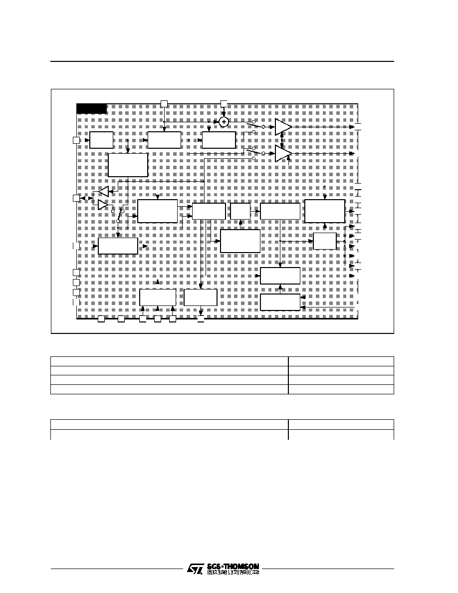
DESCRIPTION
The STV5730 IC is intended to be used in VCR,
Satellite receiver and PAY-TV systems for CVBS or
R/G/B text/graphics insertion.
1
2
3
4
5
6
7
8
9
10
11
12
13
14
28
27
26
25
24
23
22
21
20
19
18
17
16
YOUT
VIDEO IN
FTR
RES
CSYNC
MUTE
DATA
CLK
CSN
R
XTAL OUT
FB
CO
BAR
DGND
AGND
LECHAR
LESCREEN
COUT
CIN
YIN
VIDEO OUT2
15
XTAL IN
VIDEO OUT1
B
G
DV
DD
AV
DD
5730-01.EPS
PIN CONNECTIONS
1/19
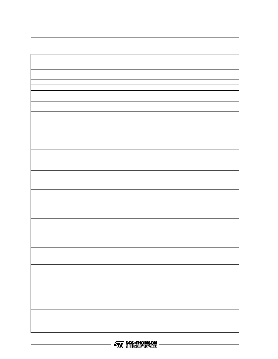
PIN DESCRIPTION
N
o
Name
Type
Description
1
YOUT
Analog Output This pin outputs the luma to allow the user to notch filter it. This pin may be
connected to the YIN input for minimum cost applications.
2
VIDEO IN
Analog Input
This is the CVBS input. An external capacitor is needed for clamp operation.
The STV5730 extracts the sync from this signal when the C7 control bit is set.
3
RES
Analog Pin
it must be tied to an external resistor to control the PLL f0 frequency.
4
FTR
Analog Pin
it must be tied to the line PLL loop filter.
5
AV
DD
Supply Pin
5V analog supply pin.
6
DV
DD
Supply Pin
5V digital supply pin.
7
CSYNC
Bidirectional
Pin
This pin inputs the mixed mode composite sync when the C7 control bit is
cleared. It outputs the video in extracted sync when the C7 control bit is set.
8
XTAL IN
Digital Input
This is the 4*fsc quartz input. The quartz may be started or stopped under
control of dedicated serial interface messages. Alternatively, a 4fsc clock can
be input directly. The stop message must not be used in this case.
9
XTAL OUT
Digital Output
This is the 4*fsc quartz output. The quartz may be started or stopped under
control of dedicated serial interface messages.
10
MUTE
Digital Output
This pin indicates if the CVBS input signal is present on VIDEO IN input pin.
It is forced low if the M2 mode bit is cleared.
11
DATA
Digital Input
This is the serial interface data input.
12
CLK
Digital Input
This is the serial interface clock input.
13
CSN
Digital Input
This is the serial interface chip select input.
14
R
Digital Output
This is the Red signal output. It is forced low during the horizontal and vertical
blanking intervals.
15
G
Digital Output
This is the Green signal output. It is forced low during the horizontal and
vertical blanking intervals.
16
B
Digital Output
This is the Blue signal output. It is forced low during the horizontal and vertical
blanking intervals.
17
FB
Digital Output
This is the fast blanking output. It is delivered to control an external R/G/B
switch for R/G/B or TV applications.
18
CO
Digital Output
This is the character activity output. It indicates if a character foreground is
being displayed, and can be used to control its intensity.
19
BAR
Digital Input
This input forces the PLL in free run mode when active. It is enabled if the M0
mode bit is set.
20
DGND
Supply Pin
0V digital ground.
21
AGND
Supply Pin
0V analog ground.
22
LECHAR
Analog Input
This pin determines the character intensity level in external bias mode (ie
when the C10 control bit is set). This level must be defined relative to the
internal black reference. A variable luminance signal may be entered. To be
grounded if not used.
23
LESCREEN
Analog Input
This pin determines the screen intensity level in external bias mode (ie when
the C10 control bit is set). This level must be defined relative to the internal
black reference. A variable luminance signal may be entered. To be grounded
if not used.
24
COUT
Analog Output This pin outputs the full page mode chroma for external filtering (and
attenuation if necessary). This pin may be connected to CIN for minimum cost
applications.
25
CIN
Analog Input
This pin inputs the filtered chroma.
26
VIDEO OUT2 Analog Output If the M7 mode bit is cleared : this pin is a CVBS output that delivers the
VIDEO IN signal. The sync is re-inserted if the M4 mode bit is set. The output
amplitude may be either 0dB or +6dB according to the M5 mode bit.
If the M7 mode bit is set : It outputs the currently active synchronism. The
signal amplitude is controlled by the M5 mode bit.
If the M8 mode bit is cleared : VIDEO OUT2 is in high impedance state.
27
VIDEO OUT1 Analog Output This is a CVBS output. It delivers the VIDEO IN + text in mixed mode and the
CVBS text in full page mode. The output signal amplitude may be either 0dB
or 6dB according to the M5 mode bit. The sync is re inserted if the M4 mode
bit is set.
28
YIN
Analog Input
This pin inputs the notch filtered luma.
5730-01.TBL
STV5730
2/19
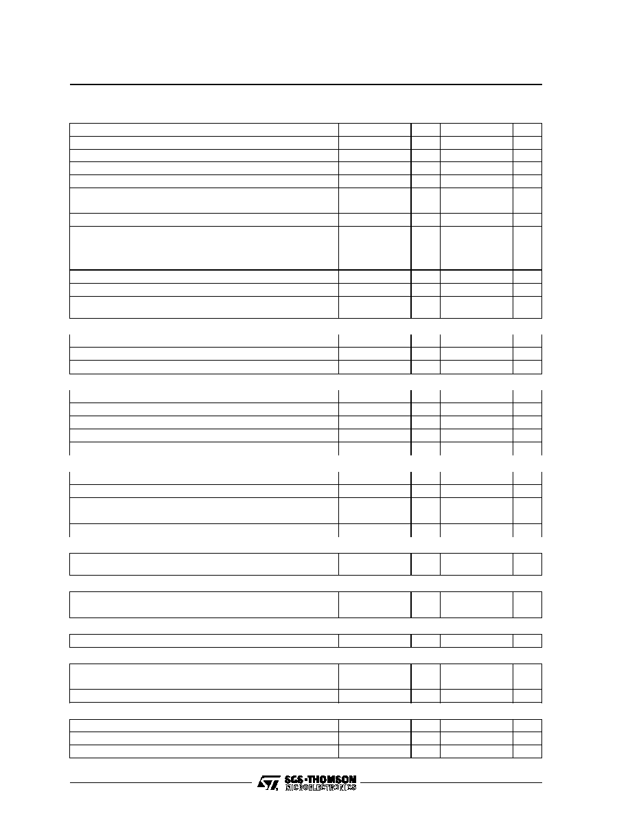
ELECTRICAL CHARACTERISTICS (T
A
= 0
o
C to 70
o
C, AV
DD
= DV
DD
= 5V, unless otherwise specified)
Symbol
Parameter
Min.
Typ.
Max.
Unit
DV
DD
Digital Supply Voltage DV
DD
- DGND
4.75
5.0
5.25
V
DI
DD
Digital Supply Current
10
mA
AV
DD
Analog Supply Voltage
4.75
5.0
5.25
V
AI
DD
Analog Supply Current
25
mA
AV
DD
-DV
DD
Analog to Digital Supply Voltage Difference
-200
0
200
mV
DV
OH
Digital Output Voltage High Level (I
LOAD
= -1mA)
DV
DD
- 0.5
V
DV
OL
Digital Output Voltage Low Level (I
LOAD
= +1mA)
DGND + 0.5
V
DV
IH
Digital Input Voltage High Level
0.75 x
(DV
DD
- DGND)
V
DV
IL
Digital Input Voltage Low Level
0.15 x
(DV
DD
- DGND)
V
DI
IH
Digital Input Current High Level
1
�
A
DI
IL
Digital Input Current Low Level
-1
�
A
BW
Bandwidth at pins : VIDEO IN, VIDEO OUT1,
VIDEO OUT2, CIN, YIN, YOUT, COUT
8.0
MHz
VIDEO IN (Pin 2)
V
SYNCIN
Sync Pulse Range
100
650
mV
V
CL
Clamp Voltage
1.10
1.25
1.4
V
C
IN
External Capacitor
2.2
�
F
VIDEO OUT1 (Pin 27)
V
OUT1
Output Dynamic Range
2.0
4.4
V
Black Level Voltage
2.6
2.85
3.1
V
C
L1
Output Capacitor Load
20
pF
R
L1
Output Resistor Load
10
k
Z
OUT1
Output Impedance
250
VIDEO OUT2 (Pin 26)
V
OUT2
Output Dynamic Range
2.0
4.4
V
Black Level Voltage
2.6
2.85
3.1
V
C
L2
Output Capacitor Load
20
pF
R
L2
Output Resistor Load
10
k
Z
OUT2
Output Impedance
250
GAIN (Pins 26- 27)
Gain Dispersion 0dB
6dB
-1
5
0
6
+1
7
dB
dB
CIN (Pin 25)
C
CIN
Input Capacitance
0.5
pF
R
CIN
Input Resistance
50
k
YIN (Pin 28)
C
YIN
Input Capacitance
0.5
pF
YOUT (Pin 1)
V
YOUT
Output Dynamic Range
0.5
3.5
V
C
LYOUT
Output Capacitor Load
15
pF
R
LYOUT
Output Resistor Load
10
k
COUT (Pin 24)
V
COUT
Output Dynamic Range
0.5
3.5
V
C
LCOUT
Output Capacitor Load
15
pF
R
LCOUT
Output Resistor Load
10
k
5730-04.TBL
STV5730
4/19
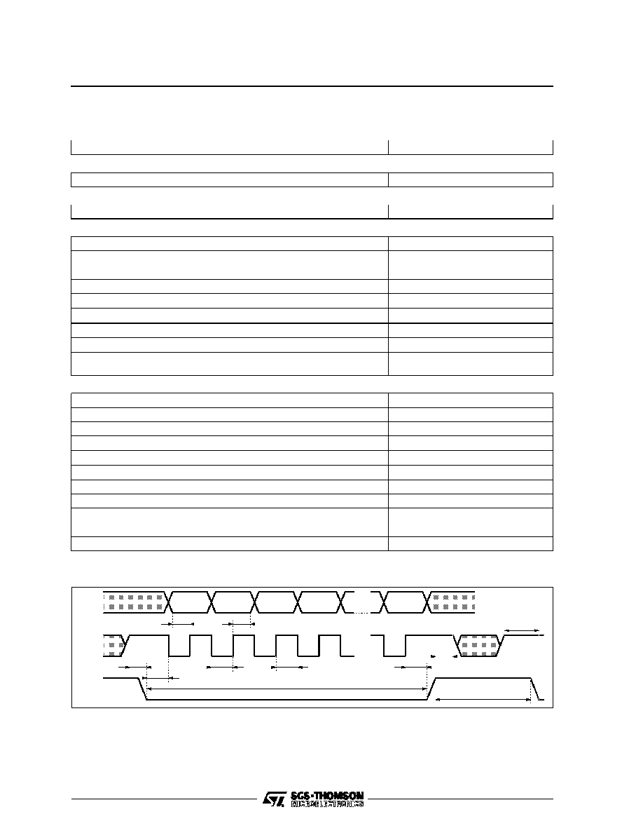
ELECTRICAL CHARACTERISTICS (T
A
= 0
o
C to 70
o
C, AV
DD
= DV
DD
= 5V, unless otherwise specified)
(continued)
Symbol
Parameter
Min.
Typ.
Max.
Unit
LESCREEN (Pin 23)
V
LESCR
Input Level
1.0
3.0
V
LECHAR (Pin 22)
V
LECH
Input Level
1.0
3.0
V
INTERNAL SIGNAL LEVELS (Pins 1- 24)
V
SYNC
Internal Sync Level
0.95
V
V
BLACK
Internal Black Level
1.1
1.25
1.4
V
V
SCREEN
Internal LESCREEN
1.4
V
V
CHAR
Internal LECHAR
1.8
V
V1
Difference Level between Black and Sync Level
250
300
350
mV
V2
Difference Level between Screen and Black Level
100
150
200
mV
V3
Difference Level between Char. and Screen Level
360
410
460
mV
V
BURSTPP
Burst Amplitude
360
mV
PP
V
CH1PP
V
CH2PP
Chroma Amplitude for blue or yellow colors
for red, magenta, green or cyan colors
360
520
mV
PP
mV
PP
BUS (Pins 11- 12 - 13)
f
CLK
CLK Frequency Range
0
2
MHz
t
CWL
CLK Width Low
200
ns
t
CWH
CLK Width High
200
ns
t
CSWL
CSN Width Low
maxHZ* x 4
�
s
t
CSWH
CSN Width High
maxHZ* x 4
�
s
t
DCLH
DATA Valid to CLK High
100
ns
t
CLD
CLK High to DATA Unvalid
100
ns
t
CLCSL
CLK Valid to CSN Low
100
ns
t
CSLCLL
CSN Low to CLK Low
100
ns
t
CLHCSH
CLK High to CSN High
100
ns
t
CSHCL
CSN High to CLK Unvalid
100
ns
5730-05.TBL
* maxHZ is the maximum horizontal zoom factor that is used
DATA
CLK
CSN
t
CSHCL
t
CSWL
t
CSLCLL
t
CWH
t
CWL
t
DCLH
t
CLCSL
t
CLD
t
CLHCSH
t
CLCSL
t
CSWH
5730-03.EPS
Figure 1
STV5730
5/19