 | –≠–ª–µ–∫—Ç—Ä–æ–Ω–Ω—ã–π –∫–æ–º–ø–æ–Ω–µ–Ω—Ç: STV6413DT | –°–∫–∞—á–∞—Ç—å:  PDF PDF  ZIP ZIP |
STV6413
Audio/Video Switch Matrix
Æ
This is preliminary information on a new product now in development. Details are subject to change without notice.
February 2004
1/28
Main Features
I≤C Bus Control
Standby Mode with Interrupt Signal Output
Video Section
3 CVBS Inputs, 2 CVBS Outputs
3 Y/C Inputs, 2 Y/C Outputs
6 dB Gain on all CVBS/Y and C Outputs
Integrated 150
W
Buffers
2 RGB/FB Inputs, 1 Tri-state RGB/FB Output
with 6 dB Adjustable Gain (from +3 dB to
+9 dB)
Video Muting on all Outputs
2 Slow Blanking Inputs/Outputs
Sync Bottom Clamp on all CVBS/Y and RGB
Inputs, Average Clamp on C Inputs
Bandwidth: 15 MHz
Crosstalk: 50 dB Minimum
Audio Section
3 Stereo Inputs, 3 Stereo Outputs
Stereo-to-Mono Sound Capability
0/6/9 dB Selectable Gain on one Stereo Input
Full Range Volume Control with Soft Control
Audio Muting on all Outputs
Description
The STV6413 is a highly integrated I≤C bus-
controlled audio and video switch matrix, optimized
for use in digital set-top box applications. It provides
the audio and video routings required in a two
SCART set-top box design.
In a TQFP64 (10 x 10 mm) package, the STV6413
is compatible with the STV6412A (TQFP64 14 x
14 mm) used for designing boards with two levels of
integration.
TQFP64
(10 x 10 x 1.40 mm)
(Thin Full Plastic Quad Flat Pack)
Order Codes:
STV6413D (Tray)
STV6413DT (Tape and Reel)

STV6413
2/28
Table of Contents
Chapter 1
General Information . . . . . . . . . . . . . . . . . . . . . . . . . . . . . . . . . . . . . . . . . . . . . . .3
1.1
I/O Pin Description ............................................................................................................ 3
Chapter 2
Electrical Characteristics . . . . . . . . . . . . . . . . . . . . . . . . . . . . . . . . . . . . . . . . . . .8
2.1
Absolute Maximum Ratings ................................................................................................ 8
2.2
Thermal Data ...................................................................................................................... 8
2.3
Latch-up Data ....................................................................................................................... 8
2.4
Electrical Characteristics ...................................................................................................... 9
Chapter 3
I≤C Bus Selection . . . . . . . . . . . . . . . . . . . . . . . . . . . . . . . . . . . . . . . . . . . . . . . . .15
3.1
I≤C Bus Addresses ............................................................................................................. 15
3.2
Power-on Reset -- Bus Register Initial Conditions ............................................................ 20
Chapter 4
Input/Output Groups . . . . . . . . . . . . . . . . . . . . . . . . . . . . . . . . . . . . . . . . . . . . . .22
Chapter 5
Application Diagram . . . . . . . . . . . . . . . . . . . . . . . . . . . . . . . . . . . . . . . . . . . . . .25
Chapter 6
Package Mechanical Data . . . . . . . . . . . . . . . . . . . . . . . . . . . . . . . . . . . . . . . . .26
Chapter 7
Revision History . . . . . . . . . . . . . . . . . . . . . . . . . . . . . . . . . . . . . . . . . . . . . . . . . .27
3/28
STV6413
General Information
1
General Information
1.1
I/O Pin Description
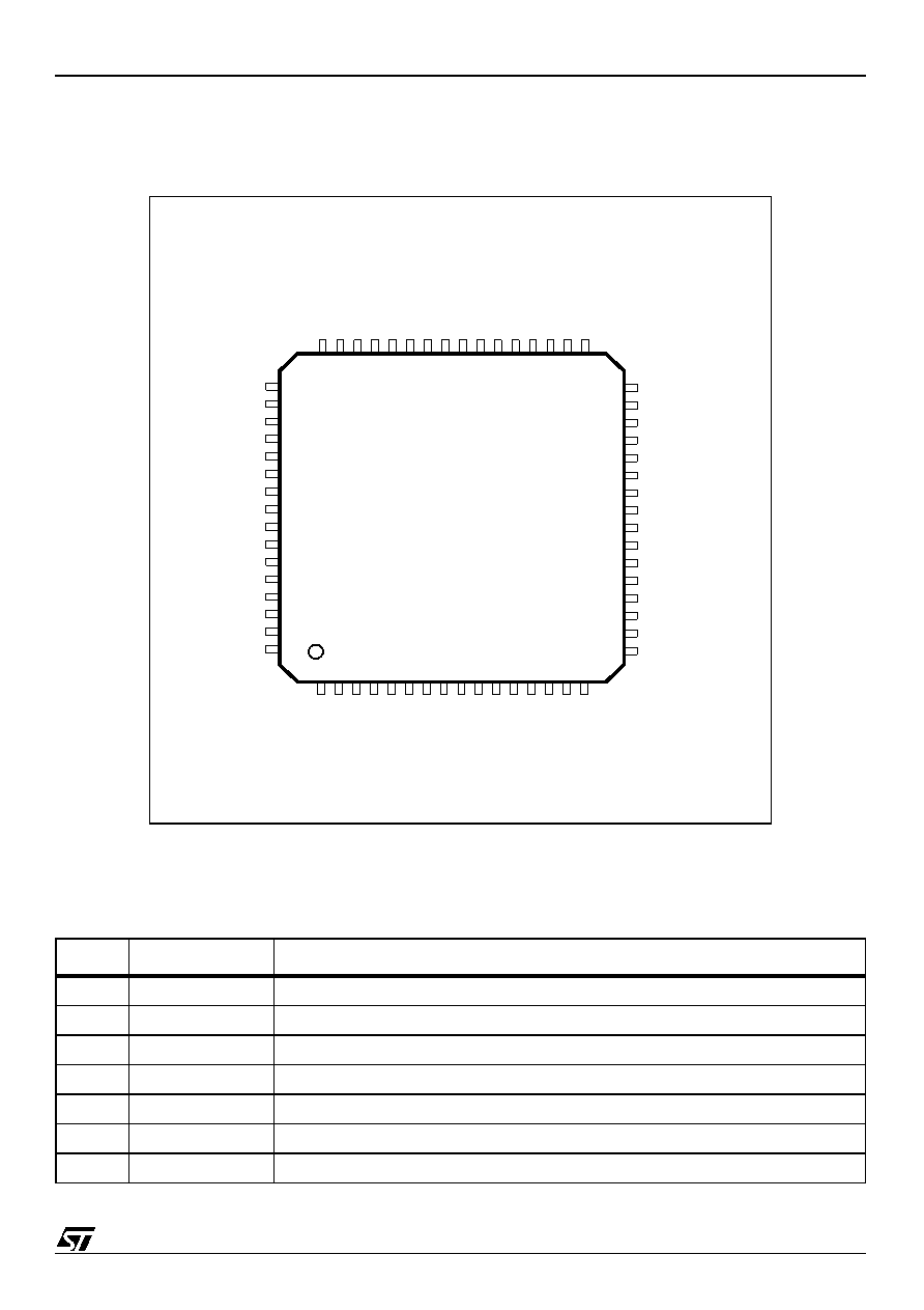
Figure 1: STV6413 Pinout Diagram
Table 1: Pin Description (Sheet 1 of 3)
Pin No.
Name
Function
1
VCC
+5 V Supply
2
NC
Not connected
3
DECV
Video Decoupling Capacitor
4
Y/CVBSIN_ENC
Y/CVBS Input from Encoder
5
GND
Ground
6
YIN_ENC
Y Input from Encoder
7
NC
Not connected
FBOUT_TV
C_GATE
VDD
NC
SCL
SDA
GND
IT_OUT
SLB_TV
R/CIN_VCR
SLB_VCR
GIN_VCR
VCC12
BIN_VCR
LO
UT
_T
V
NC
NC
NC
V
CCB
5
BO
U
T
_TV
V
CCB
4
GOUT_
T
V
GNDB
R/COUT
_T
V
V
CCB
3
Y/
C
V
B
S
O
U
T
_
TV
V
CCB
2
COUT
_V
CR
V
CCB
1
Y
/
CV
B
S
O
UT
_V
CR
ROUT_TV
VCCAO
LOUT_VCR
ROUT_VCR
LOUT_CINCH
ROUT_CINCH
NC
GNDA
VCCA
RIN_TV
LIN_TV
CVBSIN_TV
RIN_VCR
LIN_VCR
Y/CVBSIN_VCR
GND
DE
CA
NC
BI
N
_
EN
C
LI
N_E
N
C
GI
N_
ENC
RI
N_
E
N
C
R/
CIN_E
N
C
NC
CI
N_
E
N
C
NC
YI
N
_
EN
C
GND
Y
/
CV
B
S
IN_E
NC
DE
CV
NC
VC
C
STV6413
FBIN_VCR
FBIN_ENC
49
50
51
52
53
54
55
56
57
58
59
60
61
62
63
64
32
31
30
29
28
27
26
25
24
23
22
21
20
19
18
17
16
15
14
13
12
11
10
9
8
7
6
5
4
3
2
1
48
47
46
45
44
43
42
41
40
39
38
37
36
35
34
33
General Information
STV6413
4/28
8
CIN_ENC
Chroma Input from Encoder
9
NC
Not connected
10
R/CIN_ENC
Red/Chroma Input from Encoder
11
RIN_ENC
Audio Right, Input from Encoder
12
GIN_ENC
Green Input from Encoder
13
LIN_ENC
Audio Left, Input from Encoder
14
BIN_ENC
Blue Input from Encoder
15
NC
Not Connected
16
DECA
Audio Decoupling Capacitor
17
GND
Ground
18
Y/CVBSIN_VCR
Y/CVBS Input from VCR SCART
19
LIN_VCR
Audio Left, Input from VCR SCART
20
RIN_VCR
Audio Right, Input from VCR SCART
21
CVBSIN_TV
CVBS Input from TV SCART
22
LIN_TV
Audio Left, Input from TV SCART
23
RIN_TV
Audio Right, Input from TV SCART
24
VCCA
Audio Supply Voltage - or - Audio Supply Decoupling
25
GNDA
Audio Ground
26
NC
Not Connected
27
ROUT_CINCH
Audio Right Output to Cinch
28
LOUT_CINCH
Audio Left Output to Cinch
29
ROUT_VCR
Audio Right Output to VCR SCART
30
LOUT_VCR
Audio Left Output to VCR SCART
31
VCCAO
Audio Output Supply Voltage - or - Main Audio Supply Voltage
32
ROUT_TV
Audio Right Output to TV SCART
33
LOUT_TV
Audio Left Output to TV SCART
34
NC
Not connected
35
NC
Not connected
36
NC
Not connected
37
VCCB5
Video Output Buffer Supply Pin
38
BOUT_TV
Blue Output to TV SCART
39
VCCB4
Video Output Buffer Supply Pin
40
GOUT_TV
Green Output to TV SCART
41
GNDB
Video Buffer Ground
42
R/COUT_TV
Red/Chroma Output to TV SCART
Table 1: Pin Description (Sheet 2 of 3)
Pin No.
Name
Function
5/28
STV6413
General Information
43
VCCB3
Video Output Buffer Supply Pin
44
Y/CVBSOUT_TV
Y/CVBS Output to TV SCART
45
VCCB2
Video Output Buffer Supply Pin
46
COUT_VCR
Chroma Output to VCR SCART
47
VCCB1
Video Output Buffer Supply Pin
48
Y/CVBSOUT_VCR
Y/CVBS Output to VCR SCART
49
FBOUT_TV
Fast Blanking Output to TV SCART
50
FBIN_VCR
Fast Blanking Input from VCR SCART
51
FBIN_ENC
Fast Blanking Input from Encoder
52
C_GATE
External MOS Command for C_VCR bidirectional mode
53
VDD
+5 V I≤C Supply
54
NC
Not connected
55
SCL
I≤C Bus Clock
56
SDA
I≤C Bus Data
57
GND
Ground Digital
58
IT_OUT
Interrupt Output
59
SLB_TV
Slow Blanking Input/Output from TV SCART
60
R/CIN_VCR
Red Input (or C Input) from VCR SCART
61
SLB_VCR
Slow Blanking Input/Output from VCR SCART
62
GIN_VCR
Green Input from VCR SCART
63
VCC12
+12 V Supply
64
BIN_VCR
Blue Input from VCR SCART
Table 1: Pin Description (Sheet 3 of 3)
Pin No.
Name
Function