 | –≠–ª–µ–∫—Ç—Ä–æ–Ω–Ω—ã–π –∫–æ–º–ø–æ–Ω–µ–Ω—Ç: STV6435S | –°–∫–∞—á–∞—Ç—å:  PDF PDF  ZIP ZIP |
TARGET SPECIFICATION
STV6435
Filtered Video Buffers for STB and DVD Devices
Æ
This is preliminary information on a new product forseen to be developed. Details are subject to change without notice.
September 2003
1/17
FEATURES
s
Y, C, CVBS and RGB Inputs with 7 MHz Filters
s
6 dB Gains
s
Capabilities of Integrated Output Buffers:
Single Load (150
) for RGB signals
Double Load (75
) for Y, C and CVBS signals
s
DC Coupled Outputs for CVBS and RGB
signals, DC or AC coupled output for Chroma
signal
s
Bottom Clamp on RGB, Y and CVBS, Bias
Clamp on C
s
Crosstalk: 55 dB (typ.)
s
Separate Stand-by Modes on Y/C/CVBS and
on RGB signals
s
Switchable Y+C Adder for Decoders without
CVBS Outputs
DESCRIPTION
The STV6435 is a filtered video output interface for
STB and DVD applications.
After removing D/A conversion noises using
integrated low pass filters, the STV6435 adapts in
amplitude and impedance the video signals coming
from the digital decoder for transmission, via 75
adapted cables, to the TV set, VCR and auxiliary
devices.
The STV6435 is powered by a 5V supply.
The STV6435 is fully compatible with STi55xx
Digital Decoders.
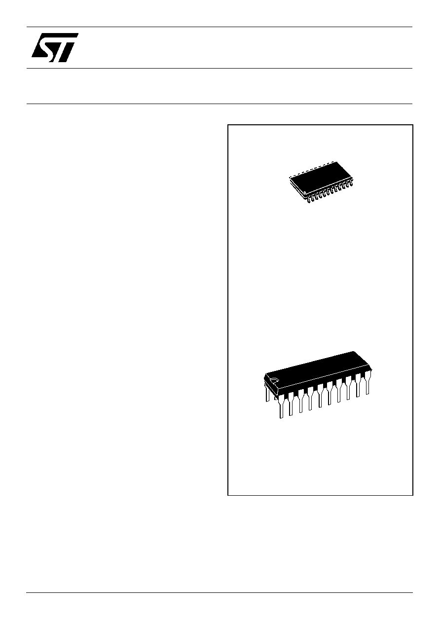
The STV6435 is mounted in a SO24 package
(STV6435S) or in a DIP package (STV6435D).
Order Code: STV6435D
PDIP20
Order Code: STV6435S
SO24

STV6435
2/17
Table of Contents
Chapter 1
General Information . . . . . . . . . . . . . . . . . . . . . . . . . . . . . . . . . . . . . . . . . . . . . . .3
1.1
I/O Pin Description ............................................................................................................. 4
Chapter 2
Electrical Characteristics . . . . . . . . . . . . . . . . . . . . . . . . . . . . . . . . . . . . . . . . . . .6
2.1
Absolute Maximum Ratings ................................................................................................ 6
2.2
Thermal Data ...................................................................................................................... 6
2.3
Electrical Characteristics ...................................................................................................... 6
Chapter 3
Input/Output Groups . . . . . . . . . . . . . . . . . . . . . . . . . . . . . . . . . . . . . . . . . . . . . .10
Chapter 4
Application Diagram . . . . . . . . . . . . . . . . . . . . . . . . . . . . . . . . . . . . . . . . . . . . . .13
Chapter 5
Package Mechanical Data . . . . . . . . . . . . . . . . . . . . . . . . . . . . . . . . . . . . . . . .14
Chapter 6
Revision History . . . . . . . . . . . . . . . . . . . . . . . . . . . . . . . . . . . . . . . . . . . . . . . . . .16
3/17
STV6435
General Information
1
General Information
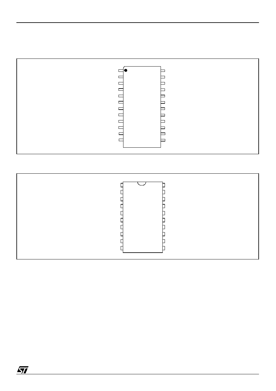
Note:
The three RGB channels are identical and their pin assignments may be interchanged in an
application if needed. In this case, verify that the outputs correspond to the inputs; for example, the
pin 7 input must correspond to the pin 14 output.
Figure 1: STV6435S Pinout
Figure 2: STV6435D Pinout
15
16
24
23
22
21
20
19
18
17
1
2
3
4
5
6
7
8
9
10
13
14
11
12
CVBS_ENC
DEC
C_ENC
GND
Y_ENC
GND
GND
VCC
G_ENC
R_ENC
MUTE
B_ENC
VCCB3
CVBSOUT
VCCB2
COUT
GNDB
GND
GND
YOUT
GOUT
VCCB1
ROUT
BOUT
1
2
3
4
5
6
7
8
9
10
11
12
20
19
18
17
16
15
14
13
CVBS_ENC
DEC
C_ENC
GND
Y_ENC
VCC
G_ENC
R_ENC
MUTE
B_ENC
VCCB3
CVBSOUT
VCCB2
COUT
GNDB
YOUT
GOUT
VCCB1
ROUT
BOUT
General Information
STV6435
4/17
1.1
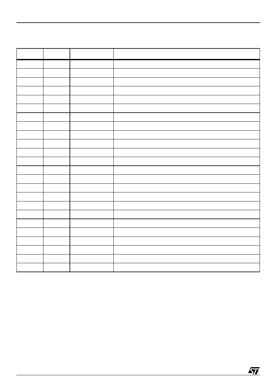
I/O Pin Description
Table 1: Pin Description
STV6435S STV6435D
Name
Function
1
1
CVBS_ENC
CVBS Input from Encoder command internal CVBS switch
2
2
DEC
Decoupling Capacitor
3
3
C_ENC
Chroma Input from Encoder
4
4
GND
Ground
5
5
Y_ENC
Y Input from Encoder
6
GND
Ground
7
GND
Ground
8
6
VCC
+5 V Supply
9
7
G_ENC
Large-band Y Input from Encoder
10
8
R_ENC
Large-band R Input from Encoder
11
9
MUTE
4-State command for Mute
12
10
B_ENC
Large-band B Input from Encoder
13
11
BOUT
B Output
14
12
ROUT
R Output
15
13
VCCB1
+5 V Supply for Output Buffers
16
14
GOUT
G Output
17
15
YOUT
Y Output
18
GND
Ground
19
GND
Ground
20
16
GNDB
Ground for Buffers
21
17
COUT
Chroma Output
22
18
VCCB2
+5 V Supply for Output Buffers
23
19
CVBSOUT
CVBS Output
24
20
VCCB3
+5 V Supply for Output Buffers
5/17
STV6435
General Information
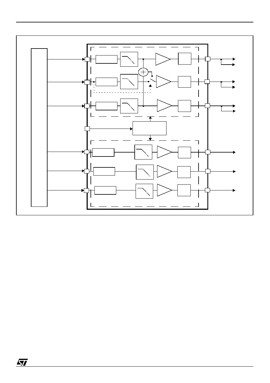
Figure 3: STV6435 Block Diagram
Dig
ita
l
En
co
d
e
r
C_ENC
COUT
CVBSOUT
Y_ENC
YOUT
G_ENC
Bot. Clamp
R_ENC
B_ENC
7 MHz
4th order
G_OUT
R_OUT
B_OUT
Buffer
MUTE
CVBS_ENC
Buffer
Buffer
Buffer
Buffer
Buffer
6 dB
6 dB
6 dB
6 dB
6 dB
6 dB
7 MHz
4th order
7 MHz
4th order
7 MHz
4th order
7 MHz
4th order
7 MHz
4th order
Bot. Clamp
Bot. Clamp
Av. Clamp
Mute
Bot. Clamp
Bot. Clamp