 | –≠–ª–µ–∫—Ç—Ä–æ–Ω–Ω—ã–π –∫–æ–º–ø–æ–Ω–µ–Ω—Ç: STV6618 | –°–∫–∞—á–∞—Ç—å:  PDF PDF  ZIP ZIP |
September 2003
1/24
Æ
Main Features
s
I≤C Bus Control
s
5 Y/CVBS Inputs, 3 Y/CVBS Outputs
s
3 C Inputs, 1 C Output
s
2 RGB/YPrPb Inputs, 1 RGB/YPrPb Output
s
6 dB Gain on all 150
Buffer Outputs
s
Integrated 150
Buffers
s
Video Muting on all Outputs
s
Bottom Clamp on all CVBS/Y, Average
Clamp on C Inputs, Bottom Clamp on RGB,
Sync-tip Clamp on PrPb signals
s
Bandwidth: 17 MHz
s
Crosstalk: 50 dB
Description
The STV6618 is a highly integrated I≤C bus-
controlled video switch matrix, optimized for use in
recordable Digital Video Disk applications or DVD
players. It is adapted to video signals with 1H and
2H formats video routings. It provides required for
connections to two external devices (Europe 2
SCARTs), internal tuners, digital encoders and
recorders.
TQFP44
(10 x 10 x 1.4 mm)
(Thin Full Plastic Quad Flat Pack)
ORDER CODE: STV6618
STV6618
Video Switch Matrix for DVDs

STV6618
2/24
Table of Contents
Chapter 1
GENERAL OVERVIEW . . . . . . . . . . . . . . . . . . . . . . . . . . . . . . . . . . . . . . . . . . . . . .3
1.1
Pin Connections .................................................................................................................. 3
1.2
Pin Description ................................................................................................................... 4
Chapter 2
ELECTRICAL CHARACTERISTICS . . . . . . . . . . . . . . . . . . . . . . . . . . . . . . . . . . . .7
2.1
Absolute Maximum Ratings ................................................................................................ 7
2.2
Thermal Data ...................................................................................................................... 7
2.3
Recommended Operating Conditions .................................................................................. 7
2.4
Video Section Characteristics .............................................................................................. 8
2.5
Fast Blanking Section Characteristics ................................................................................. 9
2.6
Chroma Section Characteristics ......................................................................................... 10
2.7
Digital Outputs .................................................................................................................... 10
2.8
I≤C Bus Characteristics ...................................................................................................... 11
Chapter 3
I≤C BUS SELECTION . . . . . . . . . . . . . . . . . . . . . . . . . . . . . . . . . . . . . . . . . . . . . .12
3.1
I≤C Bus Addresses ............................................................................................................. 12
3.2
Power-on Reset: Bus Register Initial Conditions ............................................................... 15
Chapter 4
INPUT/OUTPUT GROUPS . . . . . . . . . . . . . . . . . . . . . . . . . . . . . . . . . . . . . . . . . .16
Chapter 5
APPLICATION DIAGRAMS . . . . . . . . . . . . . . . . . . . . . . . . . . . . . . . . . . . . . . . .20
Chapter 6
PACKAGE MECHANICAL DATA . . . . . . . . . . . . . . . . . . . . . . . . . . . . . . . . . . . .22
Chapter 7
REVISION HISTORY . . . . . . . . . . . . . . . . . . . . . . . . . . . . . . . . . . . . . . . . . . . . . . .23
3/24
STV6618 GENERAL
OVERVIEW
1
GENERAL OVERVIEW
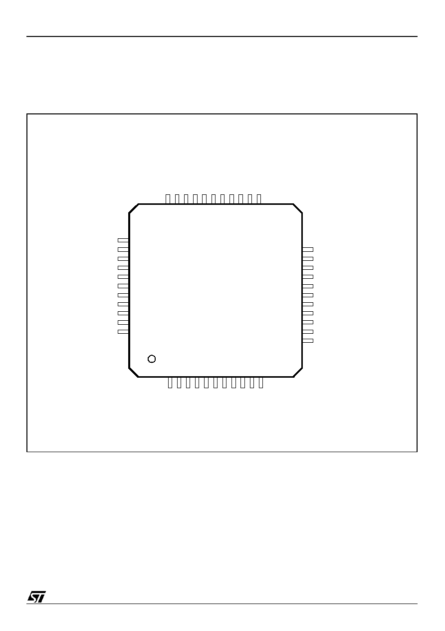
1.1
Pin Connections
Figure 1: Pinout Diagram
FBOUT_TV
FBIN_AUX
VDD
SCL
SDA
GNDD
CIN_TV
Y/CVBSIN_TV
DIGOUT1
CIN_TUN
Y/C
V
B
S
O
U
T
_
T
V
V
CCB
3
R/P
R
/
C
O
U
T
_
T
V
V
CCB
2
G/
Y
O
U
T
_
T
V
C_
G
A
T
E
B/
PBO
U
T
_
T
V
G
NDB
Y/C
V
B
S
O
U
T
_
AU
X
V
CCB
1
C
O
UT
_
A
UX
Y/CVBSOUT_REC
VCCB_REC
Y/CVBSIN_AUX
R/PR/CIN_AUX
DIGOUT5
G/YIN_AUX
B/PBIN_AUX
GND2
B/P
B
IN
_
E
N
C
G
/
YI
N
_
EN
C
R/
P
R
/CI
N
_
E
NC
VC
C
YI
N
_
EN
C
CI
N
_
E
N
C
DE
CV
C
VBSI
N
_
EN
C
12
13
14
15
16
17
18
19
20
21
22
23
24
25
26
27
28
29
30
31
32
33
34
35
36
37
38
39
40
41
42
43
44
DIGOUT2
DIGOUT4
DIGOUT6
GNDB_REC
11
10
9
8
7
6
5
4
3
2
1
G
ND1
DI
G
O
UT
3
Y/
C
V
BSI
N
_
T
U
N
GENERAL OVERVIEW
STV6618
4/24
1.2
Pin Description
Pin No.
Symbol
Description
1
Y/CVBSIN_TUN
Y/CVBS Input from Tuner
2
DIGOUT3
Digital Output Pin 3
3
GND1
Ground Supply 1 for Video Inputs
4
CVBSIN_ENC
CVBS Input from Encoder
5
DECV
Video decoupling capacitor
6
CIN_ENC
Chroma Input from Encoder
7
YIN_ENC
Y Input from Encoder
8
V
CC
+5 V Power Supply for Video Inputs
9
R/PR/CIN_ENC
Red or Pr or Chroma Input from Encoder
10
G/YIN_ENC
Green or Y Input from Encoder
11
B/PBIN_ENC
Blue or Pb Input from Encoder
12
GND2
Ground Supply 2 for Video Inputs
13
B/PBIN_AUX
Blue or Pb Input from Auxiliary (SCART2 or external Cinch)
14
DIGOUT4
Digital Output Pin 4
15
G/YIN_AUX
Green or Y Input from Auxiliary (SCART2 or external Cinch)
16
DIGOUT5
Digital Output Pin 5
17
R/PR/CIN_AUX
Red or Pr or Chroma input from Auxiliary (SCART2 or external Cinch)
18
DIGOUT6
Digital Output Pin 6
19
Y/CVBSIN_AUX
Y/CVBS Input from Auxiliary (SCART2 or external Cinch)
20
VCCB_REC
Video Output Recorder Buffer Supply Pin
21
Y/CVBSOUT_REC
Y/CVBS Output to Recorder
22
GNDB_REC
Ground Supply for Recorder Buffer
23
COUT_AUX
Chroma Output to Auxiliary (SCART2 or external Cinch)
24
VCCB1
Video Output Buffer Supply Pin
25
Y/CVBSOUT_AUX
Y/CVBS Output to Auxiliary (SCART2 or external Cinch)
26
GNDB
Ground Supply for Video Buffer
27
B/PBOUT_TV
Blue or Pb Output to TV (SCART1 or external Cinch)
28
C_GATE
External Transistor Command for Bidirectinnal B/C SCART I/O
29
G/YOUT_TV
Green or Y Output to TV (SCART1 or external Cinch)
30
VCCB2
Video Buffer
31
R/PR/COUT_TV
Red or Pr or Chroma Output to TV (SCART1 or external Cinch)
32
VCCB3
Video Output Buffer Supply Pin
33
Y/CVBSOUT_TV
Y/CVBS Output to TV (SCART1 or external Cinch)
34
FBOUT_TV
Fast Blanking Output to TV (SCART1)
35
FBIN_AUX
Fast Blanking Input from Auxiliary (SCART2)
5/24
STV6618 GENERAL
OVERVIEW
36
VDD
+5 V Digital Power Supply
37
SCL
I≤C Bus Clock
38
SDA
I≤C Bus Data
39
GNDD
Digital Ground Supply
40
CIN_TV
Chroma Input from TV (SCART1 or external Cinch)
41
Y/CVBSIN_TV
Y/CVBS Input from TV (SCART1 or external Cinch)
42
DIGOUT1
Digital Output Pin 1
43
CIN_TUN
Chroma Input from Tuner
44
DIGOUT2
Digital Output Pin 2
Figure 2: STV6618 Input/Output Diagram
Pin No.
Symbol
Description
SCART1
TV
R/PR/COUT_TV
G/YOUT_TV
B/PBOUT_TV
FBOUT_TV
Y/CVBSOUT_TV
Y/CVBSIN_TV
Tuner
Y/CVBSIN_TUN
Encoder
R/PR/CIN_ENC
G/YIN_ENC
B/PBIN_ENC
CVBSIN_ENC
CIN_ENC
YIN_ENC
Recorder
Y/CVBS_REC
SCART2
R/PR/CIN_AUX
G/YIN_AUX
B/PB_AUX
FBIN_AUX
Y/CVBSIN_AUX
COUT_AUX
COUT_REC
CIN_TV
Transistor
C_GATE
STV6618
(TQFP 44)
DIGOUT1
DIGOUT2
Y/CVBSOUT_AUX
CIN_TUN
DIGOUT3
DIGOUT4
DIGOUT5
DIGOUT6
(Auxiliary)
GENERAL OVERVIEW
STV6618
6/24
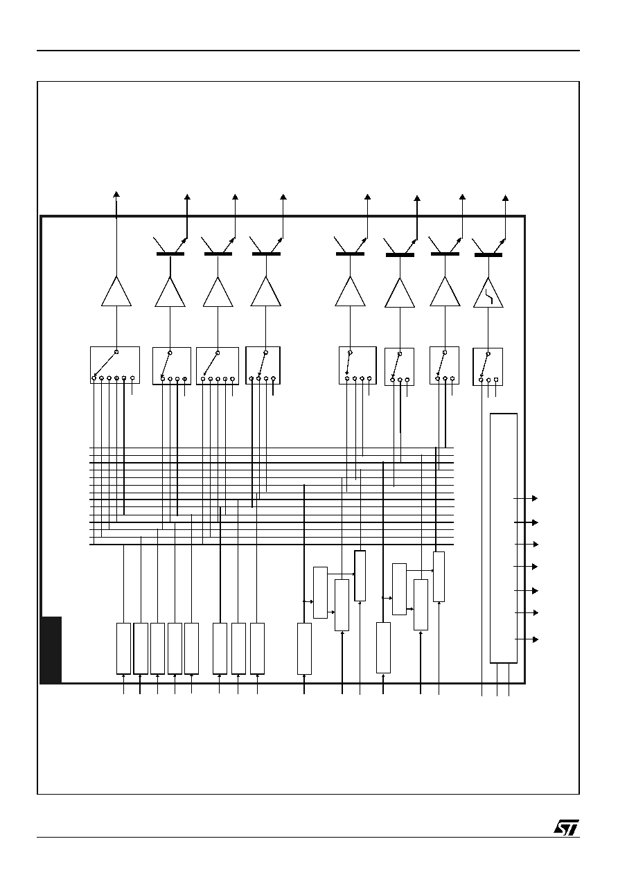
Figure 3: STV6618 Block Diagram
Y/
C
VBSI
N
_
T
U
N
Y/
C
V
B
S
I
N
_
T
V
Y/
C
VBSI
N
_
AU
X
C
VBSI
N
_
EN
C
G
/
YI
N
_
AU
X
R
/
P
R
/C
IN
_A
U
X
B/
PBI
N
_
AU
X
G
/
YI
N
_
EN
C
R
/
P
R
/C
IN
_E
N
C
B/
PBI
N
_
EN
C
YI
N
_
EN
C
CI
N
_
T
V
CI
N_
E
N
C
mu
t
e
0 d
B
Y/
C
VBSO
U
T
_
R
EC
STV6
6
1
8
Re
co
r
d
e
r
mu
t
e
6 dB
Y/
C
VBSO
U
T
_
T
V
SC
AR
T
1
mu
t
e
6 d
B
Y/
C
VBSO
U
T
_
A
U
X
SC
AR
T
2
mu
t
e
6 d
B
R
/
P
r
/
C
O
U
T_
TV
mu
t
e
6 d
B
G/
Y
O
U
T
_
T
V
SC
AR
T
1
SC
AR
T
1
mu
t
e
6 d
B
B
/
P
b
O
U
T_
TV
SC
AR
T
1
Y/CVBS_TUN
Y/CVBS_TV
Y/CVBS_AUX
CVBSIN_ENC
YIN_ENC
CIN_TV
CIN_ENC
G/YIN_ENC
G/YIN_AUX
R/Pr/CIN_AUX
B/PbIN_AUX
R/Pr/CIN_ENC
B/PbIN_ENC
F
B
O
U
T_
TV
SC
L
FB
I
N
_
A
U
X
0v
5v
SD
A
C_GATE
I
≤C B
u
s
CV
B
S
I
N
_T
UN
Y/
C
V
B
S
I
N
_
T
V
Y
/
CV
B
S
I
N
_A
UX
CV
B
S
I
N
_E
N
C
YI
N
_
EN
C
mu
t
e
6 d
B
CO
UT
_
A
UX
Y
/
CV
B
S
I
N
_A
UX
CV
B
S
I
N
_
E
NC
YI
N
_
E
N
C
CV
B
S
I
N
_T
UN
Y/
C
V
B
S
I
N
_
T
V
CV
B
S
I
N
_E
N
C
YI
N
_
EN
C
CI
N
__T
V
CI
N_
E
N
C
CI
N_
E
N
C
R/
P
r
/
C
I
N
_A
UX
R/
P
r
/
CI
N_
E
N
C
G/Y
IN
_
A
U
X
G
/
YI
N
_
EN
C
B/
Pb
I
N
_
A
U
X
B/
P
b
I
N
_
E
N
C
FB
IN
_
A
U
X
CI
N_
T
U
N
CIN_TUN
CI
N__T
UN
DIGOUT1
DIGOUT2
DIGOUT3
DIGOUT4
DIGOUT5
DIGOUT6
Bo
. Cl
a
m
p
Bo
. Cl
a
m
p
Bo
. Cl
a
m
p
Bo
. Cl
a
m
p
Bo
. Cl
a
m
p
Av
. Cl
a
m
p
Av
. Cl
a
m
p
Av
. Cl
a
m
p
Bo
. Cl
a
m
p
Bo
.
C
l
a
m
p
Sy
n
c
S
e
p
.
Bo
t/Sy
n
c
/
A
v
.
Bo
. /
Sy
n
c
S
y
nc
S
e
p.
Bo
t
/
Sy
n
c
/Av
.
Bo
. /
Sy
n
c
7/24
STV6618 ELECTRICAL
CHARACTERISTICS
2
ELECTRICAL CHARACTERISTICS
2.1
Absolute Maximum Ratings
2.2
Thermal Data
2.3
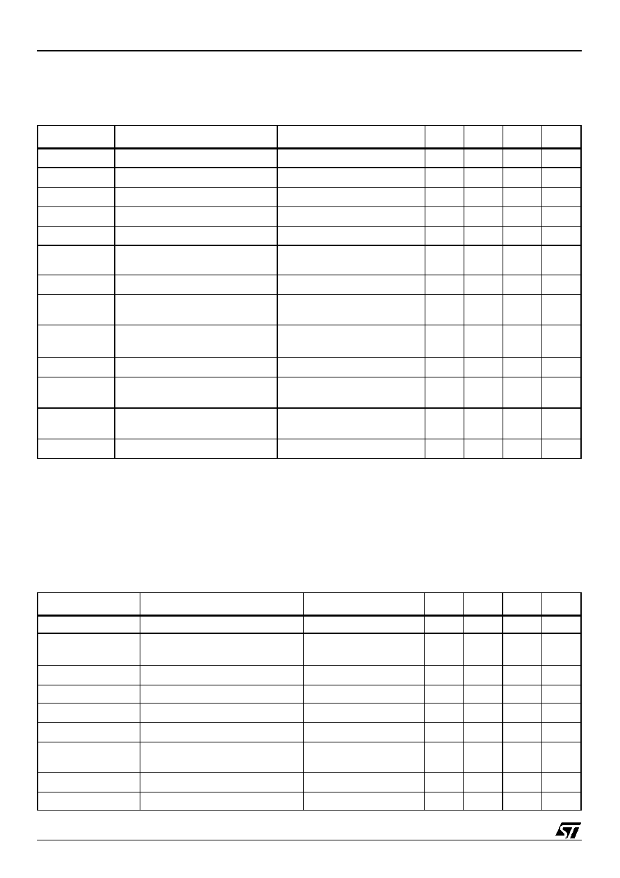
Recommended Operating Conditions
T
AMB
= 25 ∞C, V
CCV
= 5 V, V
DD
= 5 V, R
OUT_VREC
= 4.7 k
, R
OUT_VBUF
= 150
, unless otherwise
specified. Output impedances of sources: R
GV
= 75
.
Symbol
Parameter
Value
Unit
V
DD
Digital Section
6
V
V
CCV
Video Section
6
V
V
I
Voltage at Pin 1 to GND
- Video pins
- Bus pins, DIGOUT1,2,3 and C_GATE
0, 5.5
0, 5.5
V
V
DIGOUT4-5-6
Voltage at pin DIGOUT4-5-6
0, 13
V
V
ESD
Maximum ESD voltage allowed. 100 pF capacitor discharged through
1.5 k
serial resistor (Human Body Model)
±4
kV
T
OPER
Operating Ambient Temperature
0, +70
∞C
T
STG
Storage Temperature
-20, +150
∞C
Symbol
Parameter
Value
Unit
R
thJA
Junction-ambient Thermal Resistance (Maximum) on a single-layer
board
70
∞C/W
Symbol
Parameter
Test Conditions
Min.
Typ.
Max.
Unit
Supply Voltages
V
DD
Digital Supply Voltage
4.75
5.00
5.25
V
V
CCV
Video Operating Supply Voltage
4.75
5.00
5.25
V
Active Mode (All channels ON)
I
DD
Digital Supply Current
V
DD
= 5 V,
3.5
5.0
6.5
mA
I
CCV
Total Video Supply Current
V
CCV
= 5 V, No Load
31
45
58
mA
Standby Mode (All channels OFF)
I
DD
Digital Supply Current
V
DD
= 5 V
3.0
4.5
6.0
mA
I
CCVSTD
Total Video Supply Current
V
CC
= 5 V
0.5
1.0
mA
ELECTRICAL CHARACTERISTICS
STV6618
8/24
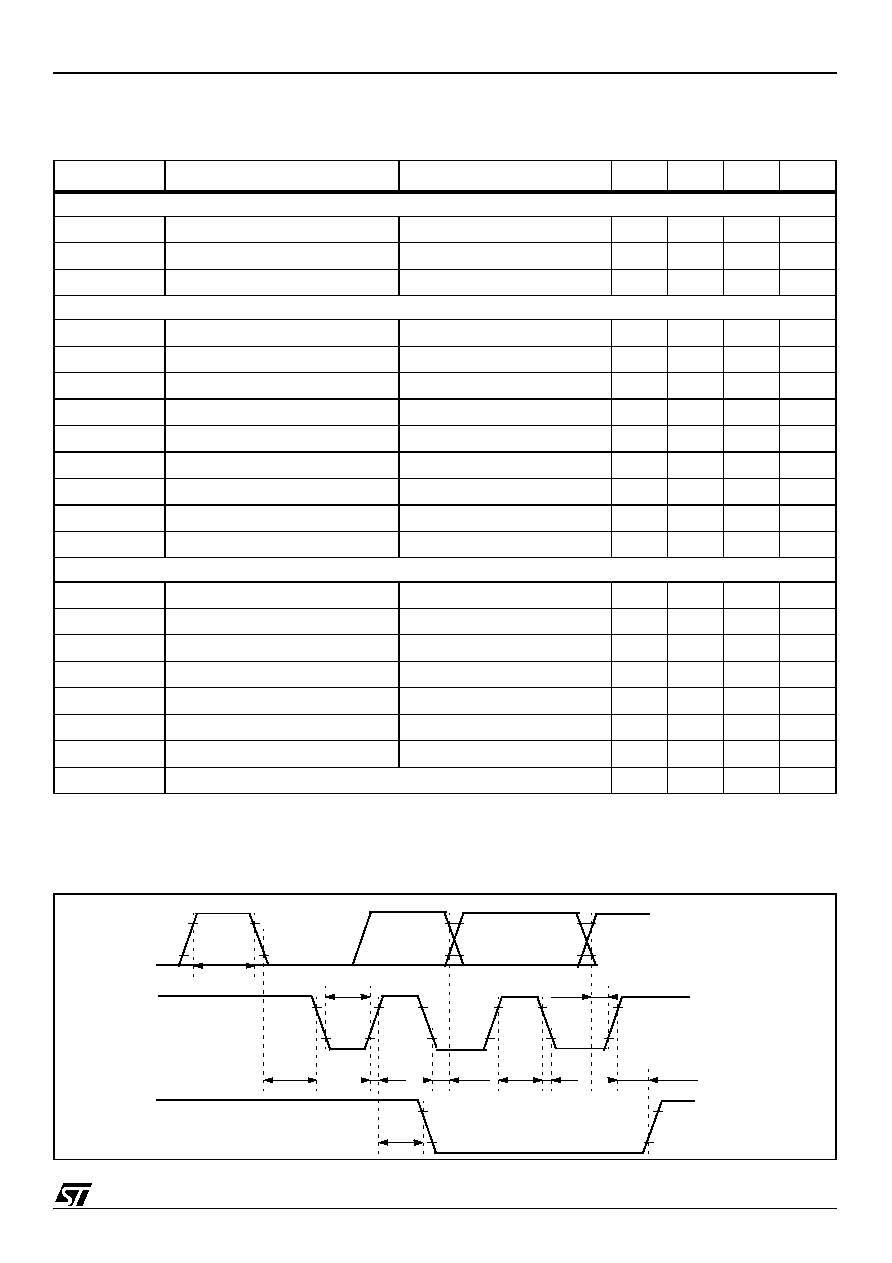
2.4
Video Section Characteristics
T
AMB
= 25 ∞C, V
CCV
= 5 V, V
DD
= 5 V, R
OUT_VREC
= 4.7 k
, R
OUT_VBUF
= 150
, unless otherwise
specified. Output impedances of sources: R
GV
= 75
.
Symbol
Parameter
Test Conditions
Min.
Typ.
Max.
Unit
V
DCIN_BOT
DC Input Level
Bottom Sync Pulse
1.9
2.0
2.2
V
I
CLAMP_BOT
Clamping Current, Bottom clamp
at V
DCIN
- 400 mV
1
2
3
mA
I
LEAK
Input Leakage Current
V
IN
= V
DCIN
+ 1 V,
Bottom clamp input
1
5
µA
V
DCIN_YSYNC
DC Input Level
Y input, YPrPb mode, Black Level
2.2
2.3
2.5
V
V
DCIN_SYNC
DC Input Level
Sync clamp input (Pr,Pb)
Sync signal on Y input
2.9
3.0
3.1
V
I
CLAMP_SYNC
Max. Clamping Current during Sync
Clamp
Sync clamp input (Pr,Pb)
at V
DCIN
- 400 mV
100
µA
C
IN
Input Capacitance
2
pF
V
IN
Maximum Input Signal
Y/CVBS, RGB
Pr, Pb
1.5
1.0
V
PP
DYN
Dynamic Output Signal
Y/CVBS, RGB
Pr, Pb
3
2
V
PP
BW
Bandwidth at -3 dB
Y/CVBS OUT
RGB OUT
Pr/Pb OUT
V
IN
= 0.7 V
PP
V
IN
= 0.7 V
PP
V
IN
= 0.7 V
PP
14
14
14
17
17
17
MHz
Flatness
Video Band Gain Spread
(15 kHz to 5 MHz)
Y/CVBS OUT
RGB OUT
Pr/Pb OUT
V
IN
= 1 V
PP
V
IN
= 1 V
PP
V
IN
= 0.7 V
PP
±0.5
±0.5
±0.5
dB
CTi
Crosstalk Isolation between Input
Channel
V
IN
= 1 V
PP
at 4.43 MHz on 1 point
54
1
60
dB
CTo
Crosstalk Isolation between Output
Channel
V
IN
= 1 V
PP
at 4.43 MHz on 1
point, R
LOAD
= 150
50
1
55
dB
R
OUT
Output Resistance
5
10
G0V
Gain at video outputs (0 dB), recorder
output
V
IN
= 1 V
PP
and Gain = 0 dB at
1 MHz
-0.5
0.0
0.5
dB
G6V
Gain at video outputs (6 dB)
V
IN
= 1 V
PP
and Gain = 6 dB at
1 MHz
5.5
6.0
6.5
dB
RGBmatch
Gain matching Between RGB outputs
V
IN
= 0.7 V
PP
and Gain = 6 dB at
1 MHz
-0.3
0.3
dB
DC
OUTZY/CVSS
DC Output Voltage,
TV and AUX Y/CVBS outputs
Bottom Sync Pulse
2
Mute
2
0.32
0.57
0.40
0.60
0.43
0.67
V
DC
OUTREC
DC Output Voltage,
Recorder Y/CVBS Output
Bottom Sync Pulse
2
Mute
2
1.2
1.3
1.3
1.4
1.4
1.5
V
9/24
STV6618 ELECTRICAL
CHARACTERISTICS
2.5
Fast Blanking Section Characteristics
DC
OUTRGB
DC Output Voltage, RGB outputs
Black Level
2
Mute
2
0.45
0.50
0.60
0.60
0.70
0.70
V
DC
OUTYOUT
DC Output Voltage, TV Y Output (G/
YOUT_TV, YPrPb mode)
Bottom Sync Pulse
2
Mute
2
0.50
0.45
0.60
0.60
0.70
0.70
V
DC
OUTPrPb
DC Output Voltage, PrPb outputs
Black Level
2
Mute
2
1.4
1.4
1.5
1.5
1.6
1.6
V
DPHI
Differential Phase, Y/CVBS
V
IN
= 1 V
PP
at 4.43 MHz
0.2
2.5
deg.
DG
Differential Gain, Y/CVBS
V
IN
= 1 V
PP
at 4.43 MHz
0.3
5
%
Mute
Mute Suppression
V
IN
= 1 V
PP
at 5 MHz on 1 point
-55
dB
LNL
Luminance non-linearity
0.3
3
%
VSN
Video Signal-to-Noise Ratio
3
75
dB
1. Minimum Crosstalk values estimated during Qualification phase, based on ST Evaluation Board
measurement, TQFP44 package soldered on board.
2. Measured at IC output pin.
3. Signal-to-Noise = 20log (VOUTblack-to-white = 0.7 V
PP
/ Vnoise(mVrms) weighted CCIR 567)
Symbol
Parameter
Test Conditions
Min.
Typ.
Max.
Unit
INPUT MODE
FB
LOW/HIGH
Input Low/High Level Threshold
0.4
0.7
0.9
V
I
IN
Input Current
2
10
µA
OUTPUT MODE
FB
LOW
Output Low Level
R
LOAD
= 150
0.5
V
FB
HIGH
Output High Level
R
LOAD
= 150
3.0
3.4
3.8
V
FB
DEL
Fast Blanking RGB delay
At 50% on digital RGB
transients, at 2 V on FB rise
transient, at 1 V on FB fall,
C
LOAD
= 10 pF maximum
15
ns
FB
TRANS
FB Transitions at FB output
Rise Time
Fall Time
C
LOAD
= 10 pF maximum
between 10% and 90%
between 90% and 10%
10
10
ns
Symbol
Parameter
Test Conditions
Min.
Typ.
Max.
Unit
ELECTRICAL CHARACTERISTICS
STV6618
10/24
2.6
Chroma Section Characteristics
T
AMB
= 25 ∞C, V
CCV
= 5 V, V
DD
= 5 V, R
OUT_VREC
= 4.7 k
, R
OUT_VBUF
= 150
,
unless otherwise
specified. Output impedances of sources: R
GV
= 75
.
2.7
Digital Outputs
T
AMB
= 25 ∞C, V
CCV
= 5 V, V
DD
= 5 V.
Symbol
Parameter
Test Conditions
Min.
Typ.
Max.
Unit
V
DCIN
DC Input Level
2.9
3.0
3.1
V
R
IN
Input Resistance
30
50
k
C
IN
Input Capacitance
2
pF
V
IN
Max Input Signal
1.0
V
PP
DYN
Dynamic Output Signal
2.0
V
PP
DC
OUT
DC Output Voltage
AUX C Output
No Chroma input signal
1
1. Measured at IC output pin.
1.4
1.5
1.6
V
CBW
Chroma Bandwidth
V
IN
= 1 V
PP
at -3 dB
10
15
MHz
CTi
Crosstalk Isolation between Input
Channel
V
IN
= 1 V
PP
at 4.43 MHz,
on one input
54
2
2. Minimum Crosstalk values estimated during Qualification phase, based on ST Evaluation Board
measurement, TQFP44 package soldered on board.
60
dB
CTo
Crosstalk Isolation between Output
Channel
V
IN
= 1 V
PP
at 4.43 MHz,
on one input, R
LOAD
= 150
50
2
55
dB
R
OUT
Output Resistance
5
10
G6C
Gain at Chroma Outputs
V
IN
= 1 V
pp
and Gain = 6 dB at
1 MHz
5.5
6.0
6.5
dB
Mute
Mute Suppression
V
IN
= 1 V
PP
at 4.43 MHz, on one
input
-55
dB
CToYdel
Chroma to Luma Delay, Source Y/C
V
IN
= V
PP
at 4.43 MHz
20
ns
Symbol
Parameter
Test Conditions
Min.
Typ.
Max.
Unit
C_gate_H
Pull-up resistor value to VccB3
16
20
24
k
C_gate_L
Output Low level
I
IN
= 0 mA
I
IN
= 1 mA
0.3
0.7
V
C_gate_H
Output High level
R
LOAD
= 20 k
V
DD
V
DIGOUT1-2-3 Load
External pull-up resistor value to VDD
10
k
DIGOUT1-2-3 Low
Output low level, DIGOUT1-2-3
R
LOAD
= 10 k
0.7
V
DIGOUT1-2-3 Middle
Output middle level, DIGOUT1-2-3
R
LOAD
= 10 k
2.2
V
DIGOUT1-2-3 High
Output high level,DIGOUT1-2-3
R
LOAD
= 10 k
,
Opened collector output
V
DD
V
DIGOUT4-5-6 Low
Output low level, DIGOUT4-5-6
I
LOAD
= 2 mA
0.7
V
DIGOUT4-5-6 High
Output high level, DIGOUT4-5-6
Opened Collector Output
13
V
11/24
STV6618 ELECTRICAL
CHARACTERISTICS
2.8
I≤C Bus Characteristics
T
AMB
= 25 ∞C, V
CCV
= 5 V, V
DD
= 5 V
Note:
The device can also operate at 400 kHz and can interface with +3.3 V or + 5 V logic levels.
Symbol
Parameter
Test Conditions
Min.
Typ.
Max.
Unit
SCL
V
IL
Low Level Input Voltage
-0.3
1.5
V
V
IH
High Level Input Voltage
2.3
5.5
V
I
LI
Input Leakage Current
V
IN
= 0 to 5.5 V
-10
0
10
µs
SDA
V
IL
Low Level Input Voltage
-0.3
1.5
V
V
IH
High Level Input Voltage
2.3
5.5
V
I
LI
Input Leakage Current
V
IN
= 0 to 5.5 V
-10
0
10
µs
C
I
Input Capacitance
10
pF
t
R
Input Rise Time
1.5 V to 3 V
1
µs
t
F
Input Fall Time
3 V to 1.5 V
300
ns
V
OL
Low Level Output Voltage
I
OL
= 3 mA
0.4
V
t
F
Output Fall Time
3 V to 1.5 V
250
ns
C
L
Load Capacitance
400
pF
TIMING
t
LOW
Clock Low Period
4.7
µs
t
HIGH
Clock High Period
4
µs
t
SU,DAT
Data Setup Time
250
ns
t
HD,DAT
Data Hold Time
0
340
ns
t
SU,STO
Setup Time from Clock High to Stop
4
µs
t
BUF
Start Setup Time following a Stop
4.7
µs
t
HD,STA
Start Hold Time
4
µs
t
SU,STA
Start Setup Time following Clock Low to High Transition
4.7
µs
Figure 4: I≤C Bus Timing
tBUF
tLOW
tHIGH
tHD,STA
tR
tF
tSU,STA
tHD,DAT
tSU,DAT
tSU,STO
SDA
SCL
SDA
I≤C BUS SELECTION
STV6618
12/24
3
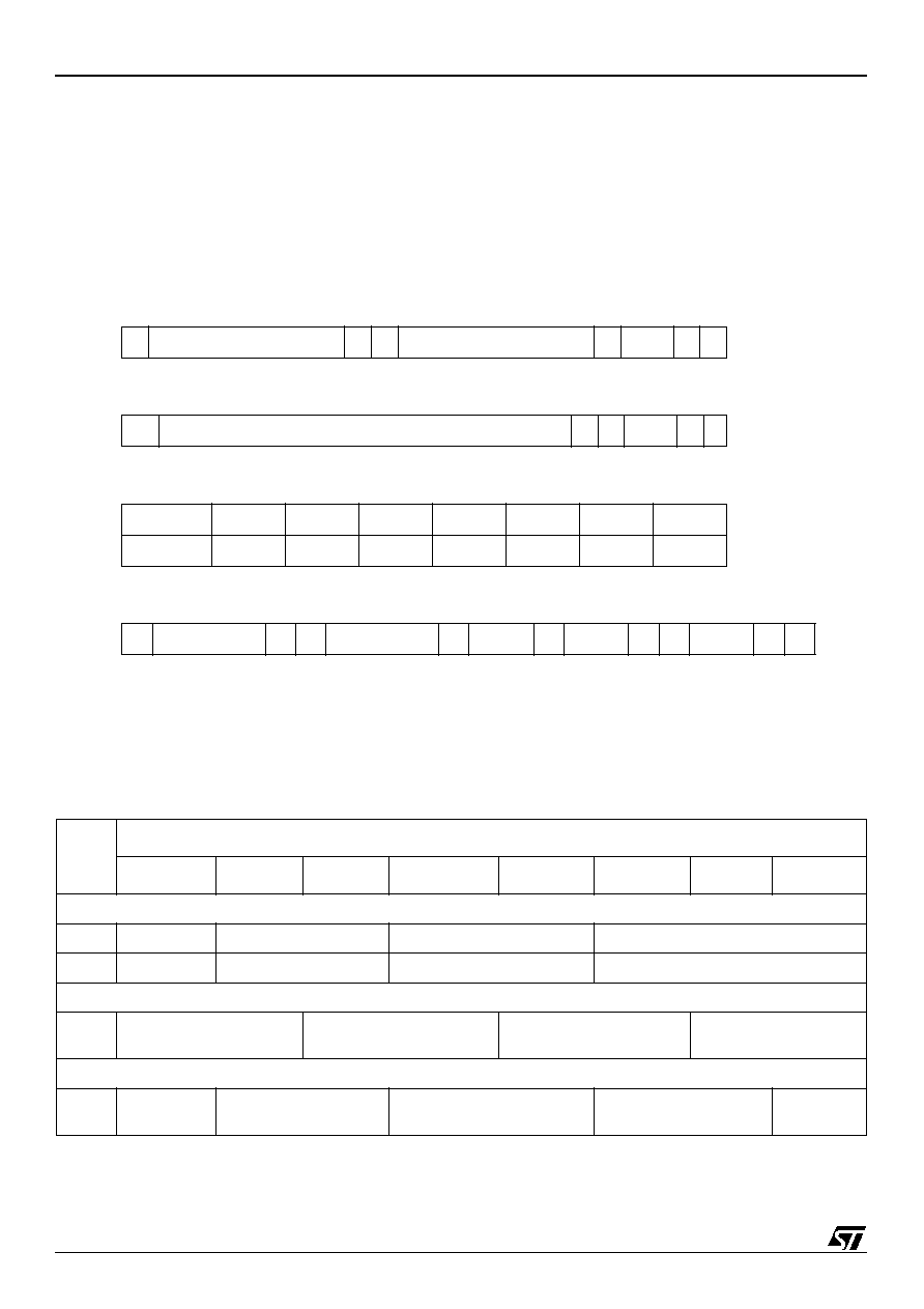
I≤C BUS SELECTION
Data transfers follow the usual I≤C format; i.e. after the start condition (S), a 7-bit slave address is
sent, followed by an eight-bit data direction bit (W). An 8-bit sub-address is sent to select a register,
followed by an 8-bit data word to be included in the register. The IC's I≤C bus decoder enables the
automatic incrementation mode in write mode.
String Format
Write only mode (S = Start condition, P = Stop condition, A = Acknowledge)
Read only mode
Slave Address
Auto Increment Mode
3.1
I≤C Bus Addresses
Write Address: 1001 0100 = 94(hex)
Input Signal Summary (Write Mode)
S
Slave Address
0
A
Sub-address
A
Data
A
P
S
Slave Address
1
A
Data
A
P
Address
A7
A6
A5
A4
A3
A2
A1
Value
1
0
0
1
0
1
0
S
Slave Address
0
A
Sub-address
A
DATA0
A
DATA1
A
....
DATAn
A
P
Sub-Address
Sub-Address +1 Sub-Address + N
Reg
Addr
(Hex)
Data
d7
d6
d5
d4
d3
d2
d1
d0
Y/CVBS and C Output Selection
00
DigOUT6
Not Used
TV Y/CVBS Output Selection
Recorder Y/CVBS Output Selection
01
DigOUT5
Not Used
Auxiliary C Output Selection
Auxiliary Y/CVBS Output Selection
RGB/YPrPb & Fast Blanking Selection
02
RGB/YPrPb
High Impedance State
RGB or YPrPb or C mode
Selection
Auxiliary or Encoder
Selection
Fast Blanking Selection
Digital Outputs
03
DIGOUT4
DIGOUT3
DIGOUT2 Control
DIGOUT1 Control
C_GATE
Control
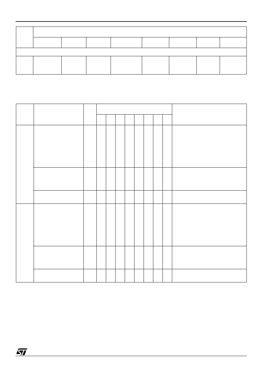
13/24
STV6618
I≤C BUS SELECTION
Note:
Unused data must be set to "0".
Standby
04
TV Output
Standby
AUX Chroma
Output
Standby
AUX CVBS
Output
Standby
REC Output
Standby
AUX Input
Disable
TV Input
Disable
TUN Input
Disable
ENC Input
Disable
Reg.
Addr
(Hex)
Description
Bits
Data
Comments
d7
d6
d5
d4
d3
d2
d1
d0
00
Recorder Y/CVBS Output
Selection
3
X
X
X
X
X
X
X
X
X
X
X
X
X
X
X
X
X
X
X
X
X
X
X
X
X
X
X
X
X
X
X
X
X
X
X
X
X
X
X
X
0
0
0
0
1
1
1
1
0
0
1
1
0
0
1
1
0
1
0
1
0
1
0
1
Mute
YIN_ENC
CVBSIN_ENC
Y/CVBSIN_AUX
Y/CVBSIN_TV
YCVBSIN_TUN
Not allowed
Not allowed
TV Y/CVBS Output
Selection
2
X
X
X
X
X
X
X
X
X
X
X
X
0
0
1
1
0
1
0
1
X
X
X
X
X
X
X
X
X
X
X
X
Y/CVBS_AUX
YIN_ENC
CVBSIN_ENC
Mute
DigOUT6 Control
1
0
1
X
X
X
X
X
X
X
X
X
X
X
X
X
X
0 = Low Level
1 = High Level
01
AUX (SCART2) Y/CVBS
Output Selection
3
X
X
X
X
X
X
X
X
X
X
X
X
X
X
X
X
X
X
X
X
X
X
X
X
X
X
X
X
X
X
X
X
X
X
X
X
X
X
X
X
0
0
0
0
1
1
1
1
0
0
1
1
0
0
1
1
0
1
0
1
0
1
0
1
Y/CVBSin_TV
YIN_ENC
CVBSIN_ENC
YCVBSIN_TUN
Mute
Not allowed
Not allowed
Not allowed
AUX (SCART2) Chroma
Output Selection
2
X
X
X
X
X
X
X
X
X
X
X
X
0
0
1
1
0
1
0
1
X
X
X
X
X
X
X
X
X
X
X
X
Mute
CIN_ENC
CIN_TV
CIN_TUN
DigOUT5 Control
1
0
1
X
X
X
X
X
X
X
X
X
X
X
X
X
X
0 = Low Level
1 = High Level
Reg
Addr
(Hex)
Data
d7
d6
d5
d4
d3
d2
d1
d0
I≤C BUS SELECTION
STV6618
14/24
Reg.
Addr
(Hex)
Description
Bits
Data
Comments
d7
d6
d5
d4
d3
d2
d1
d0
02
Fast Blanking Output Control
2
X
X
X
X
X
X
X
X
X
X
X
X
X
X
X
X
X
X
X
X
X
X
X
X
0
0
1
1
0
1
0
1
FBIN_AUX
FB forced to Low Level
FB forced to High Level
Not allowed
RGB/YPrPb Output Selection
2
X
X
X
X
X
X
X
X
X
X
X
X
X
X
X
X
0
0
1
1
0
1
0
1
X
X
X
X
X
X
X
X
RGB/YPrPb_AUX
RGB/YPrPb_ENC
CIN_ENC (pin 6) at R/Pr/COUT_TV,
B/PbOUT & G/YOUT muted
RGB/YPrPb mute
RGB or YPrPb or C Selection
2
X
X
X
X
X
X
X
X
X
X
X
X
X
X
X
X
0
0
0
0
1
1
1
1
0
0
1
1
0
0
1
1
0
0
0
0
0
0
0
0
0
1
0
1
0
1
0
1
X
X
X
X
X
X
X
X
X
X
X
X
X
X
X
X
RGB mode selection, bottom clamp at
RGB inputs, AUX. input selected
RGB mode selection, bottom clamp at
RGB inputs, ENC. input selected
CIN_AUX (pin 17)selected, average
clamp at R/Pr/CIN_AUX input,
GIN_AUX (bottom clamp) selected,
BIN_AUX (bottom clamp) selected
CIN_ENC (pin 9)selected, average
clamp at R/Pr/CIN_ENC input,
GIN_ENC (bottom clamp) selected,
BIN_ENC (bottom clamp) selected
YPrPb mode selection, sync pulse
clamp at Pr Pb inputs, black clamp at Y
input, AUX. input selected
YPrPb mode selection, sync pulse
clamp at Pr Pb inputs, black clamp at Y
input, ENC. input selected
YPrPb mode selection, delayed sync
pulse clamp at Pr Pb inputs, black
clamp at Y input, AUX. input select
YPrPb mode selection, delayed sync
pulse clamp at Pr Pb inputs, black
clamp at Y input, ENC. input select
RGB/YPrPb Control
2
0
0
1
0
1
X
X
X
X
X
X
X
X
X
X
X
X
X
X
X
X
X
X
X
RGB/YPrPb outputs active
RGB/YPrPb outputs high imp state
Red output active, Green and Blue
high imp. state
15/24
STV6618
I≤C BUS SELECTION
3.2
Power-on Reset: Bus Register Initial Conditions
Power-on Reset is active when supply V
DD
< 3.5 V. Non-significant bits (X) are pre-set to "0".
Reg.
Addr
(Hex)
Description
Bits
Data
Comments
d7
d6
d5
d4
d3
d2
d1
d0
03
C_Gate Output Control
1
X
X
X
X
X
X
X
X
X
X
X
X
X
X
0
1
Low Level
High Level
DIGOUT1
2
X
X
X
X
X
X
X
X
X
X
X
X
X
X
X
0
1
1
X
0
1
X
X
X
Low Level
Mid Level
High Level
DIGOUT2
2
X
X
X
X
X
X
X
X
X
0
1
1
X
0
1
X
X
X
X
X
X
X
X
X
Low Level
Mid Level
High Level
DIGOUT3
2
X
X
X
0
1
1
X
0
1
X
X
X
X
X
X
X
X
X
X
X
X
X
X
X
Low Level
Mid Level
High Level
DIGOUT4 Control
1
0
1
X
X
X
X
X
X
X
X
X
X
X
X
X
X
0 = Low Level
1 = High Level
04
ENC Inputs
1
X
X
X
X
X
X
X
X
X
X
X
X
X
X
0
1
Inputs Active
Inputs Disabled
TUN Inputs
1
X
X
X
X
X
X
X
X
X
X
X
X
0
1
X
X
Inputs Active
Inputs Disabled
TV Inputs
1
X
X
X
X
X
X
X
X
X
X
0
1
X
X
X
X
Inputs Active
Inputs Disabled
AUX Inputs
1
X
X
X
X
X
X
X
X
0
1
X
X
X
X
X
X
Inputs Active
Inputs Disabled
REC Outputs
1
X
X
X
X
X
X
0
1
X
X
X
X
X
X
X
X
Y/CVBSOUT_REC Outputs ON
Y/CVBSOUT_REC Outputs OFF
AUX Outputs
1
X
X
X
X
0
1
X
X
X
X
X
X
X
X
X
X
Y/CVBSOUT_AUX Outputs ON
Y/CVBSOUT_AUX Outputs OFF
COUT_AUX Output
1
X
X
0
1
X
X
X
X
X
X
X
X
X
X
X
X
COUT_AUX Outputs ON
COUT_AUX Outputs OFF (high imped.)
TV Outputs
1
0
1
X
X
X
X
X
X
X
X
X
X
X
X
X
X
TV Video Outputs ON
TV Video Outputs OFF
Full Stop
8
1
1
1
1
1
1
1
1
Only I≤C bus supplied, and digital outputs
Reg.
Addr
(Hex)
Data
Comments
d7
d6
d5
d4
d3
d2
d1
d0
00
0
0
0
0
0
0
0
0
Rec. CVBS output muted, TV CVBS output to Aux. CVBS input, Digital output
low level
01
0
0
0
0
0
0
0
0
Aux. CVBS output to TV CVBS input, Aux. Chroma output muted, Digital
output low level
02
0
0
0
0
0
0
0
0
FB output to Aux. FB input, TV RGB output to Aux. RGB inputs, RGB outputs
active
03
0
0
0
0
0
0
0
0
C_gate output low level, DIGOUT outputs low level
04
0
0
0
0
0
0
0
0
All inputs outputs active
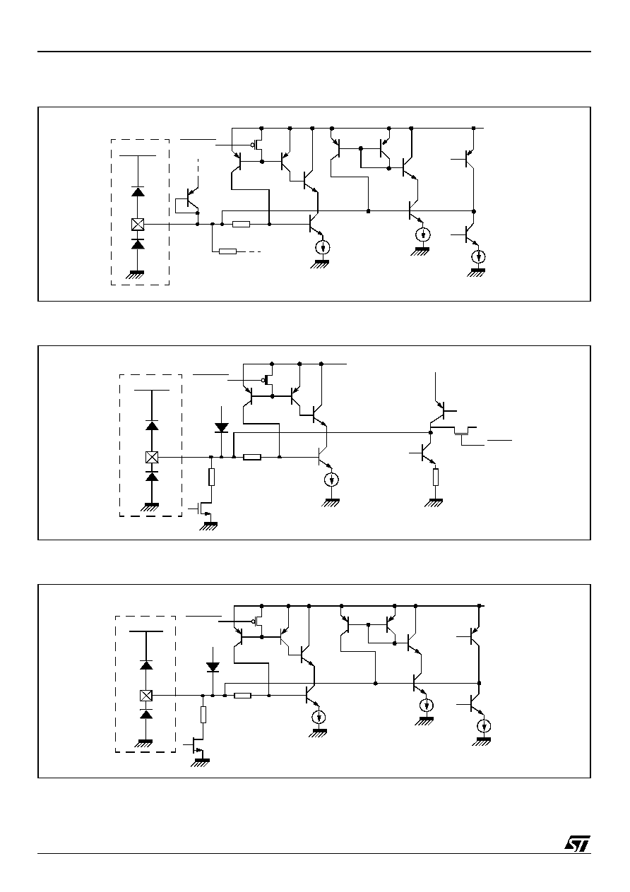
INPUT/OUTPUT GROUPS
STV6618
16/24
4
INPUT/OUTPUT GROUPS
Figure 5: C_Gate Logic Output (Pin 28)
Figure 6: Video Outputs (Pins 23, 25, 27, 29, 31 and 33)
Figure 7: YCVBSOUT_REC Recorder Output (Pin 21)
V
DD
5 V
18 k
50
V
DD
5 V
Protected Pad
V
CCB1,2,3
Protected Pad
ib
V
CCB1,2,3
V
CCB1,2,3
V
CCB_REC
5 V
Protected Pad
V
CCB_REC
5 V
Figure 8: Fast Blanking Inputs (Pin 35)
Figure 9: I≤C Bus SCL I/O (Pin 37)
Figure 10: Fast Blanking Output (Pin 34)
V
CCB3
Protected Pad
V
DD
5 V
tri
VDD_FLOAT
10 k
V
DD
5 V
Protected Pad
V
DD
V
CCB3
V
CCB3
Protected Pad
17/24
STV6618 INPUT/OUTPUT
GROUPS
Figure 11: Bottom Clamped Video Inputs
(Pins 1, 4, 7, 19 and 41)
Figure 12: DIGOUT 1, 2 and 3 (Pins 42, 44 and 2)
Figure 13: DIGOUT 4, 5 and 6 (Pins 14, 16 and 18)
15 k
V
CC
5 V
tri
V
CC
5 V
Protected Pad
5 k
2V + V
BE
Float_Bus
V
DD
5 V
Float_DigOUT
V
DD
5 V
Figure 14: Average Clamped Video Inputs
(Pins 6, 40 and 43)
Figure 15: DECV (Pin 5)
Figure 16: I≤C Bus SDA I/O (Pin 38)
25 k
V
CC
5 V
V
CC
5 V
Protected Pad
5 k
25 k
tri
Protected Pad
V
CC
5 V
Protected Pad
10 k
40 k
V
CC
5 V
V
CC
5 V
VDD_FLOAT
Acknowledge
10 k
V
DD
5 V
Protected Pad
INPUT/OUTPUT GROUPS
STV6618
18/24
Figure 17: R/Pr/C Inputs (Pins 9 and 17)
Figure 18: G/Y Inputs (Pins 10 and 15)
Figure 19: B/Pb Inputs (Pins 11 and 13)
V
CC
5 V
Protected Pad
50 k
5 k
V
CC
5 V
Botclamp
V
CC
5 V
Protected Pad
5 k
V
CC
5 V
Botclamp
15 k
2V + V
BE
20 k
sepsel
tri
V
CC
5 V
Protected Pad
5 k
V
CC
5 V
Botclamp
15 k
tri
2V + V
BE
19/24
STV6618 INPUT/OUTPUT
GROUPS
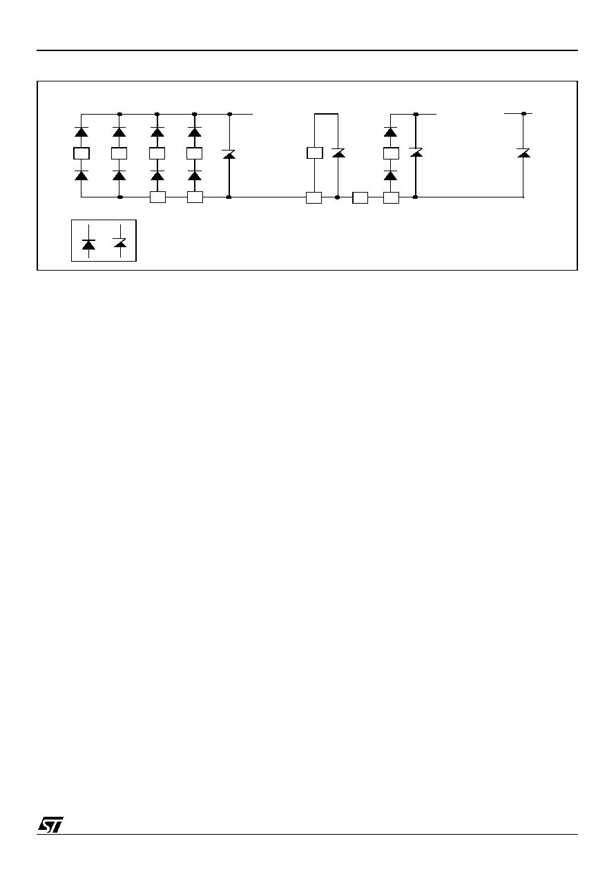
Figure 20: Power Supply Connection
These symbols represent some huge diode and Zener-like components used for ESD
protection of the device.
They are not supposed to be paths for any current in normal operation mode.
VCCB3
VCCB2
VCCB1 VCCB_REC
32
30
24
20
5 V
Float_VidOUTs
3
8
GND1
12
GND2
39
GNDD
36
V
DD
V
CC
5 V
5 V
Float_V
DD
12 V
Float_DigOUTs
26
GNDB
22
GNDB_REC
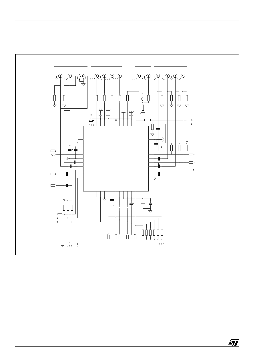
APPLICATION DIAGRAMS
STV6618
20/24
5
APPLICATION DIAGRAMS
Figure 21: YPrPb Application
R55
R40
75
J5
Y
J6
Pb
R46
10K
R41
75
AUX INPUTS
S-VHS
Y
.
.
C
R56
12V
VCC
R53
C46
100n
C41
100n
T2
NPN
C44
100n
J12
Pb
R30 to R35: expected loads
on Decoder outputs
R35
75
J3
Y/CVBS
C25
100n
R32
75
R34
75
J2
C
Tuner Y/CVBS
J11
Y
J9
Y/CVBS
ENC Y
R47
10K
R50
10K
ENC Pr
C48
100n
C29
100n
C30
100n
R49
10K
C28
10µ
R36
75
ENC Pb
DOut 2
J7
Y/CVBS
C32
100n
C42
10µ
C39
100n
R43 75
C36
1µ
ENC CVBS
C26
100n
R54
R39
75
R51
J8
C
C43
100n
SCL
DOut 6
VDD
J10
Pr
VCC
REC Y/CVBS
VCCB
C40
47n
Tuner C
J1
Y/CVBS
R37
75
ENC C
J4
Pr
DOut 4
C35
100n
R44
75
DOut 1
AUX OUTPUTS
VCCB
C33
100n
ENC Y
TV OUTPUTS
R30
75
R48
10K
C37
100n
C27
100n
VCCB
R33
75
C34
100n
R38
75
R45
10K
SDA
C38
100n
REC C
TV INPUTS
R31
75
R42
470
C31
10µ
DOut 5
DOut 3
C47
1µ
All grounds must be linked un der the IC
R52
C45
100n
U3
STV6618
4
8
6
7
5
9
10
11
3
41
40
12
19
14
17
16
15
18
13
20
21
22
25
24
23
30
33
31
32
29
28
27
34
35
36
37
38
39
42
1
44
43
2
26
CVBSI
N_
ENC
VCC
CI
N8
ENC
YI
N8
ENC
DECV
R
/
P
r
/C
IN
_
E
N
C
G
/
YI
N_
ENC
B/
Pb
I
N
_
E
NC
GND1
Y/CVBSIN_TV
CIN_TV
GND2
Y/CVBSIN_AUX
DigOUT4
R/Pr/CIN_AUX
DigOUT5
G/YIN_AUX
DigOUT6
B/PbIN_AUX
VCCB_REC
Y/CVBSOUT_REC
GNDB_REC
Y/
CVBSO
UT_
A
UX
VCCB1
COUT
_
A
UX
VCCB2
Y/
CVBSO
UT_
T
V
R
/
Pr
/
C
O
U
T_TV
VCCB3
G/
Y
O
UT
_
T
V
C_
GAT
E
B
/
P
b_O
U
T
_TV
FBOUT_TV
FBIN_AUX
VDD
SCL
SDA
GNDD
DigOUT1
Y/
CVBSI
N_
TUN
DigOUT2
CIN_TUN
Di
g
O
UT
3
GNDB
21/24
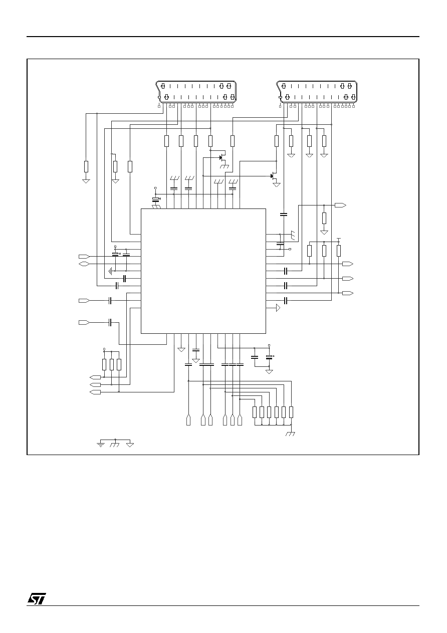
STV6618 APPLICATION
DIAGRAMS
Figure 22: 2 SCART / RGB Signal Application
ENC C
C24
100n
R8
75
C14
100n
Tuner C
R1
75
R10
75
R6
75
R28
C17
100n
DOut 1
C1
100n
R25
VCC
ENC B
DOut 4
R11
75
DOut 5
C4
10µ
R19
10K
VCCB
ENC R
All grounds must be linked un der the IC
VCC
C22
100n
C12
100n
C13
100n
C23
100n
R23
10K
R9
75
C18
10µ
R24
R4
75
C3
100n
SDA
R22
10K
R2
75
Q2
JFET N
AUX1
SCART
2
3
4
5
6
7
8
9
10
11
12
13
14
15
16
17
18
19
20
21
1
R13 to R18: expected loads
on Decoder outputs
SCL
VDD
C11
100n
C15
100n
C20
100n
R17
4K7
REC Y/CVBS
U1
STV6618
4
8
6
7
5
9
10
11
3
41
40
12
19
14
17
16
15
18
13
20
21
22
25
24
23
30
33
31
32
29
28
27
34
35
36
37
38
39
42
1
44
43
2
26
CVBSI
N_ENC
VCC
CI
N8ENC
YI
N8ENC
DECV
R/
Pr
/
C
I
N
_ENC
G/
YI
N_ENC
B/
PbI
N
_ENC
GND1
Y/CVBSIN_TV
CIN_TV
GND2
Y/CVBSIN_AUX
DigOUT4
R/Pr/CIN_AUX
DigOUT5
G/YIN_AUX
DigOUT6
B/PbIN_AUX
VCCB_REC
Y/CVBSOUT_REC
GNDB_REC
Y/
CVBSOUT_AUX
VCCB1
COUT_AUX
VCCB2
Y/
CVBSOUT_TV
R/
Pr
/
C
OUT_TV
VCCB3
G/
YOUT_TV
C_GATE
B/
Pb_OUT_TV
FBOUT_TV
FBIN_AUX
VDD
SCL
SDA
GNDD
DigOUT1
Y/
CVBSI
N_TUN
DigOUT2
CIN_TUN
Di
gOUT3
GNDB
C5
100n
R27
DOut 6
R3
75
R21
10K
C16
47n
C10
100n
12V
R20
10K
DOut 3
Tuner Y/CVBS
DOut 2
R26
C2
100n
C21
100n
C9
100n
C7
10µ
VCCB
R12
75
R29
ENC Y
TV1
SCART
2
3
4
5
6
7
8
9
10
11
12
13
14
15
16
17
18
19
20
21
1
R5
75
ENC G
C19
100n
R7
75
Q1
JFET N
ENC CVBS
C8
100n
R18
10K
C6
100n
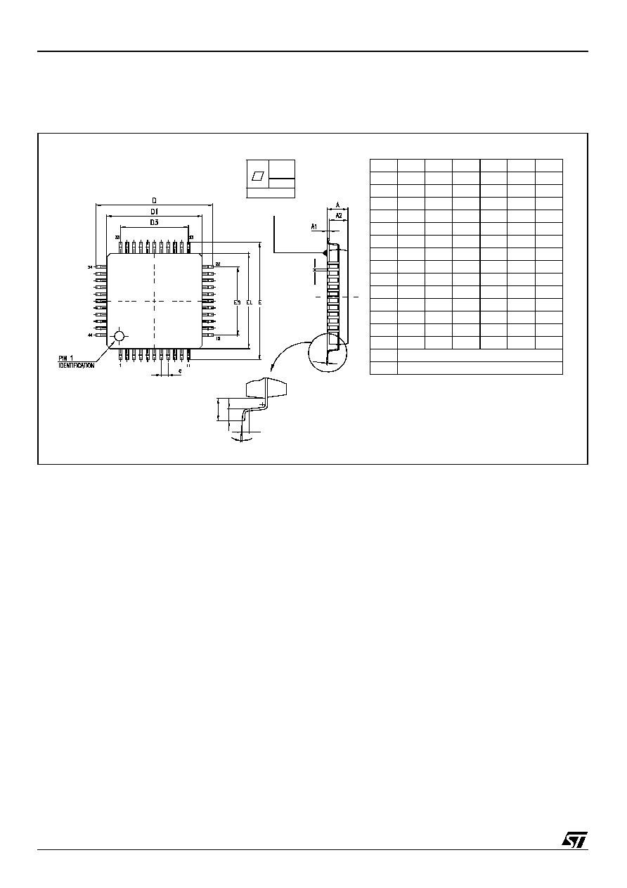
PACKAGE MECHANICAL DATA
STV6618
22/24
6
PACKAGE MECHANICAL DATA
Figure 23: 44-Pin Thin Quad Flat Package
A
1.60
0.063
A1
0.05
0.15
0.002
0.006
A2
1.35
1.40
1.45
0.053 0.055 0.057
b
0.30
0.37
0.45
0.012 0.015 0.018
c
0.09
0.20
0.004
0.008
D
12.00
0.472
D1
10.00
0.394
D3
8.00
0.315
E
12.00
0.472
E1
10.00
0.394
E3
8.00
0.315
e
0.80
0.031
K
0∞
3.5∞
7∞
L
0.45
0.60
0.75
0.018 0.024 0.030
L1
1.00
0.039
Number of Pins
N
44
b
c
L1
L
K
0.10m
m
.004
seating plane
23/24
STV6618 REVISION
HISTORY
7
REVISION HISTORY
The following table summarizes the modifications applied to this document.
Revision
Description
Date
1.0
First Issue
24 April 2001
New pinout proposal, to improve connection to TV SCART. Slight correction of electrical
parameters (changed value in Bold). Correction of DigOUT1-2-3 I≤C control specification
(changed value in bold)
27 April 2001
New pinout proposal, To improve connection to SCARTs. Application layout hypothesis: 1
layer PCB, IC on lower side (copper side), SCART on upper side
7 May 2001
Application diagrams added. VDCin chroma section: 3.0V instead of 2.3V previously.
VDCin , video section, PrPb: 3.0V instead of 2.3V previously
11 May 2001
Add Fast Blanking Section Electrical Characteristics. Update Application Schematic
Diagrams
7 June 2001
1.1
Addition of
Section 4: INPUT/OUTPUT GROUPS on page 16
.
21 June 2001
1.2
Document reformatted. Replaced
Figure 22: 2 SCART / RGB Signal Application
on page 21
.
6 July 2001
1.3
CIN = 1 VPP changed to "VIN = 1 VPP in CBW Parameter in
Section 2.6
. Symbols for a
PNP, NPN and current source as well as their connections added to
Figure 17
.
2 Oct 2001
1.4
Update of Crosstalk and DC Output voltage data in
Section 2.4
and
Section 2.6
.
Modification of Register 2 data in
Section 3.1
. Replaced
Figure 21
and
Figure 22
.
10 Oct 2001
1.5
Update of Crosstalk data and Output Voltage values in
Section 2.4
and
Section 2.6
.
Updated
Figure 3
and
Figure 22
.
26 Oct 2001
1.6
Chroma Output Gain (G6C) parameters updated in
Section 2.6
.
14 Jan 2002
1.7
Addition of minimum/maximum values for certain parameters in
Section 2: ELECTRICAL
CHARACTERISTICS
. Document upgraded to Datasheet status.
24 May 2002
1.8
Modification of Bandwidth parameter (17 MHz) and
Figure 3
.
24 Sept. 2002

REVISION HISTORY
STV6618
24/24
Information furnished is believed to be accurate and reliable. However, STMicroelectronics assumes no responsibility for the
consequences of use of such information nor for any infringement of patents or other rights of third parties which may result from its
use. No license is granted by implication or otherwise under any patent or patent rights of STMicroelectronics. Specifications
mentioned in this publication are subject to change without notice. This publication supersedes and replaces all information previously
supplied. STMicroelectronics products are not authorized for use as critical components in life support devices or systems without
express written approval of STMicroelectronics.
The ST logo is a registered trademark of STMicroelectronics
© 2003 STMicroelectronics - All Rights Reserved
STMicroelectronics GROUP OF COMPANIES
Australia - Brazil - Canada - China - Finland - France - Germany - Hong Kong - India - Israel - Italy - Japan
Malaysia - Malta - Morocco - Singapore - Spain - Sweden - Switzerland - United Kingdom - U.S.A.
www.st.com